XC7A100T-2CSG324C vs XC7A100T-L2CSG324E Comparaison
Comparaison détaillée côte à côte de XC7A100T-2CSG324C par AMD et XC7A100T-L2CSG324E par AMD. Comparez les spécifications clés, les paramètres électriques, le conditionnement, le statut de cycle de vie, les prix et la disponibilité pour déterminer le meilleur composant pour vos exigences de conception.
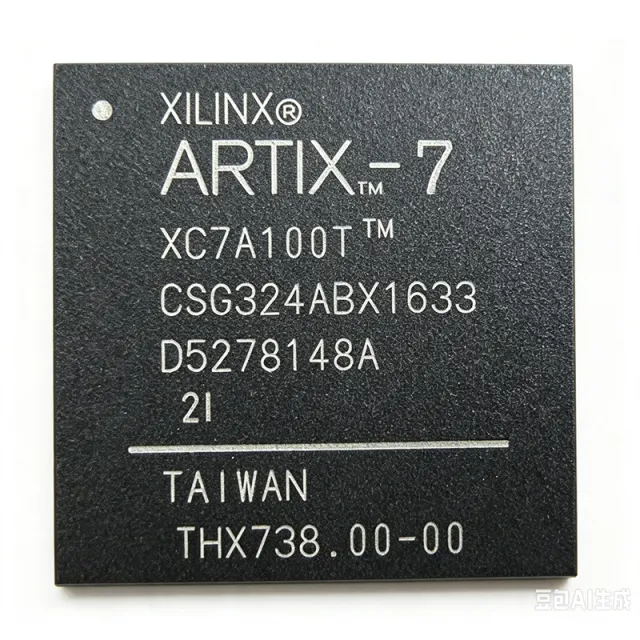

Comparaison des spécifications
| Paramètre | XC7A100T-2CSG324C | XC7A100T-L2CSG324E |
|---|---|---|
| Marque | AMD | AMD |
| Catégorie | FPGA & CPLD | FPGA & CPLD |
| Statut du cycle de vie | Actif | Actif |
| Prix unitaire (USD) | $59,50 | — |
| Family | Artix-7 | — |
| Logic Cells | 101440 | 101,440 cells |
| Block RAM | 4860 Kb | 4,860 Kb |
| DSP Slices | 240 | 240 slices |
| User I/O | 210 | — |
| Boîtier | CSBGA-324 (CSG324) | 324-terminal FC-BGA (CSG324) |
| Speed Grade | -2 | -L2 |
| Core Voltage | 1.0 V | — |
| I/O Voltage | 1.2V to 3.3V | — |
| Température de fonctionnement | 0C to +85C | — |
| Clock Management Tiles | 6 | — |
| PCIe Blocks | 1 (Gen2 x1) | — |
| Gigabit Transceivers | 4 (up to 6.6 Gbps) | — |
| Configuration | SRAM-based, supports SPI, BPI, JTAG | — |
| Statut RoHS | Compliant | — |
| FPGA Family | — | Artix-7 |
| Process Technology | — | 28 nm |
| Operating Voltage Class | — | 1 V |
| Terminal Count | — | 324 terminals |
| Temperature Grade | — | Extended, E grade |
| Junction Temperature Range | — | 0°C to 100°C |
| Type de montage | — | Surface mount |
| Programmable Logic Type | — | FPGA |
| On-Chip RAM | — | 4,860 Kb block RAM |
| Digital Signal Processing | — | 240 DSP slices |
| Configuration Memory | — | [DATA_NEEDED: configuration memory type and capacity] |
| Maximum I/O Count | — | [DATA_NEEDED: maximum user I/O count] |
| RoHS Compliance | — | [DATA_NEEDED: RoHS compliance status] |