XC7A100T-3CSG324E vs XC7A100T-2CSG324C Comparaison
Comparaison détaillée côte à côte de XC7A100T-3CSG324E par AMD et XC7A100T-2CSG324C par AMD. Comparez les spécifications clés, les paramètres électriques, le conditionnement, le statut de cycle de vie, les prix et la disponibilité pour déterminer le meilleur composant pour vos exigences de conception.

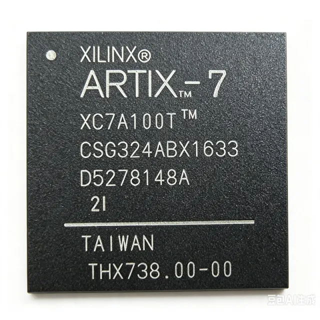
Comparaison des spécifications
| Paramètre | XC7A100T-3CSG324E | XC7A100T-2CSG324C |
|---|---|---|
| Marque | AMD | AMD |
| Catégorie | FPGA & CPLD | FPGA & CPLD |
| Statut du cycle de vie | Actif | Actif |
| Prix unitaire (USD) | — | $59,50 |
| Device Type | Artix-7 FPGA | — |
| Logic Cells | 101,440 cells | 101440 |
| Maximum Operating Frequency | 628 MHz | — |
| Input/Output Count | 210 I/O | — |
| Core Voltage Range | 950 mV to 1.05 V | — |
| Boîtier | 324-ball CSPBGA | CSBGA-324 (CSG324) |
| Package Designation | CSG324 | — |
| Type de montage | Surface mount | — |
| Speed Grade | -3 | -2 |
| Temperature Grade | Extended temperature | — |
| Clock Management | MMCM and PLL | — |
| DSP Capability | Dedicated DSP processing resources | — |
| Transceiver Capability | Integrated high-speed serial transceiver resources | — |
| Block RAM | [DATA_NEEDED: block RAM quantity] | 4860 Kb |
| Maximum Transceiver Line Rate | [DATA_NEEDED: maximum transceiver line rate] | — |
| Plage de température de fonctionnement | [DATA_NEEDED: minimum and maximum operating temperature] | — |
| Statut RoHS | [DATA_NEEDED: RoHS compliance status] | Compliant |
| REACH Status | [DATA_NEEDED: REACH compliance status] | — |
| AEC-Q100 Qualification | [DATA_NEEDED: AEC-Q100 qualification status] | — |
| Family | — | Artix-7 |
| DSP Slices | — | 240 |
| User I/O | — | 210 |
| Core Voltage | — | 1.0 V |
| I/O Voltage | — | 1.2V to 3.3V |
| Température de fonctionnement | — | 0C to +85C |
| Clock Management Tiles | — | 6 |
| PCIe Blocks | — | 1 (Gen2 x1) |
| Gigabit Transceivers | — | 4 (up to 6.6 Gbps) |
| Configuration | — | SRAM-based, supports SPI, BPI, JTAG |