XC7A100T-L2FGG484E vs XC7A100T-2FGG484I Comparaison
Comparaison détaillée côte à côte de XC7A100T-L2FGG484E par AMD et XC7A100T-2FGG484I par AMD. Comparez les spécifications clés, les paramètres électriques, le conditionnement, le statut de cycle de vie, les prix et la disponibilité pour déterminer le meilleur composant pour vos exigences de conception.

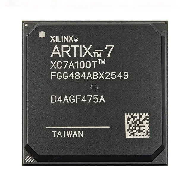
Comparaison des spécifications
| Paramètre | XC7A100T-L2FGG484E | XC7A100T-2FGG484I |
|---|---|---|
| Marque | AMD | AMD |
| Catégorie | FPGA & CPLD | FPGA & CPLD |
| Statut du cycle de vie | Actif | Actif |
| Prix unitaire (USD) | — | $45,94 |
| Device Type | Artix-7 Field-Programmable Gate Array (FPGA) | — |
| Logic Cells | 101,440 cells | 101440 |
| Configurable Logic Blocks | 7,925 CLBs | — |
| Maximum Operating Frequency | 1,286 MHz | — |
| Input/Output Count | 285 I/O | — |
| Process Technology | 28 nm CMOS | 28 nm |
| Core Supply Voltage | 1 V | 0.95 V to 1.05 V (nominal 1.0 V) |
| Boîtier | 484-pin FBGA | 484-ball FBGA (FGG484) |
| Package Designation | FGG484 | — |
| Device Family | Artix-7 | — |
| Product Series | XC7A100T | — |
| Architecture | 7-series FPGA | — |
| Programming Technology | Configuration memory | — |
| Type de montage | Surface mount | Surface Mount |
| Packaging Form | Tray | — |
| Statut RoHS | [DATA_NEEDED: RoHS status] | — |
| REACH Status | [DATA_NEEDED: REACH status] | — |
| AEC-Q100 Qualification | [DATA_NEEDED: AEC-Q100 qualification] | — |
| Plage de température de fonctionnement | [DATA_NEEDED: operating temperature range] | — |
| User I/O | — | 285 |
| Block RAM | — | 4976640 bits |
| DSP Slices | — | 240 (DSP48E1) |
| Clock Management Tiles | — | 10 (MMCM + PLL) |
| Speed Grade | — | -2 |
| Maximum Fabric Frequency | — | 628 MHz |
| Package Dimensions | — | 23 mm x 23 mm |
| Température de fonctionnement | — | -40C to +100C (Industrial) |
| Memory Interface | — | DDR3 up to 1066 Mb/s |
| Soft Processor Support | — | MicroBlaze |
| Analog Mixed Signal | — | XADC 12-bit ADC (on-chip voltage and temperature monitoring) |