XCKU5P-2FFVB676I vs XCKU5P-L2FFVB676E Comparaison
Comparaison détaillée côte à côte de XCKU5P-2FFVB676I par AMD et XCKU5P-L2FFVB676E par AMD. Comparez les spécifications clés, les paramètres électriques, le conditionnement, le statut de cycle de vie, les prix et la disponibilité pour déterminer le meilleur composant pour vos exigences de conception.
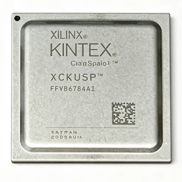

Comparaison des spécifications
| Paramètre | XCKU5P-2FFVB676I | XCKU5P-L2FFVB676E |
|---|---|---|
| Marque | AMD | AMD |
| Catégorie | FPGA & CPLD | FPGA & CPLD |
| Statut du cycle de vie | Actif | Actif |
| Prix unitaire (USD) | $1 660,00 | — |
| Family | Kintex UltraScale+ | — |
| Logic Cells | 474600 | — |
| System Logic Cells | 474600 | — |
| Block RAM | 41984000 bits | — |
| User I/O | 280 | — |
| Maximum Internal Clock Frequency | 725 MHz | — |
| Core Supply Voltage | 825 mV to 876 mV | 0.698 V to 0.876 V |
| Speed Grade | -2 | L2, -2 speed grade |
| Clock Management | MMCM, PLL | — |
| Process Technology | 16 nm FinFET | — |
| Boîtier | 676-BBGA, FCBGA (FFVB676) | 676-pin FCBGA |
| Terminal Form | Ball | — |
| Type de montage | Surface Mount | [DATA_NEEDED: surface-mount mounting classification] |
| Température de fonctionnement | -40C to +100C (Industrial) | — |
| Temperature Grading | Industrial (I) | — |
| Statut RoHS | Compliant | — |
| Device Type | — | Kintex UltraScale+ FPGA |
| Logic Blocks | — | 216,960 blocks |
| Macrocells | — | 474,600 macrocells |
| LAB or CLB Count | — | 27,120 LABs/CLBs |
| Total RAM Bits | — | 41,984,000 bits |
| Equivalent RAM Capacity | — | 16,900 Kbit |
| User I/O Count | — | 280 pins |
| Nominal Core Voltage | — | 0.72 V |
| Junction Temperature Range | — | 0 °C to 110 °C |
| Logic Type | — | Field-programmable gate array |
| Device Family | — | Kintex UltraScale+ |
| DSP Compute Performance | — | 6.3 TeraMACs for the device family |
| Backplane Transceiver Classes | — | 16G and 28G for the device family |
| RoHS Compliance | — | Compliant |
| REACH Compliance | — | Compliant |
| DRC Conflict Status | — | Conflict Free |
| Programmable Flash Capacity | — | [DATA_NEEDED: configuration flash capacity] |
| Transceiver Count | — | [DATA_NEEDED: exact transceiver count] |
| DSP Block Count | — | [DATA_NEEDED: exact DSP block count] |