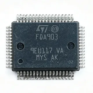
FDA803Q - 1A, 35V Ultra-Low Noise LDO | Texas Instruments
Référence : FDA803Q ✓ Actif| Qté | Prix unitaire | Total |
|---|---|---|
| 1 | $4.85 | $4,85 |
| 10 | $4.36 | $43,60 |
| 100 | $3.88 | $388,00 |
| 500 | $3.49 | $1 745,00 |
| 1 000 | $3.1 | $3 100,00 |
FDA803Q Présentation
An LDO (Low-Dropout) linear regulator is a type of voltage regulator that maintains a stable output voltage even when the input voltage is very close to the output voltage. It operates by dissipating excess power as heat, providing a clean, low-noise output. LDOs are essential in power management ICs, serving as the final stage in a power supply chain to filter out ripple and noise from switching regulators. The FDA803Q fits into the hierarchy: LDO -> linear regulator -> voltage regulator -> power management IC -> semiconductor.
Key features include 4.17 uVrms output noise (20 Hz to 100 kHz), 72 dB PSRR at 1 kHz, and a low dropout voltage of 200 mV at full 1A load. The device also offers 6.4 mA quiescent current, an active-high enable pin for power sequencing, and thermal shutdown protection. The VQFN-20 package provides a thermal resistance of 31.4 C/W, enabling compact designs without external heatsinking at moderate power levels.
The FDA803Q utilizes a bipolar architecture with a precision bandgap reference, achieving noise performance comparable to discrete reference designs while maintaining regulator simplicity. The high PSRR minimizes ripple from upstream switching converters, making it suitable for noise-sensitive analog and RF signal chains where clean power rails are critical.
Typical applications include high-end audio DAC power supplies, PLL/VCO power rails in RF transceivers, precision ADC/DAC reference buffering, and test and measurement instrumentation. The wide input range also supports industrial 24V bus systems with adequate headroom.
When designing with this device, ensure adequate input-to-output voltage headroom to maintain regulation under all load conditions. The enable pin allows sequential power-up in multi-rail systems, which is essential for processors requiring specific rail sequencing.
Alternatives de remplacement direct pour FDA803Q — même boîtier, compatible broche à broche. Les références à boîtier différent nécessitant une retouche du PCB sont exclues.
Variantes de cette série
Modèles de la même série directement compatibles avec FDA803Q (même facteur de forme et même empreinte) — différant par Enable Pin, Input Voltage Range, MSL Level, Output Type, Output Voltage Range.
Outil de comparaison rapide — sélectionnez des références alternatives pour une comparaison côte à côte :
TPS7A4700RGWR
✅ Remplacement direct✓ En stock
$3.6591 / unité
Voir la fiche technique →TPS7A4701RGWR-Q1
✅ Remplacement direct📋 Alternative de référence (hors catalogue)
TPS7A4701RGWT
✅ Remplacement direct📋 Alternative de référence (hors catalogue)
LT3045EDC
✅ Remplacement direct ⚠️ Spécifications non vérifiées📋 Alternative de référence (hors catalogue)
ADM7150ARDZ
✅ Remplacement direct ⚠️ Spécifications non vérifiées📋 Alternative de référence (hors catalogue)
FDA803Q Valeurs maximales et caractéristiques électriques
| Type de sortie | Adjustable |
| Plage de tension de sortie | 1.4 V to 34 V |
| Courant de sortie maximal | 1 A |
| Plage de tension d'entrée | 3 V to 35 V |
| Tension de déchet | 200 mV at 1 A |
| Bruit de sortie | 4.17 uVrms (20 Hz to 100 kHz) |
| PSRR | 72 dB at 1 kHz |
| Courant de repos | 6.4 mA |
| Résistance thermique | 31.4 C/W |
| Température de fonctionnement | -40C to +125C |
| Boîtier | VQFN-20 (RGW) 5x5 mm |
| Type de montage | Surface Mount |
| Niveau MSL | 2 (1 year) |
| Statut RoHS | Compliant |
| Broche d'activation | Yes (active-high) |
Configuration des broches de FDA803Q
| Broche 1 | OUT — Regulated output voltage |
| Broche 5 | GND — Ground |
| Broche 6 | EN — Enable (active high) |
| Broche 7 | IN — Input supply |
| Broche 9 | NR/SS — Noise reduction/soft-start capacitor |
| Broche 10 | FB — Feedback for output voltage setting |
| Broche 13 | GND — Ground |
| Broche 17 | OUT — Regulated output voltage |
| Broche 20 | IN — Input supply |
| Broche 21 | PAD — Exposed thermal pad (connect to GND) |
Applications typiques
FDA803Q convient pour 6 applications: High-End Audio DAC Power Supply, RF Transceiver Power Supply, Precision ADC Reference Buffer, Industrial 24V Bus Power, Test and Measurement Instrumentation, Portable Medical Devices.
High-End Audio DAC Power Supply
Provides clean 5V rail for audio DACs with 4.17uVrms noise. The FDA803Q's ultra-low noise and high PSRR ensure that the power supply does not introduce audible artifacts into the audio signal. In a typical audio DAC application, the FDA803Q is placed between the system 5V rail and the DAC's AVDD pin, with a 10uF ceramic capacitor on input and output. Compared to switching regulators, the LDO eliminates switching noise but dissipates more power; for a 12V-to-5V conversion at 500mA, power dissipation is 3.5W, requiring adequate thermal management.
Recommandé
RF Transceiver Power Supply
Powers PLL/VCO circuits with 72dB PSRR at 1kHz, minimizing phase noise. The FDA803Q's high PSRR suppresses ripple from upstream switching regulators, which is critical for RF signal integrity. In an RF transceiver, the FDA803Q is used to power the VCO and PLL, with a 0.1uF capacitor close to the VCC pin to filter high-frequency noise. The low noise floor of 4.17uVrms ensures that the power supply does not contribute to phase noise, improving overall system performance.
Recommandé
Precision ADC Reference Buffer
Buffers reference voltage for 24-bit ADCs with 4.17uVrms noise. The FDA803Q's low noise and high accuracy make it ideal for driving the reference input of precision ADCs. In a data acquisition system, the FDA803Q is used to generate a clean 5V reference from a noisy 12V rail, with a 10uF capacitor on the output to stabilize the reference. The low dropout voltage of 200mV ensures that the reference remains regulated even with input voltage variations.
Recommandé
Industrial 24V Bus Power
Regulates 24V industrial bus to 5V for sensors and microcontrollers. The FDA803Q's wide input range of up to 35V makes it suitable for industrial applications where the supply voltage can vary. In a factory automation system, the FDA803Q is used to power a microcontroller and sensors from a 24V bus, with a 10uF input capacitor to handle transients. The thermal shutdown protection ensures safe operation in harsh environments.
Recommandé
Test and Measurement Instrumentation
Provides clean power for oscilloscopes and signal generators. The FDA803Q's low noise and high PSRR are essential for maintaining measurement accuracy. In a benchtop instrument, the FDA803Q is used to power analog front-end circuits, with a 10uF output capacitor to reduce noise. The enable pin allows for power sequencing in multi-rail systems, ensuring that sensitive analog circuits power up after digital circuits.
Recommandé
Portable Medical Devices
Powers low-noise analog front-ends in portable monitors. The FDA803Q's low quiescent current of 6.4mA extends battery life in portable devices. In a portable ECG monitor, the FDA803Q is used to power the analog front-end, with a 10uF output capacitor to filter noise. The small VQFN-20 package saves board space, and the wide input range accommodates battery voltage variations.
Recommandé
Récapitulatif des produits recommandés
Données de référence d'ingénierie pour FDA803Q — comparaison, recommandations de conception et informations de conformité.
Guide de sélection
Comparaison avec les alternatives
| Paramètre | Ce produit | TPS7A4700RGWR | TPS7A4701RGWR-Q1 | TPS7A3301RGWR |
|---|---|---|---|---|
| Package | VQFN-20 (RGW) | VQFN-20 (RGW) - same | VQFN-20 (RGW) - same | VQFN-20 (RGW) - same |
| Brand | Texas Instruments | Texas Instruments | Texas Instruments | Texas Instruments |
| Output Current | 1 A | 1 A | 1 A | 1 A (negative) |
| Output Voltage Range | 1.4V to 34V | 1.4V to 34V | 1.4V to 34V | -36V to -1.4V |
| Enable Pin | Yes (active-high) | No | Yes (active-high) | Yes (active-high) |
| Automotive Grade | No | No | Yes (AEC-Q100) | No |
| Output Noise | 4.17 uVrms | 4.17 uVrms | 4.17 uVrms | 3.8 uVrms |
| PSRR at 1kHz | 72 dB | 72 dB | 72 dB | 75 dB |
Principaux différenciateurs
- Only VQFN-20 family member with enable pin (vs TPS7A4700RGWR)
- Automotive grade option available (vs TPS7A4701RGWR-Q1)
- Positive voltage polarity (vs TPS7A3301RGWR)
Notes de conception
At VIN=12V, VOUT=5V, and 1A load, power dissipation is 7W. The VQFN-20 package has theta_JA of 31.4 C/W, resulting in a 220C junction temperature rise. A heatsink or at least 1 square inch of copper pour is required for reliable operation above 2W dissipation.
Place input and output capacitors as close to the IC pins as possible. Use a 10uF ceramic capacitor on the input and a 10uF ceramic capacitor on the output. Add a 0.1uF ceramic capacitor in parallel for high-frequency noise bypass.
Do not exceed the maximum input voltage of 35V. Ensure the external resistor divider uses 1% or better tolerance resistors to maintain output voltage accuracy. The NR/SS capacitor controls startup time and noise bandwidth - do not omit it.
Informations de conformité
RoHS compliant per TI product page. Not AEC-Q100 qualified - choose TPS7A4701RGWR-Q1 for automotive.