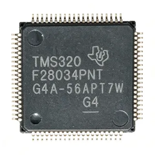
MSP430FR5994IPNR - 16MHz 256KB FRAM MCU | Texas Instruments
Référence : MSP430FR5994IPNR ✓ Actif| Qté | Prix unitaire | Total |
|---|---|---|
| 1 | $1.92 | $1,92 |
| 10 | $1.82 | $18,20 |
| 100 | $1.7 | $170,00 |
| 500 | $1.55 | $775,00 |
| 1 000 | $1.42 | $1 420,00 |
MSP430FR5994IPNR Présentation
FRAM (ferroelectric random access memory) is a nonvolatile memory technology that combines the speed and low power of SRAM-like writes with the data retention of flash. In a microcontroller system hierarchy, the MSP430FR5994 sits within the broader family of mixed-signal MCUs, occupying the memory-and-signal-processing tier of the MSP430FR599x series, which targets battery-powered and energy-harvesting applications that require both large nonvolatile memory and mathematical computation.
Key differentiating features include the LEA (Low-Energy Accelerator), a vector math coprocessor that offloads FFT, FIR, and matrix operations from the CPU while the core remains in a low-power state; hardware AES cryptography for secure data handling; a 12-bit ADC and analog comparator for sensing front ends; and direct memory access (DMA) for peripheral-to-memory transfers without CPU intervention. FRAM offers 100x faster writes than flash with inherently low write energy and virtually unlimited write endurance.
Architecturally, the MSP430 CPUXV2 16-bit RISC core is paired with multiple low-power modes, enabling active currents in the microamp-per-MHz class while retaining RAM and peripheral state. The unified FRAM memory allows flexible partitioning between code and data, and the MPU (memory protection unit) can segment FRAM into protected regions for bootloader and data-logging designs.
Typical applications include portable medical and health monitoring devices, building and factory sensor nodes, energy metering front ends, and battery-powered signal processing where the LEA accelerates FFT-based vibration or acoustic analysis.
A key design consideration is the FRAM write protection scheme: configure the MPU segments early in development to prevent accidental data corruption, and respect the maximum operating frequency versus supply voltage relationship documented in the manufacturer datasheet.
This page synthesizes distributor pricing, same-family drop-in alternatives, and practical design notes not found in the manufacturer datasheet.
Alternatives de remplacement direct pour MSP430FR5994IPNR — même boîtier, compatible broche à broche. Les références à boîtier différent nécessitant une retouche du PCB sont exclues.
Variantes de cette série
Modèles de la même série directement compatibles avec MSP430FR5994IPNR (même facteur de forme et même empreinte) — différant par DMA Channels.
Outil de comparaison rapide — sélectionnez des références alternatives pour une comparaison côte à côte :
MSP430FR59941IPNR
✅ Remplacement direct📋 Alternative de référence (hors catalogue)
MSP430FR5964IPNR
✅ Remplacement direct📋 Alternative de référence (hors catalogue)
MSP430FR5994IPNR Valeurs maximales et caractéristiques électriques
| Core Processor | MSP430 CPUXV2 |
| Core Size | 16-Bit |
| Fréquence d'horloge maximale | 16 MHz |
| Program Memory Type | FRAM |
| Program Memory Size | 256KB (256K x 8) |
| RAM Size | 8KB SRAM |
| Hardware Accelerator | LEA (Low-Energy Accelerator) |
| Security Feature | AES |
| ADC Resolution | 12-bit |
| Analog Comparator | Yes |
| DMA Channels | Yes |
| Connectivity | UART, SPI, I2C |
| Peripherals | Timer |
| Boîtier | 80-LQFP (12x12 mm) |
| Type de montage | Surface Mount |
| Plage de température de fonctionnement | -40C to +85C |
Guide de configuration des broches du MSP430FR5994IPNR 80-lqfp (12x12 mm)
Configuration des broches du MSP430FR5994IPNR (boîtier 80-lqfp (12x12 mm)). Ce circuit intégré numérique comprend des GPIO, des interfaces de communication (UART, SPI, I2C) et des broches d'alimentation. Consultez la fiche technique du fabricant pour les fonctions alternatives des broches et les options de configuration. Indispensable pour la conception de systèmes embarqués et la conception de circuits imprimés.

Aucune donnée de brochage détaillée disponible pour MSP430FR5994IPNR.
Consultez la fiche technique pour la configuration complète des broches.
Applications typiques
MSP430FR5994IPNR convient pour 6 applications: Portable Health Monitoring, Industrial Condition Monitoring, Building and Factory Sensor Nodes, Energy Metering, Battery-Powered Data Loggers, Audio and Acoustic Sensing.
Portable Health Monitoring
The MSP430FR5994IPNR fits wearable and portable medical devices because its 16-bit ultra-low-power MSP430 core minimizes battery drain during continuous biosignal acquisition, and its 12-bit ADC digitizes ECG, PPG, or bioimpedance front ends directly. The LEA accelerator performs real-time filtering and feature extraction while the CPU sleeps, and the 256KB FRAM logs patient data with fast, low-energy writes that extend coin-cell life. Placed as the main MCU between an analog front end and a BLE or sub-GHz radio, it processes and buffers samples in the 8KB SRAM before transmission. The trade-off versus higher-performance MCUs is the 16 MHz ceiling, sufficient for biosignal rates but not for heavy imaging workloads.
Recommandé
Industrial Condition Monitoring
For vibration and acoustic condition monitoring of motors and rotating machinery, the MSP430FR5994IPNR samples accelerometer data through its 12-bit ADC and uses the LEA accelerator to compute FFTs locally, detecting bearing or imbalance signatures without streaming raw data to a gateway. The 256KB FRAM buffers measurement history across power cycles, surviving write-heavy logging thanks to FRAM endurance. Running from a battery or energy harvester, the MCU spends most time in low-power modes and wakes on timer or ADC thresholds. Designers should budget SRAM carefully, since FFT window buffers consume a large share of the 8KB SRAM; reducing window length or bit depth trades frequency resolution for memory headroom.
Recommandé
Building and Factory Sensor Nodes
Wireless sensor nodes for smart buildings benefit from the MSP430FR5994IPNR's combination of ultra-low-power standby, UART/SPI/I2C connectivity to radios and sensors, and AES hardware encryption for secure network joins and data privacy. The 256KB FRAM supports over-the-air update staging and configuration storage without external memory, and DMA moves sensor data while the CPU remains asleep. A typical node connects environmental sensors via I2C and a sub-GHz or 2.4 GHz radio via SPI, waking on a timer to sample, encrypt, and transmit. The 16 MHz core is ample for protocol stacks; the main design constraint is peripheral count versus pin budget on the 80-pin LQFP.
Recommandé
Energy Metering
Electricity and submetering products use the MSP430FR5994IPNR's 12-bit ADC or an external metrology ADC to sample voltage and current channels, then apply the LEA accelerator to compute RMS, power factor, and harmonic content with low energy per sample. FRAM stores billing and tamper logs that must survive power interruptions and millions of write cycles, a task where flash-based MCUs degrade. Hardware AES secures metering data and firmware images in accordance with utility security requirements. The MCU interfaces to the metrology front end over SPI and to a display or communication module over UART. Designers must observe the datasheet supply-voltage-to-frequency curve to run reliably across the industrial -40C to +85C range.
Recommandé
Battery-Powered Data Loggers
Standalone data loggers are a natural fit for the MSP430FR5994IPNR because FRAM eliminates the erase-before-write penalty of flash, enabling high-frequency logging with minimal energy per record. The MPU can partition the 256KB FRAM into a protected firmware segment and an append-only data segment, protecting logged data across code updates and brownouts as discussed in TI E2E design threads. Sensors attach over I2C or SPI, DMA streams readings into FRAM, and a real-time timer wakes the system from low-power modes at programmable intervals. Retrieved loggers offload data over UART. The key limitation is the 8KB SRAM working buffer, which bounds burst-sampling rates before data must be committed to FRAM.
Recommandé
Audio and Acoustic Sensing
Low-power acoustic applications such as glass-break detectors, leak detectors, and keyword spotting use the MSP430FR5994IPNR with a MEMS microphone feeding the 12-bit ADC, while the LEA accelerator executes FIR filters and FFTs in hardware offload. TI positions LEA explicitly for digital signal processing workloads, and DSPLib routines map directly onto it, keeping energy per transform low enough for always-on listening from battery power. The 256KB FRAM stores feature models and event buffers for later radio transmission. Developers should use 16-bit fixed-point math aligned to LEA vector widths and partition SRAM so the input window, filter state, and LEA working areas do not collide within the 8KB budget.
Recommandé
Récapitulatif des produits recommandés
Données de référence d'ingénierie pour MSP430FR5994IPNR — comparaison, recommandations de conception et informations de conformité.
Guide de sélection
Comparaison avec les alternatives
| Paramètre | Ce produit | MSP430FR59941IPNR | MSP430FR5964IPNR |
|---|---|---|---|
| Package | 80-LQFP (12x12 mm) | 80-LQFP (12x12 mm) - same | 80-LQFP (12x12 mm) - same |
| Brand | Texas Instruments | Texas Instruments | Texas Instruments |
| Core / Frequency | MSP430 CPUXV2, 16-Bit, 16 MHz | MSP430 CPUXV2, 16-Bit, 16 MHz | MSP430 CPUXV2, 16-Bit, 16 MHz |
| Program Memory | 256KB FRAM | 256KB FRAM | 256KB FRAM |
| SRAM | 8KB | 8KB | 8KB |
| LEA Accelerator | Yes | Yes | No |
| Operating Temperature | -40C to +85C | -40C to +85C | -40C to +85C |
Principaux différenciateurs
- Integrated LEA vector math accelerator (vs MSP430FR5964IPNR)
- 256KB unified FRAM with MPU segmentation (vs MSP430FR59941IPNR)
- Hardware AES security (vs MSP430FR5964IPNR)
Notes de conception
Estimate the energy budget by counting FRAM writes: FRAM write energy is far lower than flash, but the distinction matters for coin-cell designs logging continuously. Keep the CPU in the deepest applicable LPM mode between ADC samples and use DMA to move conversion results into FRAM or SRAM without waking the core. Always consult the manufacturer datasheet for exact per-mode current figures before finalizing battery sizing, as the active current and standby figures for this device are not reproduced in this page's verified data.
Configure the MPU (Memory Protection Unit) FRAM segmentation early in the project, as raised in TI E2E design discussions: without MPU segments, firmware bugs or re-flashed code can overwrite persistent data stored in FRAM. Reserve the lowest segment for code, and protect the data-log segment as read-only for the application. Also respect the maximum operating frequency versus supply voltage relationship in the datasheet when running from low-battery rails, since undervoltage at 16 MHz causes marginal execution.
Place 100 nF ceramic decoupling capacitors at each VCC/VSS pin pair of the 80-LQFP as close to the package as possible, plus one bulk 4.7 uF to 10 uF capacitor near the supply entry. The 12x12 mm LQFP has a center thermal relief area on the land pattern; tie unused exposed pads to ground per the datasheet land-pattern drawing. Keep the analog ADC input traces short and away from the crystal and radio SPI lines to minimize crosstalk into sensing channels.
For LEA-accelerated sampling, buffer alignment matters: the LEA requires properly aligned data blocks (per TI's DSPLib documentation) in SRAM, so declare FFT input/output arrays with the required alignment pragmas and verify with the LEA runtime checks enabled during development. Misaligned buffers cause silent errors or fault conditions that are difficult to trace in production firmware.
Informations de conformité
Compliance status was not stated in the provided verified data. Confirm RoHS/REACH status on the TI product page quality section before specifying.