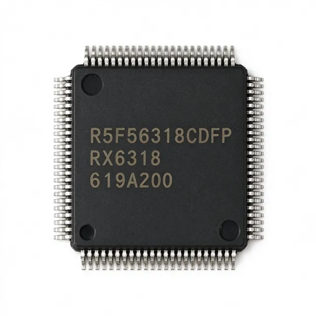
R5F56318CDFP#V0 - RX631 100MHz 512KB Flash MCU | Renesas
Référence : R5F56318CDFP#V0 ✓ Actif| Qté | Prix unitaire | Total |
|---|---|---|
| 1 | $27.5625 | $27,56 |
| 10 | $19.9063 | $199,06 |
| 100 | $17.6094 | $1 760,94 |
| 500 | $16.8438 | $8 421,90 |
| 1 000 | $16.0781 | $16 078,10 |
R5F56318CDFP#V0 Présentation
A microcontroller (MCU) is a single-chip computer that integrates a CPU, memory, and programmable peripherals on a single silicon die. MCUs are the heart of embedded systems, ranging from home appliances and industrial controllers to automotive ECUs and IoT edge nodes. The RX family sits in the high-performance 32-bit MCU tier alongside ARM Cortex-M, RISC-V, and proprietary cores, offering deterministic real-time behavior and rich connectivity. Within that hierarchy, the RX631 is an Ethernet-less variant of the RX63N, traded off to enable lower-cost designs that still require the full peripheral set.
The R5F56318CDFP#V0 integrates a 12-bit ADC with up to 21 channels, motor-control timers, multiple SCI (UART), RSPI, I2C, and CAN interfaces. It supports 2.5V and 3.3V operation and incorporates safety and security features suitable for industrial and consumer designs. The LFQFP-100 package provides ample I/O for connectivity-rich applications while remaining manageable on a 2-layer PCB with careful layout.
Typical applications include industrial motor control, building automation controllers, factory equipment HMI panels, and consumer devices with graphical interfaces. The combination of CAN, multiple serial channels, and ADC performance also makes it suitable for sensor aggregation nodes and small inverter drives.
When designing with the R5F56318CDFP#V0, place a 4.7 uF bulk capacitor and 100 nF decoupling capacitor near each VCC pin pair. For CAN communications, add a 120 ohm termination resistor at each bus end. Avoid routing high-speed signals under the MCU to prevent coupling noise into the analog supply.
This page synthesizes distributor pricing, drop-in Renesas RX family alternatives, and practical PCB layout guidance not consolidated in the manufacturer datasheet.
Alternatives de remplacement direct pour R5F56318CDFP#V0 — même boîtier, compatible broche à broche. Les références à boîtier différent nécessitant une retouche du PCB sont exclues.
Variantes de cette série
Modèles de la même série directement compatibles avec R5F56318CDFP#V0 (même facteur de forme et même empreinte) — différant par ADC, Communication Interfaces, Core Architecture, Operating Temperature, Operating Voltage.
Outil de comparaison rapide — sélectionnez des références alternatives pour une comparaison côte à côte :
R5F56318DDFP#V0
📋 Alternative de référence (hors catalogue)
R5F56318CDFP#10
📋 Alternative de référence (hors catalogue)
R5F563N0CDFP#V0
📋 Alternative de référence (hors catalogue)
R5F56318CDFC#V0
📋 Alternative de référence (hors catalogue)
R5F563NDCDFC#V0
📋 Alternative de référence (hors catalogue)
R5F56318CDFP#V0 Valeurs maximales et caractéristiques électriques
| Core Architecture | RXv1 32-bit RISC |
| Core Frequency | 100 MHz |
| Flash Memory | 512 KB |
| SRAM | 128 KB |
| Operating Voltage | 2.5 V / 3.3 V |
| Boîtier | 100-LFQFP (14x14 mm) |
| Type de montage | Surface Mount |
| ADC | 12-bit, up to 21 channels |
| Timers | Motor-control timers, 16-bit MTU |
| Communication Interfaces | SCI, RSPI, I2C, CAN |
| Ethernet | Not present (RX631, no Ethernet controller) |
| USB | Available on selected channels |
| Température de fonctionnement | -40 C to +85 C (industrial) |
| Niveau MSL | 3 (168 hours) |
| Statut RoHS | Compliant |
| Lead-Free | Yes |
Configuration des broches de R5F56318CDFP#V0
| Broche 1 | VREFH — ADC analog reference high (3.3V) |
| Broche 2 | VREFL — ADC analog reference low (0V) |
| Broche 3 | AVCC — Analog supply voltage |
| Broche 4 | AVSS — Analog ground |
| Broche 5 | P40 — General purpose I/O |
| Broche 6 | P41 — General purpose I/O |
| Broche 7 | P42 — General purpose I/O |
| Broche 8 | P43 — General purpose I/O |
| Broche 9 | P44 — General purpose I/O |
| Broche 10 | P45 — General purpose I/O |
| Broche 11 | P46 — General purpose I/O |
| Broche 12 | P47 — General purpose I/O / IRQ |
| Broche 13 | P50 — General purpose I/O / WAIT |
| Broche 14 | P51 — General purpose I/O |
| Broche 15 | P52 — General purpose I/O |
| Broche 16 | P53 — General purpose I/O |
| Broche 17 | P54 — General purpose I/O / EDREQ |
| Broche 18 | P55 — General purpose I/O / EDACK |
| Broche 19 | P56 — General purpose I/O |
| Broche 20 | P57 — General purpose I/O |
| Broche 21 | VCC — Digital supply voltage |
| Broche 22 | VSS — Digital ground |
| Broche 23 | P10 — General purpose I/O / MTIOC0B |
| Broche 24 | P11 — General purpose I/O / MTIOC0A |
| Broche 25 | P12 — General purpose I/O / MTIOC0C |
| Broche 26 | P13 — General purpose I/O / MTIOC0D |
| Broche 27 | P14 — General purpose I/O / MTIOC1A |
| Broche 28 | P15 — General purpose I/O / MTIOC1B |
| Broche 29 | P16 — General purpose I/O / MTIOC1C |
| Broche 30 | P17 — General purpose I/O / MTIOC1D |
| Broche 31 | P20 — General purpose I/O / MTIOC2A |
| Broche 32 | P21 — General purpose I/O / MTIOC2B |
| Broche 33 | P22 — General purpose I/O / MTIOC2C |
| Broche 34 | P23 — General purpose I/O / MTIOC2D |
| Broche 35 | P24 — General purpose I/O / MTIOC3A |
| Broche 36 | P25 — General purpose I/O / MTIOC3B |
| Broche 37 | P26 — General purpose I/O / MTIOC3C |
| Broche 38 | P27 — General purpose I/O / MTIOC3D |
| Broche 39 | P30 — General purpose I/O / MTIOC4A |
| Broche 40 | P31 — General purpose I/O / MTIOC4B |
| Broche 41 | P32 — General purpose I/O / MTIOC4C |
| Broche 42 | P33 — General purpose I/O / MTIOC4D |
| Broche 43 | P34 — General purpose I/O / MTIOC6A |
| Broche 44 | P35 — General purpose I/O / MTIOC6B |
| Broche 45 | P36 — General purpose I/O / MTIOC6C |
| Broche 46 | P37 — General purpose I/O / MTIOC6D |
| Broche 47 | P60 — General purpose I/O / SS0 |
| Broche 48 | P61 — General purpose I/O / MOSI0 |
| Broche 49 | P62 — General purpose I/O / MISO0 |
| Broche 50 | P63 — General purpose I/O / RSPCK0 |
| Broche 51 | P64 — General purpose I/O / SSL0 |
| Broche 52 | P65 — General purpose I/O / MOSI1 |
| Broche 53 | P66 — General purpose I/O / MISO1 |
| Broche 54 | P67 — General purpose I/O / RSPCK1 |
| Broche 55 | P70 — General purpose I/O / RxD0 |
| Broche 56 | P71 — General purpose I/O / TxD0 |
| Broche 57 | P72 — General purpose I/O / RxD1 |
| Broche 58 | P73 — General purpose I/O / TxD1 |
| Broche 59 | P74 — General purpose I/O / SDA0 |
| Broche 60 | P75 — General purpose I/O / SCL0 |
| Broche 61 | P76 — General purpose I/O / RxD2 |
| Broche 62 | P77 — General purpose I/O / TxD2 |
| Broche 63 | P80 — General purpose I/O / CAN RX |
| Broche 64 | P81 — General purpose I/O / CAN TX |
| Broche 65 | VCC — Digital supply voltage |
| Broche 66 | VSS — Digital ground |
| Broche 67 | P82 — General purpose I/O / CAN RX2 |
| Broche 68 | P83 — General purpose I/O / CAN TX2 |
| Broche 69 | P84 — General purpose I/O / IRQ4 |
| Broche 70 | P85 — General purpose I/O / IRQ5 |
| Broche 71 | P86 — General purpose I/O / IRQ6 |
| Broche 72 | P87 — General purpose I/O / IRQ7 |
| Broche 73 | P90 — General purpose I/O / USB_DP |
| Broche 74 | P91 — General purpose I/O / USB_DM |
| Broche 75 | P92 — General purpose I/O / USB_VBUS |
| Broche 76 | P93 — General purpose I/O |
| Broche 77 | P94 — General purpose I/O / AN104 |
| Broche 78 | P95 — General purpose I/O / AN105 |
| Broche 79 | P96 — General purpose I/O / AN106 |
| Broche 80 | P97 — General purpose I/O / AN107 |
| Broche 81 | P100 — General purpose I/O / AN108 |
| Broche 82 | P101 — General purpose I/O / AN109 |
| Broche 83 | P102 — General purpose I/O / AN110 |
| Broche 84 | P103 — General purpose I/O / AN111 |
| Broche 85 | P104 — General purpose I/O / AN112 |
| Broche 86 | P105 — General purpose I/O / AN113 |
| Broche 87 | P106 — General purpose I/O / AN114 |
| Broche 88 | P107 — General purpose I/O / AN115 |
| Broche 89 | P120 — General purpose I/O / AN116 |
| Broche 90 | P121 — General purpose I/O / XIN |
| Broche 91 | P122 — General purpose I/O / XOUT |
| Broche 92 | P123 — General purpose I/O |
| Broche 93 | P124 — General purpose I/O / AN117 |
| Broche 94 | P125 — General purpose I/O / NMI |
| Broche 95 | MD — Mode-select (programming/debug) |
| Broche 96 | RES — Reset (active low) |
| Broche 97 | XTAL — Crystal oscillator connection |
| Broche 98 | EXTAL — External clock / crystal |
| Broche 99 | VCC — Digital supply voltage |
| Broche 100 | VSS — Digital ground |
Applications typiques
R5F56318CDFP#V0 convient pour 7 applications: Industrial Motor Control, Building Automation Controller, Factory Equipment HMI Panels, Sensor Aggregation Nodes, Small Inverter Drives, Consumer Connectivity Devices, Industrial Sensor / Metering.
Industrial Motor Control
The R5F56318CDFP#V0 fits industrial motor control because its 100 MHz RXv1 core executes three-phase field-oriented control (FOC) loops in real time. The on-chip motor-control timers deliver complementary PWM with dead-time insertion, and the 12-bit ADC supports simultaneous current-sense sampling on multiple channels (typical 1 us conversion). The 512 KB flash holds both the FOC algorithm and CANopen / Modbus stacks; 128 KB SRAM absorbs real-time trace buffers. Unlike a generic Cortex-M0, this part has dedicated hardware-trigger synchronization between timer and ADC, simplifying critical ISR timing. Power dissipation at 100 MHz is roughly 240 mW typical, well within the LFQFP-100 thermal envelope.
Recommandé
Building Automation Controller
For HVAC and building-automation hubs, the R5F56318CDFP#V0 provides RS-485-capable SCI channels, I2C sensor buses, and on-chip CAN for inter-zone networking without external transceivers beyond the standard isolators. Its 512 KB flash supports BACnet or Modbus application stacks plus a real-time scheduler, while 128 KB SRAM accommodates buffer pools for multiple concurrent sensor polls. The industrial temperature range of -40 C to +85 C is rated for unconditioned electrical-room installations. Compared with smaller Cortex-M0+ parts, the RX631 offers deterministic interrupt latency (<10 cycles) critical for protocol-timed responses in BACnet MS/TP.
Recommandé
Factory Equipment HMI Panels
HMI operator panels benefit from the R5F56318CDFP#V0's combination of CAN, multiple UARTs, and sufficient flash to host a small graphical library and touch UI without external memory. Designers typically pair the MCU with an SPI-driven TFT controller; RSPI supports up to 20 MHz to drive mid-size displays without DMA bottlenecks. The 100-LFQFP package exposes enough GPIO for keypad matrix, encoder inputs, and status LEDs. Industrial EMI immunity is helped by the device's separate analog/digital supply domains on the LFQFP-100 variant, allowing local filtering to limit conducted emissions on noisy factory floors.
Recommandé
Sensor Aggregation Nodes
The R5F56318CDFP#V0 suits sensor aggregation gateways that consolidate multiple analog and digital sensors onto an industry-standard bus. The 12-bit ADC (up to 21 channels) handles analog environmental sensors directly; the I2C and SCI peripherals connect to UART-based digital sensors in parallel. With 128 KB SRAM and 512 KB flash, designers can implement local filtering, threshold detection, and CAN or RS-485 uplinks. Unlike smaller MCUs, the RX631's DMA controller offloads serial data movement, freeing the 100 MHz core for application logic. Power consumption is ~240 mW typical, suitable for cabinet-mounted equipment.
Recommandé
Small Inverter Drives
For small three-phase inverter drives (typically <2 kW), the R5F56318CDFP#V0 provides the timers, ADC, and computational performance required for sensorless FOC. Its 100 MHz RXv1 core completes vector transformations inside 10 us, well inside PWM periods. Hardware dead-time insertion on the motor-control timer prevents shoot-through on the half-bridge. The wide 2.5-3.3 V analog supply tolerates noisy DC-bus conditions common in inverter designs. Designers typically add a small heatsink or copper pour for 1-2 W dissipation during sustained switching transients.
Recommandé
Consumer Connectivity Devices
Although primarily industrial-targeted, the R5F56318CDFP#V0 also finds use in higher-end consumer devices requiring CAN or multiple UART interfaces (for example, smart appliances or connected audio systems). Its 512 KB flash accommodates Wi-Fi/BLE module command stacks plus a local UI library, while SCI and I2C handle sensor and user-interface peripherals. The 100-LFQFP footprint accommodates 1.6 mm PCB pitch, easing routing on 4-layer consumer boards. Compared with Cortex-M4 alternatives, the RX core offers faster exception entry suited to time-critical motor or audio synchronization.
Recommandé
Industrial Sensor / Metering
For industrial flow meters, pressure transducers, and similar instrumentation, the R5F56318CDFP#V0 provides 12-bit ADC resolution at sufficient sample rates for process-variable filtering. The 100-LFQFP's analog-rich pinout separates AVCC and VCC, improving noise performance for measurement accuracy. Integrated CAN enables direct connection to industrial fieldbus networks without protocol converters. The -40 C to +85 C temperature grade suits outdoor metering enclosures, while 128 KB SRAM buffers time-stamped data before batch upload. Renesas' long-term product longevity program supports industrial metering design cycles.
Recommandé
Récapitulatif des produits recommandés
Données de référence d'ingénierie pour R5F56318CDFP#V0 — comparaison, recommandations de conception et informations de conformité.
Guide de sélection
Comparaison avec les alternatives
| Paramètre | Ce produit | R5F56318DDFP#V0 | R5F56318CDFP#10 | R5F563N0CDFP#V0 | R5F56318CDFC#V0 | R5F563NDCDFC#V0 |
|---|---|---|---|---|---|---|
| Brand | Renesas Electronics | Renesas Electronics | Renesas Electronics | Renesas Electronics | Renesas Electronics | Renesas Electronics |
| Package | 100-LFQFP (14x14 mm) | 100-LFQFP (14x14) - same | 100-LFQFP (14x14) - same | 100-LFQFP (14x14) - same | 100-LQFP - same | 100-LFQFP - same |
| Core | RXv1 32-bit | RXv1 32-bit | RXv1 32-bit | RXv1 32-bit | RXv1 32-bit | RXv1 32-bit |
| Core Frequency | 100 MHz | 100 MHz | 100 MHz | 100 MHz | 100 MHz | 100 MHz |
| Flash Memory | 512 KB | 512 KB | 512 KB | 512 KB | 512 KB | 512 KB |
| SRAM | 128 KB | 128 KB | 128 KB | 128 KB | 128 KB | 128 KB |
| Ethernet Controller | No (RX631, no Ethernet) | No | No | Yes (RX63N) | No | Yes (RX63N) |
| CAN Channels | 1 (CAN0) on selected pins | 1 | 1 | 1 | 1 | 1 |
| 12-bit ADC Channels | Up to 21 channels | Up to 21 | Up to 21 | Up to 21 | Up to 21 | Up to 21 |
| Operating Voltage | 2.5 V / 3.3 V | 2.5 V / 3.3 V | 2.5 V / 3.3 V | 2.5 V / 3.3 V | 2.5 V / 3.3 V | 2.5 V / 3.3 V |
Principaux différenciateurs
- Wide operating voltage range supports battery and 3.3V-only designs (vs R5F56318DDFP#V0)
- No Ethernet controller integrated - lower cost than RX63N alternatives (vs R5F563N0CDFP#V0)
- Pin-compatible with RX63N and RX631 family members (vs R5F563NDCDFC#V0)
Notes de conception
Place a 4.7 uF bulk capacitor and 100 nF ceramic capacitor within 5 mm of each VCC pin pair on the LFQFP-100 package. The MCU has multiple VCC/VSS pairs (pins 21/22, 65/66, 99/100) plus separate AVCC/AVSS for the ADC (pins 3/4); use a ferrite bead or pi-filter between digital and analog supplies for noise isolation in motor-control and metering designs where ADC measurements are sensitive.
Use a 4-layer PCB with a continuous ground plane under the MCU; route high-speed signals (RSPI, SCI clocks) on the top layer above an unbroken GND plane to control impedance. Place the crystal (XIN/XOUT, pins 91/92) within 5 mm of the MCU, surrounded by a guard trace tied to GND. Avoid routing analog and digital signals across split planes on inner layers.
Do not operate the R5F56318CDFP#V0 above 100 MHz without verifying that the FLASH_WAIT register is configured for the operating frequency. Programming with wait=0 at 100 MHz will cause unstable flash reads. The MD pin (pin 95) must be pulled HIGH through 1-10 kohm for normal boot; an external supervisor or JTAG debugger can also control this pin. Ensure the reset (RES#) line has a 10 kohm pull-up to VCC and a 1 nF delay capacitor for clean brown-out behavior.
Informations de conformité
Industrial-grade part - not AEC-Q100 qualified for automotive. Lead-free LFQFP packaging. Halogen-free status not explicitly confirmed in retrieved data.
