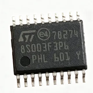
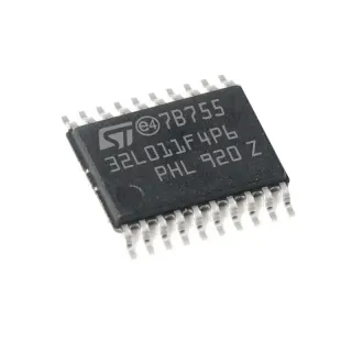
STM8S103F2P6 - 16MHz 8-Bit 4KB MCU | STMicroelectronics
Référence : STM8S103F2P6 ✓ ActifSTM8S103F2P6 Présentation
An 8-bit microcontroller is a semiconductor that executes instructions and processes sensor, control, and communications data using an 8-bit data path. The STM8S family combines a microcontroller, memory, and peripherals in one integrated circuit. Within the product hierarchy, the STM8S103F2P6 is an 8-bit MCU, an embedded controller, and a semiconductor intended for low-cost, compact electronic systems.
The principal features include a 16 MHz operating frequency, 4 KB of Flash memory, a 10-bit analog-to-digital converter, three timers, and support for UART, SPI, and I2C serial communication. The 20-TSSOP surface-mount package also supports space-constrained PCB layouts. Together, these resources allow a design to combine analog measurement, periodic timing, digital control, and peripheral communication without requiring a separate ADC or communications transceiver.
The STM8S103F2 uses the advanced STM8 core with Harvard architecture and a three-stage pipeline, as identified in the manufacturer datasheet search result. Its Harvard architecture separates instruction and data access paths, while the three-stage pipeline supports efficient sequential execution. Integrated data EEPROM is listed as a family feature by STMicroelectronics, although the exact EEPROM size for this orderable MPN is not present in the supplied verified data.
Typical applications include industrial sensor modules, compact motor and relay controllers, digital thermometers, appliance interfaces, low-cost serial bridges, LED-control boards, and compact instrumentation. The ADC supports analog input acquisition, while UART, SPI, and I2C provide paths for external sensors, displays, memory devices, and system controllers. The three timers support periodic events, timing bases, and basic control functions.
A key design consideration is verifying the exact pin multiplexing and peripheral assignments for the selected 20-TSSOP footprint in the manufacturer pinout and datasheet. Designers should also confirm memory requirements, clock configuration, ADC accuracy needs, and communication-voltage levels before committing the part to a new PCB. A complete 20-pin pinout was not included in the supplied verified excerpts and is therefore not reproduced here.
This page combines verified distributor identification, manufacturer feature information, package details, application guidance, and honest cross-reference analysis. It also distinguishes verified drop-in candidates from functional alternatives so procurement and engineering teams can evaluate interchangeability without relying on incomplete distributor metadata.
Alternatives de remplacement direct pour STM8S103F2P6 — même boîtier, compatible broche à broche. Les références à boîtier différent nécessitant une retouche du PCB sont exclues.
Variantes de cette série
Modèles de la même série directement compatibles avec STM8S103F2P6 (même facteur de forme et même empreinte) — différant par Flash Program Memory, ADC Resolution, Integrated Data EEPROM, Microcontroller Type, Package Width.
STM8S103F3P3
✅ Remplacement direct ⚠️ Spécifications non vérifiéesContactez-nous pour le prix
Voir la fiche technique →STM8S103F3P6TR
✅ Remplacement direct📋 Alternative de référence (hors catalogue)
STM8S103F2P6 Valeurs maximales et caractéristiques électriques
| Product Type | 8-bit microcontroller (MCU) |
| Product Series | STM8S103 access line |
| Fréquence d'horloge maximale | 16 MHz |
| Flash Program Memory | 4 KB (4K x 8) |
| ADC Resolution | 10 bit |
| Timer Count | 3 timers |
| Serial Interfaces | UART, SPI, and I2C |
| Core Architecture | STM8 core with Harvard architecture and 3-stage pipeline |
| Boîtier | 20-TSSOP |
| Package Dimensions | 4.40 mm width |
| Type de montage | Surface mount |
Guide de configuration des broches du STM8S103F2P6 4.40 mm width
Configuration des broches du STM8S103F2P6 (boîtier 4.40 mm width). Ce circuit intégré numérique comprend des GPIO, des interfaces de communication (UART, SPI, I2C) et des broches d'alimentation. Consultez la fiche technique du fabricant pour les fonctions alternatives des broches et les options de configuration. Indispensable pour la conception de systèmes embarqués et la conception de circuits imprimés.

Aucune donnée de brochage détaillée disponible pour STM8S103F2P6.
Consultez la fiche technique pour la configuration complète des broches.
Applications typiques
STM8S103F2P6 convient pour 6 applications: Industrial Sensor Node, Digital Thermometer, Compact Motor Controller, Appliance Control Board, LED Illumination Controller, Low-Cost Serial Bridge.
Industrial Sensor Node
STM8S103F2P6 fits a compact industrial sensor node because it combines a 10-bit ADC with a 16 MHz STM8 core and three timers in a 20-TSSOP package. The ADC can acquire analog sensor signals, while the timers support periodic sampling and control events. UART, SPI, or I2C can connect the node to a local sensor, display, or gateway. The 4 KB Flash limit should be checked against firmware, calibration tables, and update requirements before deployment.
Digital Thermometer
The STM8S103F2P6 can serve as the controller in a digital thermometer by sampling a resistive or semiconductor sensor with its 10-bit ADC. Its 16 MHz processing rate supports responsive conversion, filtering, display refresh, and button handling, while UART provides a convenient path for calibrated temperature data. The 20-TSSOP package helps reduce board area. The 4 KB program-memory budget is sufficient for compact code, although the exact ADC accuracy and calibration behavior must be evaluated from the full datasheet.
Compact Motor Controller
STM8S103F2P6 is appropriate for a small motor-control module that uses timed outputs, position or speed sensing, and a simple serial command interface. Its three timers provide resources for periodic control tasks, the ADC can monitor an analog feedback signal, and UART or SPI can connect to an external driver or supervisory controller. The 4 KB firmware limit constrains complex algorithms, so timing, protection logic, and motor-profile storage must be scoped carefully for the available flash.
Appliance Control Board
The STM8S103F2P6 fits cost-sensitive appliance controls that coordinate buttons, relays, indicators, and serial sensors. Its 16 MHz core supports responsive state-machine control, while the three timers can organize debounce, periodic scanning, and output timing. UART, SPI, and I2C offer flexible connections to displays, EEPROM, or external modules. In a mains-adjacent product, the MCU logic must remain separated from hazardous circuitry and supplemented by the required isolation and protection.
LED Illumination Controller
STM8S103F2P6 can control addressable or multi-channel LED lighting by generating precise timing with its three timers and exchanging configuration data through UART, SPI, or I2C. The 16 MHz core is suitable for animation, status effects, and user-interface logic, while the ADC supports potentiometer or ambient-light control when configured for the application. Board sizing should include driver transistors, current-limiting or constant-current circuitry, thermal management, and decoupling for the external LED power stage.
Low-Cost Serial Bridge
STM8S103F2P6 can implement a compact protocol-conversion or sensor-hub board because it provides UART, SPI, and I2C in one 8-bit device. The 16 MHz core can translate frames, validate data, and manage status indicators, while integrated EEPROM support provides a place for configuration data. The 20-TSSOP package limits board size, and the 4 KB Flash budget favors compact firmware. Protocol timing, bus levels, and input filtering must be checked during hardware design.
Données de référence d'ingénierie pour STM8S103F2P6 — comparaison, recommandations de conception et informations de conformité.
Guide de sélection
Comparaison avec les alternatives
| Paramètre | Ce produit | STM8S103F3P3 | STM8S103F3P6TR |
|---|---|---|---|
| Package | 20-TSSOP | 20-TSSOP | 20-TSSOP |
| Brand | STMicroelectronics | STMicroelectronics | STMicroelectronics |
| Maximum Clock Frequency | 16 MHz | 16 MHz | 16 MHz |
| Flash Program Memory | 4 KB | 8 KB | 8 KB |
| Architecture | 8-bit MCU | 8-bit MCU | 8-bit MCU |
| ADC Resolution | 10 bit | 10 bit | 10 bit |
| Timer Count | 3 timers | 3 timers | 3 timers |
| Serial Interfaces | UART, SPI, and I2C | UART, SPI, and I2C | UART, SPI, and I2C |
Principaux différenciateurs
- Lower verified Flash capacity for cost-sensitive firmware (vs STM8S103F3P3)
- Same 16 MHz access-line performance (vs STM8S103F3P6TR)
- Non-reel orderable designation (vs STM8S103F3P6TR)
Notes de conception
Place the MCU's decoupling capacitor adjacent to its supply pins, keep the 20-TSSOP footprint within the manufacturer's land-pattern guidance, and reserve the programming or debug signals for straightforward in-circuit programming. Because the supplied excerpts do not include the complete pin map, verify power, ground, reset, and programming pins against the official datasheet before routing. This is particularly important for the F3 alternatives, whose 8 KB Flash changes firmware layout even though the package remains 20-TSSOP.
Do not treat the STM8S003F3P6 and STM8S103K3T6 models named by a distributor as automatic replacements merely because they have similar cores and peripherals. The supplied data does not establish their exact package and pin compatibility with the STM8S103F2P6. Compare every package pin, alternate function, ADC channel, timer channel, clock pin, reset behavior, and electrical limit before approving either part as a drop-in substitution.
Keep the MCU supply and analog-input design consistent with the official electrical limits, which are not included in the supplied excerpts. Provide local bypass at the device and separate noisy digital switching from sensitive analog routing. When the ADC measures a sensor, minimize ground potential differences and account for the analog input's full-scale range; these checks are required because the verified data confirms a 10-bit ADC but does not provide its input voltage, reference, accuracy, or acquisition-time specifications.
Reserve UART, SPI, and I2C routing for the exact pins enabled by the package and device configuration. SPI can be sensitive to clock-edge timing and return-path continuity, while I2C benefits from clean routing and appropriate bus capacitance. Although the STM8S103F2P6 integrates these interfaces, pin multiplexing differs across orderable family members. Confirm the pin table and alternate-function mapping for the exact suffix rather than carrying a layout forward from an STM8S003 or STM8S103K3 design.
Informations de conformité
The supplied verified excerpts do not explicitly state this orderable part's compliance status. AEC-Q100 status is unknown because no qualification statement was provided. A search result mentions RoHS and REACH comparison topics but does not provide a verified declaration for STM8S103F2P6.