מוצרים (46,000+)

XC7K420T-L2FFG901E - 416,960-LC Kintex-7 FPGA | AMD
XC7K420T-L2FFG901E

XC7K420T-L2FFG901E - 416,960-LC Kintex-7 FPGA | AMD

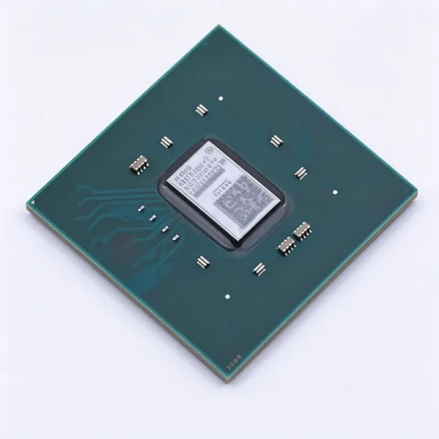
The AMD XC7K420T-L2FFG901E is a Kintex-7 field-programmable gate array with 416,960 logic cells, 32,575 configurable logic blocks, and 380 user I/O in a 901-ball FCBGA package. Built on 28 nm CMOS technology, this device is designed for high-performance parallel processing, networking, industrial control, test equipment, and high-speed signal-processing systems. The -2L speed designation identifies the lower-power Kintex-7 grade, which is screened for lower maximum static power and can operate at lower core voltages than the standard -2 grade. A field-programmable gate array is a semiconductor whose digital logic, interfaces, and signal-processing resources are configured after manufacture. Within the product hierarchy, an FPGA is a programmable-logic device, while the Kintex-7 family sits between general-purpose Artix-7 devices and higher-performance Virtex devices. This positioning makes the XC7K420T appropriate when a design requires substantial parallel logic, high-speed I/O, DSP processing, and deterministic accelerator-style performance without moving to the largest Virtex devices. The Kintex-7 family supports 28 nm programmable logic and high-speed connectivity such as PCIe Gen3 and 10 Gigabit Ethernet through suitable transceivers and soft or hard IP. Its large logic fabric allows designers to parallelize data movement, implement protocol engines, accelerate convolutional and finite-field operations, and combine multiple processing pipelines in one device. The 901-ball FCBGA provides dense I/O access for designs using many memory, clock, serial, and parallel interfaces. The -2L grade is screened for lower maximum static power and may use lower core voltages than the standard -2 grade. This distinction is important for systems constrained by thermal design, power density, or energy-per-operation targets. Exact clocking, I/O-standard, and power specifications must be selected from the device, package, speed-grade, and temperature-grade tables in the AMD Kintex-7 data sheet. Typical applications include 10 Gigabit Ethernet packet processing, PCIe Gen3 endpoint or root-port designs, industrial machine vision, radar and signal processing, test-and-measurement instrumentation, high-speed storage controllers, and communications equipment. Because the device supports many serial and parallel interfaces, PCB design must pay close attention to power delivery, ball-grid escape routing, differential-pair integrity, and thermal dissipation. For a new design, use the AMD Kintex-7 package pinout files and UG475 when assigning every ball and reviewing I/O standards. Place decoupling capacitors close to the device, control power sequencing according to the data sheet, and validate high-speed channels with appropriate simulation and measurement. Device configuration, clocking, and bitstream generation require AMD Vivado support for the selected XC7K420T variant. This page combines the verified device identity, package characteristics, speed-grade context, pinout resources, sourcing guidance, drop-in variants, and engineering guidance needed to evaluate the XC7K420T-L2FFG901E for a new programmable-logic platform.

RFQ צור קשר
XC7K420T-L2FFV901E - 416,960-Cell Kintex-7 FPGA | AMD
XC7K420T-L2FFV901E

XC7K420T-L2FFV901E - 416,960-Cell Kintex-7 FPGA | AMD

The AMD XC7K420T-L2FFV901E is a Kintex-7 field-programmable gate array with 416,960 logic cells, 380 user I/O, and 30,060 Kb of block RAM, supplied in a 900-ball FCBGA package. Built on 28 nm CMOS technology, the device combines programmable logic, DSP48E processing resources, block RAM, high-speed serial transceivers, and general-purpose I/O in a single monolithic device. The L2 speed grade targets lower static power than the standard -2 grade and is screened to operate at reduced core voltages for lower dynamic power. A field-programmable gate array, or FPGA, is a programmable digital integrated circuit whose logic, interconnect, and I/O behavior are configured after manufacture. FPGAs occupy the upper tier of the semiconductor hierarchy above standard cells and below application-specific integrated circuits, providing a practical balance between performance, design flexibility, and unit cost. The Kintex-7 family is positioned between lower-cost Artix-7 devices and higher-end Virtex devices. The XC7K420T-L2FFV901E provides 32,575 configurable logic blocks according to the product listing and offers 30,060 Kb of block RAM for buffering, packet storage, and general data processing. Its 380 I/O support board-level connectivity, while the programmable logic and DSP resources allow parallel algorithms, control paths, and signal processing to be consolidated into one device. Supported high-speed connectivity includes mainstream standards such as PCIe Gen3 and 10 Gigabit Ethernet. The L2 designation is important in power-sensitive deployments because AMD describes -2L devices as being screened for lower maximum static power and as capable of operating at lower core voltages than -2 devices. This characteristic can reduce thermal load when the design does not require the highest performance grade, although final power depends on utilization, clocking, I/O activity, and the selected I/O standards. Typical applications include high-throughput data acquisition, industrial control and test equipment, network acceleration, radar and signal processing, high-performance computing nodes, and communications infrastructure requiring multiple high-speed transceivers. The large logic and RAM inventory also suits FPGA-based prototyping of advanced algorithms without requiring a custom ASIC. PCB design must treat the 900-ball FCBGA as a high-density, thermally sensitive assembly. Follow the AMD Kintex-7 package pinout files and device datasheet for ball assignments, power-plane segmentation, decoupling, and via-in-pad requirements. Validate the selected speed grade against timing constraints rather than relying on nominal device-family specifications. This page consolidates the exact part identity, package details, resource counts, drop-in family options, comparison parameters, and practical implementation guidance for engineers evaluating the XC7K420T-L2FFV901E in high-density FPGA designs.

RFQ צור קשר
XC7K480T-1FFG901I - Kintex-7 FPGA 477K Logic Cells | AMD
XC7K480T-1FFG901I

XC7K480T-1FFG901I - Kintex-7 FPGA 477K Logic Cells | AMD

The AMD XC7K480T-1FFG901I is a high-performance Kintex-7 Field Programmable Gate Array (FPGA) from the Kintex-7 family, offering 477,760 logic cells and 35,205,120 block RAM bits in a 900-ball FCBGA package. It provides 380 user I/O pins and operates over an industrial temperature range of -40°C to +100°C. This device is designed for high-bandwidth, high-capacity applications requiring significant logic density and DSP resources. A Field Programmable Gate Array (FPGA) is an integrated circuit that can be configured by the customer or designer after manufacturing. FPGAs are part of the programmable logic device family, sitting between ASICs and CPLDs in complexity. They contain a matrix of configurable logic blocks (CLBs) connected via programmable interconnects, allowing for highly parallel, custom digital logic implementations. FPGAs are used in a wide range of applications from telecommunications and aerospace to automotive and data centers. The XC7K480T-1FFG901I features the Kintex-7 architecture, which balances performance, power, and cost. It includes 1,920 DSP slices for high-speed digital signal processing, 380 user I/Os supporting various I/O standards, and 35.2 Mb of block RAM. The -1 speed grade offers a balanced performance point, while the industrial temperature grade (-I) ensures reliable operation in harsh environments. The device supports configuration through multiple methods including JTAG, master/slave SPI, and SelectMAP. This FPGA is built on a 28nm process technology, providing a good balance of power efficiency and logic density. The 900-ball FCBGA package (FFG901) offers excellent thermal and electrical characteristics for high-performance designs. With 477,760 logic cells, it can implement complex systems-on-chip, including soft-core processors, high-speed serial transceivers, and sophisticated DSP algorithms. Typical applications include high-performance computing, wired and wireless communications, aerospace and defense systems, medical imaging, and broadcast video processing. The device's high logic density and DSP capabilities make it suitable for implementing complex algorithms in hardware. When designing with this FPGA, careful attention must be paid to power supply decoupling, clock management, and thermal management to ensure reliable operation at full capacity.

RFQ צור קשר
XC7K480T-2FFG1156I - Kintex-7 FPGA 477K Logic Cells | AMD
XC7K480T-2FFG1156I

XC7K480T-2FFG1156I - Kintex-7 FPGA 477K Logic Cells | AMD

The AMD XC7K480T-2FFG1156I is a high-performance Kintex-7 Field Programmable Gate Array (FPGA) from the 28nm 7-series family, offering 477,760 logic cells, 400 user I/Os, and 35,205,120 block RAM bits in a 1156-ball FCBGA package. It operates from a 1.0V core supply (0.97V to 1.03V) and supports a maximum clock frequency of 1286 MHz, making it suitable for demanding DSP, communications, and data processing applications. A Field Programmable Gate Array (FPGA) is an integrated circuit whose logic fabric can be reconfigured after manufacturing to implement arbitrary digital logic functions. FPGAs sit between ASICs (fixed-function, high-volume) and microprocessors (software-programmable) in the design spectrum, offering hardware-level parallelism and determinism with field reconfigurability. The Kintex-7 family is optimized for best price-performance, delivering a 2X improvement over the previous generation, enabling a new class of FPGAs for cost-sensitive, high-bandwidth systems. Key features include 400 user I/Os supporting multiple I/O standards, 35,205,120 bits of block RAM for on-chip data storage, and 477,760 logic cells for complex digital designs. The device integrates MMCM (Mixed-Mode Clock Manager) and PLL (Phase-Locked Loop) blocks for robust clock generation and distribution. The 1156-ball FCBGA package provides excellent thermal and electrical performance, with a low-cost, very small form-factor footprint for space-constrained PCBs. Built on 28nm high-k metal gate (HKMG) process technology, the Kintex-7 family balances performance, power, and cost. The -2 speed grade offers a strong trade-off between maximum clock frequency and power consumption. The device supports partial reconfiguration, enabling dynamic updates to logic functions without full device reprogramming, which is valuable in software-defined radio and adaptive computing systems. Typical applications include software-defined radio (SDR), high-performance digital signal processing, wired and wireless communications infrastructure, and data acquisition systems. The 400 I/Os and high logic density make it ideal for protocol bridging, packet processing, and real-time signal conditioning. The 1.0V core supply and 28nm process enable efficient operation in power-sensitive rack-mounted equipment. When designing with this device, ensure adequate decoupling on all power rails (VCCINT, VCCAUX, VCCO) and follow AMD's power-on sequencing requirements. The 1156-ball FCBGA requires careful PCB layout with controlled impedance traces for high-speed transceivers and proper thermal management via a heatsink or forced airflow for high-utilization designs.

RFQ צור קשר
XC7K480T-2FFG901C - 477K-Cell Kintex-7 FPGA | AMD
XC7K480T-2FFG901C

XC7K480T-2FFG901C - 477K-Cell Kintex-7 FPGA | AMD

The AMD XC7K480T-2FFG901C is a Kintex-7 field-programmable gate array with 477,760 logic cells, 35,205,120 bits of block RAM, 1,920 DSP slices, and 380 user I/O in a 901-FCBGA package. The -2 speed grade targets the commercial temperature range, and the package measures approximately 31 x 31 mm. A field-programmable gate array is a semiconductor whose digital logic, memory, and signal-processing resources can be configured after manufacture. The XC7K480T belongs to the Kintex-7 FPGA hierarchy, combining programmable logic blocks, block RAM, DSP48E1 processing resources, programmable I/O, clock-management circuitry, and high-speed serial transceivers. This combination supports parallel processing, data acquisition, protocol bridging, digital filtering, and embedded accelerator functions within one device. The Kintex-7 architecture provides 37,325 CLBs or logic-cell groups, together with 34,380 Kb of block RAM and 1,920 DSP slices. Its 28 nm fabrication technology and 1 V core voltage support high logic density while keeping board-level power management practical. A 380-I/O package also gives hardware designers access to substantial parallel connectivity for control buses, data capture, external memory interfaces, and general-purpose digital I/O. The -2 designation identifies the device performance grade within the Kintex-7 family, which is offered in -3, -2, -1, -1L, and -2L grades according to the manufacturer documentation. The FFG901 designation identifies the 901-ball FCBGA package, while the trailing C identifies the commercial-temperature option. The manufacturer documentation also identifies the device as a 901-FCBGA package measuring 31 x 31 mm. Typical uses include industrial control, test and measurement, communications infrastructure, high-speed data acquisition, video and image processing, and embedded signal-processing systems. The large logic fabric can implement parallel algorithms, the DSP resources can accelerate filtering and fixed-point arithmetic, and the block RAM can support buffering, packet storage, and lookup functions without relying entirely on external memory. PCB implementation must follow the AMD package pinout and high-speed layout guidance. A 901-ball FCBGA requires dense escape routing, careful power-plane segmentation, and thermal analysis. Differential and high-speed interfaces should use controlled-impedance routing, while power and ground distribution should provide low-impedance paths from supplies to the package balls. This page combines the device architecture, package and resource data with application guidance, practical design notes, and same-package replacement analysis. It is intended to help engineers evaluate whether the XC7K480T-2FFG901C provides the required Kintex-7 logic, memory, DSP, I/O, speed-grade, and temperature-range capability for a specific FPGA design.

RFQ צור קשר
XC7K480T-2FFG901I - Kintex-7 FPGA 477K Logic Cells | AMD
XC7K480T-2FFG901I

XC7K480T-2FFG901I - Kintex-7 FPGA 477K Logic Cells | AMD

The AMD XC7K480T-2FFG901I is a high-performance Kintex-7 Field Programmable Gate Array (FPGA) from the 7 series family, built on 28nm technology. It delivers 477,760 logic cells, 35,205,120 block RAM bits, and 380 user I/Os in a 900-ball FCBGA package. This device is designed for demanding applications requiring high logic density, DSP capability, and high-speed serial transceivers. A Field Programmable Gate Array (FPGA) is an integrated circuit that can be configured by the customer after manufacturing to implement any digital logic function. FPGAs sit within the hierarchy of programmable logic devices, offering more capacity and flexibility than CPLDs, and are used as an alternative to ASICs for prototyping, low-to-mid volume production, and applications requiring field-updatable hardware. The Kintex-7 family balances cost, power, and performance, making it a popular choice for a wide range of systems. Key features of the XC7K480T-2FFG901I include 477,760 logic cells, 35,205,120 bits of block RAM, and 380 user I/Os. It operates at a core voltage of 1V and is available in a 900-pin FCBGA package. The device supports multiple I/O standards, high-speed transceivers, and includes hardened memory controllers and DSP slices for signal processing. The -2 speed grade offers a balance of performance and power. Technically, the Kintex-7 family uses a unified architecture with configurable logic blocks (CLBs), block RAM, DSP48E1 slices, and clock management tiles (CMTs) with MMCM and PLL. The 28nm high-k metal gate (HKMG) process technology enables high performance with lower power compared to previous generations. The device supports partial reconfiguration and advanced clocking, making it suitable for complex, high-bandwidth systems. Typical applications include high-performance computing, wired and wireless communications, aerospace and defense, broadcast, and medical imaging. The high logic density and DSP capability make it ideal for signal processing, packet processing, and video processing. The 380 I/Os and high-speed transceivers enable connectivity to various peripherals and backplanes. When designing with this device, careful attention must be paid to power supply decoupling, thermal management, and signal integrity. The FCBGA package requires a multi-layer PCB with proper via placement and ground planes. Use the AMD Vivado design suite for configuration and implementation.

RFQ צור קשר
XC7K480T-3FFG901E - Kintex-7 477,760-Cell FPGA | AMD
XC7K480T-3FFG901E

XC7K480T-3FFG901E - Kintex-7 477,760-Cell FPGA | AMD

The AMD Xilinx XC7K480T-3FFG901E is a Kintex-7 FPGA in the 900-BBGA FFG901 package, combining 477,760 logic cells, 34,380 Kb of block RAM, 380 I/O, and a maximum clock frequency of 1412 MHz in a 28 nm device. It is designed for high-throughput signal processing, industrial control, communications infrastructure, test and measurement, and embedded vision systems where programmable logic density and high-speed interconnect are important. Kintex-7 devices occupy the middle ground between lower-cost Artix-7 devices and higher-end Virtex devices. The XC7K480T provides substantial parallel processing resources through its logic cells, block RAM, and DSP capabilities, while supporting mainstream connectivity standards such as PCIe Gen3 and 10 Gigabit Ethernet according to the AMD Kintex-7 product family information. The -3 speed grade is the highest-performance grade listed for the Kintex-7 family. The FFG901 package provides 901 terminals and exposes 380 inputs and 380 outputs. Core supply voltage is 1 V, with a listed operating range of 0.97 V to 1.03 V. The 900-BBGA, also identified as FCBGA, offers a dense land pattern that supports high-speed differential interfaces and substantial pin counts for FPGA fabric, configuration, clocking, power, and high-speed transceiver connectivity. The XC7K480T is a programmable-logic device rather than a fixed-function processor. Designers implement parallel datapaths, protocol controllers, digital filters, image-processing pipelines, and interface bridges using Vivado design tools and the Kintex-7 device architecture. The large block-RAM capacity supports packet buffering, video line stores, lookup tables, and high-throughput data queues, while the logic fabric supports complex control and arithmetic pipelines. For PCB implementation, treat the FFG901 land pattern as a fine-pitch BGA requiring controlled escape routing and power-delivery planning. Follow the AMD Kintex-7 package pinout files and the device-specific power, decoupling, and thermal guidance for the exact FFG901 configuration. Validate signal integrity with the complete bank-level constraints rather than treating every I/O as a general-purpose single-ended signal. This page combines package-specific resource data, verified sourcing information, and drop-in migration options for engineers evaluating the XC7K480T-3FFG901E in a new Kintex-7 design or an industrial hardware refresh.

RFQ צור קשר
XC7K70T-1FB484C - Kintex-7 FPGA, 65K LCs, 484-FCBGA | AMD
XC7K70T-1FB484C

XC7K70T-1FB484C - Kintex-7 FPGA, 65K LCs, 484-FCBGA | AMD

The AMD Kintex-7 XC7K70T-1FB484C is a Kintex®-7 field programmable gate array (FPGA) IC with 285 I/Os and 65,600 logic cells (4,976,640 system gates), housed in a 484-ball FCBGA package. Built on TSMC's 28 nm high-k metal gate (HKMG) process, the Kintex-7 family delivers a balance of price, performance, and power for cost-sensitive applications needing high DSP throughput and high-speed serial connectivity. A Field Programmable Gate Array (FPGA) is a programmable semiconductor device containing an array of configurable logic blocks (CLBs), programmable interconnects, and dedicated hard IP such as DSP slices, block RAM, and transceivers. Within the broader programmable-logic hierarchy (FPGA → programmable logic → digital IC → semiconductor), FPGAs sit between fixed-function ASICs and software-defined processors, offering hardware-level parallelism that microcontrollers cannot match. The Kintex-7 series inherits high-end features from Virtex-7 while targeting mainstream markets where cost-per-logic and DSP ratio are decisive. Key features include 4,976,640 system gates and 65,600 logic cells organized into 5,125 CLBs, with speed grade -1 and commercial (C) temperature qualification. Integrated hard IP blocks include DSP slices for high-performance fixed- and floating-point arithmetic, up to 156 maximum transceivers at speeds suitable for high-speed serial protocols, and an embedded Block RAM and UltraRAM hierarchy. The 484-ball FCBGA package provides ample I/O (285 user I/O) and a 1.00 mm terminal pitch, suitable for high-density board layouts. The XC7K70T-1FB484C is the speed-grade -1 variant of the Kintex-7 family using the FB484 ball-grid package. Same-die speed-grade uprades (e.g. -2, -3) exist in identical packaging and increase Fmax timing margin; extended-temperature (I grade) variants also share the FB484 footprint. Through silicon interconnect technology packages of the same pinout (FBG484/FBV484) use the same die and can be interchanged on the same PCB layout where JESD-30 ball-pattern compatibility is verified. Typical applications include 5G and wired communication MAC-layer processing, high-speed interface bridging, protocol encapsulation/decapsulation, data-channel aggregation, and DSP-intensive baseband functions. Designers commonly pair the Kintex-7 with DDR3 memory controllers, PCIe Gen2 endpoints, and SFP/SFP+ transceivers. Compared with the smaller Artix-7 family, Kintex-7 offers roughly 2× the serial bandwidth and DSP resources at a moderate cost premium, making it a sweet spot for mid-range wireline and wireless systems. When designing with this FPGA, ensure that power rail sequencing follows AMD Xilinx UG483 recommendations (VCCINT first, then VCCAUX, then VCCO for IO banks). The FB484 package's thermal resistance requires a thermal via array under the central BGA ground balls to maintain junction temperature under full DSP utilization.

RFQ צור קשר
XC7K70T-1FB484I - Kintex-7 FPGA, 65K Cells, 484-BGA | AMD Xilinx
XC7K70T-1FB484I

XC7K70T-1FB484I - Kintex-7 FPGA, 65K Cells, 484-BGA | AMD Xilinx

The AMD Xilinx XC7K70T-1FB484I is a Kintex-7 Field Programmable Gate Array (FPGA) delivering 65,600 logic cells, 4,976,640 system logic elements, and 285 user I/Os in a 484-pin Flip-Chip Ball Grid Array (FCBGA) lidless package. Built on TSMC's 28 nm process node with a 1.0 V core voltage, it operates across the industrial -40C to +100C junction range and supports up to 1,098 MHz performance. The Kintex-7 family balances DSP performance, transceiver throughput, and power efficiency for high-end serial connectivity and parallel DSP applications. A Kintex-7 FPGA is a programmable logic device (PLD) that combines configurable logic blocks (CLBs), block RAM, DSP slices, clock management tiles (CMTs) with mixed-mode clock managers (MMCM) and PLLs, and SelectIO high-performance I/O into a single silicon die. Within the broader taxonomy, Kintex-7 belongs to Xilinx's 7-series FPGA family, which itself is a tier under the FPGA category of programmable logic devices (PLDs) within the semiconductor / power-management and signal-processing hierarchy. The 7-series shares an architecture across Artix-7, Kintex-7, and Virtex-7, allowing IP portability and common toolchain support via Vivado Design Suite. Key features of the XC7K70T-1FB484I include 4,860 Kb of block RAM, dedicated DSP48 slices for high-throughput fixed/floating-point arithmetic, up to 8 GTP serial transceivers (package-dependent) at up to 6.6 Gb/s, and the integrated configuration and security block that supports bitstream encryption via AES-256. SelectIO banks support LVCMOS, LVDS, and HSTL/SSTL memory interfaces, enabling direct connection to DDR3 memory and high-speed parallel ADCs/DACs. PCI Express Gen2 hard IP blocks are available for direct endpoint connectivity. Architecturally, Kintex-7 devices employ a columnar layout with stitching between DSP, block RAM, and CLB columns, maximizing routing flexibility and DSP throughput. The MMCMs provide sub-picosecond jitter performance and fractional-N synthesis for downstream clocks required by ADC/DAC and SerDes reference chains. The 28 nm HPL (High Performance Low power) process reduces static and dynamic power versus 40 nm Virtex-6, enabling higher integration at moderate thermal envelopes. Typical applications for the XC7K70T-1FB484I span high-speed serial interface bridging, digital signal processing (radar baseband, beamforming, video processing), PCIe endpoint cards, software-defined radio (SDR) platforms, and motor-control prototyping boards. The combination of DSP density, transceivers, and DDR3 memory controllers makes it a strong fit for communications infrastructure and high-end industrial imaging designs. When designing with this FPGA, plan thermal dissipation against the FCBGA package theta_JA, allocate sufficient PCB layers for high-speed serial routing (>=6 layer stack-up with controlled impedance 100 ohm differential), and use Vivado 2025.x or newer for synthesis. October 2026 stock signals on LCSC show ~302.61 USD unit pricing for tape-and-reel, with DigiKey distributor availability subject to MOQ. This page synthesizes distributor pricing across DigiKey/Mouser/Octopart, same-family drop-in alternatives in identical 484-FCBGA footprints, and practical design notes (PCIe Gen2 IP usage, GTP lane count for FB484) not found in the manufacturer datasheet summary alone.

RFQ צור קשר
XC7K70T-1FB676I - Kintex-7 FPGA, 300 I/O | AMD
XC7K70T-1FB676I

XC7K70T-1FB676I - Kintex-7 FPGA, 300 I/O | AMD

AMD XC7K70T-1FB676I is a Kintex-7 field-programmable gate array with 300 user I/O, supplied in a 676-ball FCBGA package and identified by the -1 speed grade and I industrial temperature option. It is a programmable-logic semiconductor for embedded processing, parallel interfaces, signal processing, communications, industrial control, and test systems. The supplied search data confirms its Kintex-7 FPGA identity, 300 I/O count, 676-BBGA/FCBGA construction, and 1FB676I ordering code. An FPGA is a digital semiconductor whose configurable logic, interconnect, and programmable I/O resources implement hardware functions after manufacturing. In the product hierarchy, the XC7K70T-1FB676I is a Kintex-7 FPGA, then a programmable-logic device, then a semiconductor and integrated circuit. Unlike a fixed-function processor or application-specific IC, its internal architecture can support multiple data paths and interface combinations while retaining upgrade flexibility within the device family. The Kintex-7 -1 speed grade provides the key ordering indication, while the trailing I identifies the industrial-temperature option in AMD/Xilinx ordering nomenclature. The 676-ball package supports the device's 300 user I/O, making board escape routing and via-in-pad or through-via design significant constraints. Exact logic-cell, memory-block, DSP-slice, clock, voltage, I/O-standard, and performance values were not included in the verified excerpts and therefore require the manufacturer datasheet before design release. Typical uses include high-speed data acquisition, communications infrastructure, industrial automation, defense-oriented control systems, prototyping, and accelerator logic. A design must assign pins through the AMD toolchain, confirm supported I/O standards and voltage banks, provide compliant clocking and power rails, and complete timing, thermal, signal-integrity, and configuration analysis. The Kintex-7 family is available in -3, -2, -1, -1L, and -2L speed grades, with -3 described in the verified data as having the highest performance. The principal purchasing issue is supply status rather than generic functionality: distributor results show active sourcing pages, but the target page does not expose an authoritative unit price or target quantity availability. Treat the component as quote/order-on-request until inventory is confirmed. Also verify the exact suffix because XC7K70T-1FBG676I appears in the verified results as a closely related ordering variant, not assume that G or C suffix variants are interchangeable without AMD documentation. This page combines the verified distributor identity, package and I/O facts, official pinout-resource link, commercial sourcing guidance, and strict replacement criteria. It deliberately avoids unsupported cell counts, pin names, voltage rails, timings, and prices so that engineers can distinguish documented facts from data that still needs manufacturer-level verification.

RFQ צור קשר
XC7K70T-1FBG484C - 65,600-Cell Kintex-7 FPGA | AMD Xilinx
XC7K70T-1FBG484C

XC7K70T-1FBG484C - 65,600-Cell Kintex-7 FPGA | AMD Xilinx

The AMD Xilinx XC7K70T-1FBG484C is a Kintex-7 field-programmable gate array with 65,600 logic cells, 285 user I/Os, and support for serial data rates up to 10.3125 Gbps, packaged in a 484-ball FCBGA. The device operates from a 0.970 V to 1.03 V core supply and is built on a 28 nm process that combines programmable logic, DSP resources, block RAM, and high-speed transceivers in one device. An FPGA is a reconfigurable digital integrated circuit whose internal lookup tables, flip-flops, routing, memory blocks, and processing engines can be programmed after manufacture. Within the semiconductor hierarchy, the Kintex-7 belongs to the FPGA and programmable-logic class, sitting above fixed-function logic and below application-specific programmable systems. It is designed for designs that require parallel processing, flexible interfaces, hardware acceleration, and field-updatable functionality. The XC7K70T-1FBG484C provides a 400 MHz operating speed for the device as identified in its published specifications, together with 65,600 logic cells and 285 I/Os. Its high-speed serial transceivers support data rates up to 10.3125 Gbps, making it suitable for network interface, protocol bridging, serial aggregation, and communications infrastructure. The -1 speed designation identifies its performance grade, while the C suffix identifies the commercial temperature grade associated with this orderable configuration. The device integrates multiple programmable resources for parallel data-path designs. Logic can implement state machines, protocol engines, and control logic; DSP slices can accelerate filters and fixed-point arithmetic; block RAM can support packet buffering, FIFO structures, and data-plane queues; and transceivers can handle high-speed copper links. Design partitioning therefore affects both timing closure and power consumption, so architecture-level planning is more valuable than treating the FPGA as a generic collection of gates. Typical applications include 5G and wired communication equipment, base-station and router interfaces, Ethernet aggregation, MAC-layer processing, protocol encapsulation, industrial automation, robotics, machine vision, and test equipment. The 285 available I/Os are important for systems that combine parallel control signals, multiple low-speed interfaces, clocking, management pins, and several high-speed serial lanes on a single device. When assigning PCB pins, use the official Kintex-7 package-device pinout files from AMD and UG475 rather than relying on generic BGA numbering. The -1 speed grade and C temperature suffix should be checked against the system timing and ambient requirements. Differential pairs, clock-capacitor placements, power planes, and transceiver channel routing must follow the AMD layout guidance to preserve signal integrity and power integrity. This page consolidates the verified device identity, package, logic and I/O counts, power-supply range, serial capability, and drop-in upgrade options into an engineering-focused reference. It also organizes commercial sourcing questions, timing-grade differences, package compatibility, and application guidance that are distributed across manufacturer and distributor documentation.

RFQ צור קשר
XC7K70T-1FBG484I - 65,600-Cell Kintex-7 FPGA | AMD
XC7K70T-1FBG484I

XC7K70T-1FBG484I - 65,600-Cell Kintex-7 FPGA | AMD

The AMD XC7K70T-1FBG484I is a Kintex-7 field-programmable gate array built on a 28 nm CMOS process, providing 65,600 programmable logic cells, 5,125 configurable logic blocks, and 185 user I/O in a 484-pin lidless FCBGA package. It belongs to the Xilinx 7 Series FPGA family and combines programmable logic, fixed hard blocks, DSP resources, block RAM, high-speed I/O, clocking, and memory interfaces in one configurable device. A field-programmable gate array is a digital semiconductor whose internal circuit connections and logic functions can be configured after manufacture. In the technology hierarchy, an FPGA is a programmable logic device, which sits above simple programmable logic arrays and CMOS application-specific integrated circuits. Kintex-7 devices occupy the middle-to-upper performance range of the 7 Series portfolio, balancing substantial logic capacity against relatively low power per logic cell for communications, industrial, defense, test, and embedded-processing systems. The target device offers 65,600 logic cells organized into 5,125 CLBs, along with dedicated block RAM, DSP48 slices, clock-management resources, and high-speed serial transceivers. The listed operating maximum is 1,098 MHz. The FBG484 package provides 484 physical contacts and supports 185 user I/O according to the product listing. Its industrial temperature designation identifies the -1 speed grade combined with an extended-temperature option for systems that require dependable operation across a wider environmental range. The Kintex-7 architecture supports parallel and serial interfaces commonly found in embedded systems, including Ethernet, PCIe, memory, and high-speed interconnect designs. Programmable logic resources can implement protocol bridges, packet processors, control logic, and custom accelerators, while DSP slices accelerate fixed-point and floating-point arithmetic. Dedicated block RAM reduces the need for external memory in designs with moderate on-chip buffering requirements. Typical XC7K70T-1FBG484I applications include industrial control, networking equipment, test and measurement instruments, communication infrastructure, high-performance embedded processing, and FPGA-based signal-processing systems. The large I/O count is useful for parallel data acquisition and control, while the serial transceivers support high-speed links. The device is especially appropriate when deterministic parallel-to-serial conversion, protocol handling, and custom digital logic must coexist on one board. PCB implementation requires careful attention to the 484-ball FCBGA escape routing, power delivery, clock integrity, and high-speed signal integrity. The power rails must be decoupled according to the AMD/Xilinx pinout and power-guidance documentation, while transceiver and memory interfaces require controlled impedance and length matching. Configuration storage, startup sequencing, thermal management, and JTAG debugging also need to be included in the complete board design. This product record combines the exact XC7K70T-1FBG484I identity, package and resource information with practical replacement guidance. The comparison and selection material focuses on genuine FBG484 drop-in options, while the design notes address the power, routing, clocking, and configuration considerations that determine whether a high-performance FPGA can operate reliably on a dense multi-layer PCB.

RFQ צור קשר
XC7K70T-1FBG676C - Kintex-7 FPGA 65,600 Cells | AMD
XC7K70T-1FBG676C

XC7K70T-1FBG676C - Kintex-7 FPGA 65,600 Cells | AMD

The AMD XC7K70T-1FBG676C is a Kintex-7 Field Programmable Gate Array (FPGA) from the 7 series family, built on 28nm process technology. It features 65,600 logic cells, 300 user I/Os, and 4,976,640 bits of block RAM, packaged in a 676-ball lidless FCBGA (FBG676) package. This device operates at a core voltage of 1V and is supplied in tray packaging. A Field Programmable Gate Array (FPGA) is an integrated circuit that can be configured by the customer after manufacturing to implement any digital logic function. FPGAs sit within the programmable logic device (PLD) hierarchy, above CPLDs, and are used for parallel processing, high-speed interfacing, and rapid prototyping. The Kintex-7 family balances cost, performance, and power for mid-range applications. Key features include 300 user I/Os supporting various I/O standards, 4,976,640 bits of block RAM for data buffering, and 65,600 logic cells for implementing complex digital designs. The 28nm process enables high performance with reasonable power consumption. The lidless FCBGA package provides excellent thermal performance for high-density designs. Technically, the XC7K70T-1FBG676C includes MMCM (Mixed-Mode Clock Manager) and PLL (Phase-Locked Loop) blocks for clock generation and management, supporting a wide range of clock frequencies. The device supports configuration via JTAG, SPI, and BPI interfaces, allowing flexible programming options. The 1V core voltage reduces dynamic power compared to older families. Typical applications include software-defined radio, medical imaging, industrial automation, and aerospace/defense systems where high-speed signal processing and reconfigurability are required. The 300 I/Os enable interfacing with high-speed ADCs, DACs, and memory devices. When designing with this FPGA, ensure adequate decoupling capacitors on all power pins and follow AMD's power-on sequencing guidelines. The lidless package requires careful thermal management; use a heatsink or forced airflow for high utilization designs.

USD $36.59 צור קשר
XC7K70T-1FBG676I - 65,600-Cell Kintex-7 FPGA | AMD
XC7K70T-1FBG676I

XC7K70T-1FBG676I - 65,600-Cell Kintex-7 FPGA | AMD

The AMD Xilinx XC7K70T-1FBG676I is a Kintex-7 field-programmable gate array with 65,600 logic cells, 300 I/O, 4,860 Kb of block RAM, and a 1 V core voltage, supplied in a 676-pin FCBGA package. The -1 speed grade provides a performance-oriented balance for demanding programmable-logic, DSP, connectivity, and signal-processing designs. It is manufactured using 28 nm CMOS technology and is organized as a programmable logic device within the FPGA and semiconductor hierarchy. An FPGA is a reconfigurable semiconductor that combines programmable logic blocks, programmable I/O, memory, DSP resources, and dedicated high-speed interface resources. Unlike a fixed-function application-specific integrated circuit, an FPGA permits hardware behavior to be revised through configuration bitstreams. The XC7K70T-1FBG676I is intended for designs requiring substantial parallelism and flexible I/O while supporting standards-based connectivity such as high-speed serial links. The 65,600 logic-cell configuration provides substantial capacity for protocol handling, image and signal processing, control logic, and interface aggregation. The device includes 4,860 Kb of block RAM, 300 I/O, and DSP resources suited to communications and real-time processing. The 28 nm process generation supports a better price/performance and power profile than earlier FPGA generations for comparable high-performance applications. The -1 designation identifies the device speed grade, while FBG676 identifies the 676-pin lidless FCBGA package. The I temperature suffix identifies the industrial temperature grade. The package exposes a very large number of user I/O and dedicated configuration, clock, power, and high-speed interface pins, so exact placement and routing must follow the manufacturer package drawings and pinout files. Typical applications include wireless baseband equipment, remote radio units, telecommunications infrastructure, industrial control, test and measurement, signal processing, high-speed interface bridges, and embedded systems requiring configurable hardware. The large FCBGA footprint also demands careful PCB layout, thermal management, decoupling, and assembly process control. For a new design, confirm the required I/O voltage, bank configuration, clocking architecture, transceiver or interface requirements, memory interface needs, and power budget against the complete Kintex-7 datasheet and device-specific documentation. Use the official package pinout files when assigning BGA balls and use the manufacturer power estimator and thermal guidance for the exact operating corner. This page consolidates the verified device identity, package and logic-density details, compatible Kintex-7 alternatives, comparison parameters, and application guidance to support engineering selection. It is intended to accelerate initial screening while preserving the need to validate timing, power, thermal performance, and board-level compatibility before release to manufacturing.

RFQ צור קשר
XC7K70T-2FB484I - Kintex-7 65k LC FPGA, 484-FCBGA | AMD Xilinx
XC7K70T-2FB484I

XC7K70T-2FB484I - Kintex-7 65k LC FPGA, 484-FCBGA | AMD Xilinx

The AMD Xilinx XC7K70T-2FB484I is a Kintex-7 Field-Programmable Gate Array (FPGA) housed in a 484-ball Flip-Chip Ball Grid Array (FCBGA) package with 0.97 V to 1.03 V core supply, 65,640 logic cells (LCs), 285 user I/Os, and a -2 speed grade rating with industrial temperature qualification. Built on a 28 nm HPL (high-performance, low-power) process, the Kintex-7 family targets the optimal balance of price, performance per watt, and high DSP throughput for cost-sensitive mid-range designs. An FPGA is a semiconductor device whose digital logic, interconnects, and I/O behavior are defined by the user's configuration bitstream rather than by the fab mask set. Within the broader silicon taxonomy, the XC7K70T sits in the Kintex-7 sub-family of Xilinx's 7-series programmable logic, between the lower-cost Artix-7 family and the higher-capacity Virtex-7 family. Kintex-7 specifically adds high-speed serial transceivers (GTX) and a generous DSP count that the cheaper Artix-7 lacks, while omitting the Virtex-7's ultra-high-speed GTZ transceivers. Key features include 65,640 logic cells, ~4.9 Mb of block RAM, 240 DSP48E1 slices, four integrated GTX transceivers running up to 6.6 Gb/s, a PCIe Gen2 hard block, and 285 user I/Os. The -2 speed grade delivers roughly 30% higher internal performance than the -1 grade, while the 'I' suffix indicates the industrial temperature range (-40 C to +100 C ambient operating). Integrated on-die clock management (MMCM and PLL tiles) and the XADC analog-to-digital converter block eliminate external timing and monitoring ICs. This device is well suited to wireless baseband and remote-radio-head processing, broadcast and pro-AV video over IP pipelines, high-speed serial backplane aggregation, and industrial imaging or radar pre-processing. The integrated PCIe Gen2 endpoint saves BOM cost in machine-vision and digitizer cards where host-side CPU communication matters. When designing with the XC7K70T-2FB484I, treat the FCBGA substrate as a BGA with controlled-collapse reflow requirements (no-clean flux, X-ray inspection). Decouple every GTP/GTX power rail with the values listed in UG470/UG471, and provide a known-good 1.0 V core supply that respects the inrush profile during configuration. The Kintex-7 supports Vivado design flow with the Webpack toolchain.

RFQ צור קשר
XC7K70T-2FBG484C - 65,600-Cell Kintex-7 FPGA | AMD Xilinx
XC7K70T-2FBG484C

XC7K70T-2FBG484C - 65,600-Cell Kintex-7 FPGA | AMD Xilinx

The AMD Xilinx XC7K70T-2FBG484C is a Kintex-7 field-programmable gate array built on 28 nm process technology, with 65,600 programmable logic cells, 285 user I/Os, and a 484-pin FCBGA package. The -2 speed designation targets high-performance designs, while the XC7K70T device family combines programmable logic, DSP processing resources, block RAM, and high-speed serial transceivers in one device. The part is supplied in a tray and is identified by the FBG484 package code, with a 1.00 mm ball pitch and a 23 mm by 23 mm package body. A field-programmable gate array is a semiconductor device whose digital logic, interconnect, and processing blocks are configured after manufacture. In the product hierarchy, an FPGA belongs to programmable logic devices, then digital programmable logic, and ultimately the broader semiconductor category. Unlike a fixed-function application-specific integrated circuit, an FPGA can be reprogrammed for protocol handling, signal processing, control logic, hardware acceleration, or interface bridging, allowing one physical design to support multiple system functions. The Kintex-7 architecture provides a balanced combination of logic density, signal processing, memory, and connectivity for communications, industrial, imaging, and embedded systems. Its 65,600 logic cells and 285 user I/Os support complex parallel datapaths and external interfaces. The manufacturer documentation identifies MMCM and PLL resources for clock management, while the 484-ball package provides substantial I/O and power connectivity for high-speed board designs. The -2 performance grade is intended for designs requiring stronger timing performance than the -1 grade. From a system perspective, the device can combine acquisition logic, filtering, protocol conversion, and interface control without partitioning those functions among multiple fixed chips. This integration reduces component count on boards with limited area and allows firmware or bitstream updates during product development. However, FPGA performance depends on the selected clock speed, I/O standards, memory interface configuration, routing congestion, and whether the design meets timing constraints after placement and routing. Typical uses include wireless baseband processing, industrial automation, real-time video pipelines, network interface adaptation, test equipment, and custom hardware accelerators. In these systems, the XC7K70T-2FBG484C is valuable when designers need substantial parallel logic, flexible I/O, DSP resources, and field-updateable behavior. Designs requiring deterministic low-latency computation can implement pipelines directly in programmable logic, while clock-management resources support multiple internal and external clock domains. PCB implementation requires careful power planning and signal-integrity control. The 1.00 mm pitch FCBGA needs a multilayer board with short return paths, appropriate decoupling, and controlled-impedance routing. Designers should follow the AMD package and board-design guidance for ball assignment, power and ground connectivity, thermal management, and high-speed transceiver layout. The dense package also makes assembly, inspection, and rework more demanding than a leaded or coarse-pitch package. This product summary consolidates the exact ordering information, package characteristics, verified logic and I/O figures, same-package alternatives, comparison parameters, and practical implementation guidance into one engineering-focused reference. It also distinguishes package-identical speed and temperature-grade options, helping designers determine whether a substitute preserves the intended PCB footprint and system timing requirements.

RFQ צור קשר
XC7K70T-2FBG676C - 300 I/O Kintex-7 FPGA | AMD/Xilinx
XC7K70T-2FBG676C

XC7K70T-2FBG676C - 300 I/O Kintex-7 FPGA | AMD/Xilinx

AMD/Xilinx XC7K70T-2FBG676C is a Kintex-7 field-programmable gate array with 300 inputs, 300 outputs, a nominal 1 V supply, and a maximum clock frequency of 1286 MHz. The device is supplied in a 676-pin FCBGA package designated FBG676 and is specified for a 0°C to 85°C operating-temperature range. Its combination of programmable logic resources, high I/O density, and a -2 performance grade makes it suitable for demanding embedded systems requiring substantial parallel processing and high-speed external connectivity. A field-programmable gate array, or FPGA, is a reconfigurable semiconductor in which the logic, interconnect, and many digital peripherals are configured after fabrication. The Kintex-7 family occupies the upper-middle portion of the AMD/Xilinx 7 Series portfolio, combining logic, DSP, block RAM, high-speed serial connectivity, and general-purpose I/O. Unlike a fixed-function application-specific integrated circuit, an FPGA can support multiple interface standards and product revisions through programmable logic and configurable peripherals. The XC7K70T-2FBG676C provides 300 user inputs and 300 outputs, making its high-density FBG676 package suitable for complex control systems, signal processing, protocol bridging, and test equipment. Its maximum clock frequency of 1286 MHz supports demanding timing architectures, while the -2 speed grade provides a higher operating-performance option than the -1 grade. The nominal 1 V core supply is typical of the 7 Series Kintex architecture and requires appropriately designed low-voltage decoupling and power distribution. The FBG676 package exposes a large number of user I/O for parallel buses, high-speed transceivers, clocks, and control signals. Exact bank voltage limits, transceiver characteristics, logic-cell counts, block-RAM capacity, DSP resources, and AC timing values should be selected from the package-specific tables in the Kintex-7 data sheet and the corresponding device data sheet. These details vary with speed grade, temperature grade, and package, so they must be checked against the final operating conditions. Typical applications include industrial automation and motion control, high-speed instrumentation, network-interface equipment, defense and aerospace processing modules, broadcast and video infrastructure, and embedded test systems. The large I/O count allows parallel data acquisition or control channels to coexist with high-speed serial links, while the programmable fabric permits protocol-specific interfaces to be implemented without changing the PCB. PCB design must treat the FCBGA package as a complex, high-density assembly. Follow the AMD package-pinout files and design guidance for ball assignment, power-plane segmentation, decoupling, via-in-pad requirements, and thermal design. Confirm every power rail, I/O standard, clock connection, configuration pin, and unused-ball treatment against the released design files before fabrication. This product page consolidates package-specific characteristics, pin-compatible Kintex-7 alternatives, application guidance, comparison parameters, and practical PCB considerations into a format intended to accelerate component selection and design review.

RFQ צור קשר
XC7K70T-2FBG676I - Kintex-7 FPGA 65600 Cells | AMD
XC7K70T-2FBG676I

XC7K70T-2FBG676I - Kintex-7 FPGA 65600 Cells | AMD

The AMD XC7K70T-2FBG676I is a Kintex-7 Field Programmable Gate Array (FPGA) from the 7 series family, built on 28nm technology. It features 65,600 logic cells, 300 user I/Os, and 4,976,640 bits of block RAM, all housed in a 676-pin lidless FCBGA package. Operating at a core voltage of 1V, this FPGA delivers high performance and low power for a wide range of applications. What is an FPGA? An FPGA (Field Programmable Gate Array) is an integrated circuit that can be configured by the customer or designer after manufacturing. Unlike fixed-function ASICs, FPGAs contain an array of programmable logic blocks and interconnects that can be programmed to implement any digital logic function. FPGAs are part of the broader category of programmable logic devices (PLDs), which also includes CPLDs. They are essential in applications requiring rapid prototyping, hardware acceleration, and flexible digital design. Key features of the XC7K70T-2FBG676I include 300 I/O pins, 5 clock management tiles (CMTs) with MMCM and PLL, and support for various I/O standards. The device also includes 240 DSP48E1 slices for high-speed digital signal processing. The lidless FCBGA package allows for improved thermal performance, making it suitable for high-density designs. Technically, the Kintex-7 family is optimized for cost-sensitive applications that require high performance. The 28nm process technology enables a balance of speed and power efficiency. The device supports configuration through JTAG, SelectMAP, and SPI interfaces, and is compatible with AMD's Vivado Design Suite for development. Typical applications include software-defined radio, medical imaging, aerospace and defense systems, and high-performance computing. The XC7K70T is particularly suited for designs that need moderate logic density with high I/O count and DSP capabilities. When designing with this FPGA, consider power supply decoupling and thermal management. The lidless package requires careful heatsink attachment. Use the provided pinout files from AMD for accurate PCB layout.

RFQ צור קשר
XC7K70T-3FBG484E - 65.6K Kintex-7 FPGA | AMD Xilinx
XC7K70T-3FBG484E

XC7K70T-3FBG484E - 65.6K Kintex-7 FPGA | AMD Xilinx

AMD Xilinx XC7K70T-3FBG484E is a Kintex-7 field-programmable gate array with 65,600 logic cells, 285 user I/O, a -3 performance grade, and an FBG484 flip-chip BGA package. The device belongs to the Kintex-7 FPGA family, combining programmable logic, block RAM, DSP resources, programmable I/O, and high-speed connectivity in a single 484-pin package. A field-programmable gate array is a semiconductor whose digital functions are configured after manufacture through a programmable logic array. Within the FPGA hierarchy, the Kintex-7 family provides a balance of logic density, signal-processing capability, I/O availability, and performance for communications, industrial, instrumentation, aerospace, and defense systems. An FPGA can accelerate parallel algorithms, implement protocol bridges, perform real-time signal processing, and combine multiple fixed-function functions on one board. The XC7K70T-3FBG484E provides 65,600 logic cells organized as 10,250 adaptive logic modules and includes 4.75 Mbit of embedded memory. Its 285 I/O expand the connection to external memory, transceivers, clocks, data converters, and interface devices. The Kintex-7 family is manufactured on a 28 nm process and uses a 1 V core supply, supporting high-density programmable systems while maintaining a broad ecosystem of design tools, intellectual property, and development hardware. The -3 suffix identifies the device performance grade, while FBG484 identifies the 484-pin FBG package. The E suffix denotes the extended-temperature product configuration used in industrial and extended operating environments. These suffixes affect qualification, speed, temperature, and ordering rather than the basic Kintex-7 architecture. Package ball assignments, configuration requirements, power sequencing, and design constraints must be checked against the package pinout files and device documentation before a board is released. Typical applications include industrial Ethernet and network equipment, high-speed test and measurement systems, radar and signal-processing equipment, scientific instrumentation, embedded control, video infrastructure, and communications infrastructure. The 285-I/O package is particularly useful where the design requires numerous parallel digital connections in addition to high-speed serial links, while the 4.75 Mbit of embedded memory supports buffering, packet storage, and data-retention functions. The primary design consideration is package complexity. A 484-ball BGA demands careful PCB escape routing, power-plane design, decoupling, thermal planning, and assembly-process control. Use the package-specific ball map and recommended power architecture rather than inferring connectivity from another FPGA package. Verify signal integrity on every high-speed interface and preserve the specified configuration and power-supply sequencing behavior. This product analysis consolidates the device identity, package details, capacity data, source links, drop-in family alternatives, and practical design considerations into one engineering-focused reference. It is intended to help designers assess whether the XC7K70T-3FBG484E provides the required Kintex-7 resources before beginning schematic capture, PCB layout, and Vivado implementation.

RFQ צור קשר
XC7K70T-3FBG676E - Kintex-7 FPGA 65600 Cells | AMD
XC7K70T-3FBG676E

XC7K70T-3FBG676E - Kintex-7 FPGA 65600 Cells | AMD

The AMD XC7K70T-3FBG676E is a Kintex-7 Field Programmable Gate Array (FPGA) fabricated on a 28nm process technology, operating at a nominal core voltage of 1V. It is housed in a 676-pin lidless FCBGA (Flip-Chip Ball Grid Array) package, offering 300 user I/O pins. This device provides 65,600 logic cells, 4,977,664 bits of block RAM, and is designed for a wide range of high-performance applications. What is an FPGA? A Field Programmable Gate Array is an integrated circuit that can be configured by the customer or designer after manufacturing. Unlike ASICs, FPGAs contain an array of programmable logic blocks and a hierarchy of reconfigurable interconnects that allow the blocks to be wired together in different configurations. This flexibility makes FPGAs ideal for prototyping, low-to-mid volume production, and applications requiring hardware reconfiguration. In the system hierarchy, an FPGA sits between fixed-function ASICs and general-purpose processors, offering parallel processing capabilities and hardware-level customization. Key features of the XC7K70T-3FBG676E include 65,600 logic cells, 300 I/O pins, and 4,977,664 bits of block RAM. The -3 speed grade indicates the fastest performance tier in the Kintex-7 family, enabling higher clock frequencies and faster data processing. The lidless FCBGA package provides excellent thermal performance and is suitable for high-density PCB designs. The device supports various I/O standards including LVCMOS, LVDS, and HSTL, making it versatile for different interface requirements. Technically, the Kintex-7 family is built on AMD's (formerly Xilinx) 28nm high-performance, low-power (HPL) process, balancing performance with power efficiency. The device includes hardened memory controllers, DSP slices, and high-speed transceivers (though the specific transceiver count for this variant is [DATA_NEEDED]). The FPGA supports partial reconfiguration, allowing dynamic updates to logic functions without powering down the device. Typical applications include software-defined radio, medical imaging, aerospace and defense systems, and high-performance computing. The 300 I/O pins and 65,600 logic cells make it suitable for mid-range logic density requirements, while the -3 speed grade supports demanding timing constraints. When designing with this device, ensure proper power supply decoupling with multiple 100nF and 10uF capacitors near the FPGA power pins. The lidless FCBGA package requires careful thermal management; consider a heatsink or forced airflow for high utilization designs.

RFQ צור קשר
XC7K70T-L2FBG484E - 65,600-Cell Kintex-7 FPGA | AMD
XC7K70T-L2FBG484E

XC7K70T-L2FBG484E - 65,600-Cell Kintex-7 FPGA | AMD

The AMD XC7K70T-L2FBG484E is a Kintex-7 field-programmable gate array with 65,600 logic cells, 285 I/O, and a 484-ball lidless FCBGA package. It is manufactured on a 28 nm CMOS process and uses a 1 V core supply, combining programmable logic, digital signal processing, block RAM, and programmable I/O in one device. A field-programmable gate array is a semiconductor whose digital logic and interconnect are configured after fabrication. An FPGA belongs to the broader hierarchy of programmable logic devices, alongside complex programmable logic devices and system-on-chip devices. Kintex-7 devices combine general-purpose programmable logic with dedicated resources for high-speed serial links, clocks, memory, and signal processing, making them suitable for demanding embedded systems. The XC7K70T-L2FBG484E is identified by the L2 speed grade, FBG package designation, and E temperature suffix. The 484-ball FCBGA package supports dense, high-pin-count PCB layouts and is mounted using surface-mount assembly. Its 285 I/O provide interfaces for control logic, parallel data buses, memory, industrial I/O, and general-purpose expansion functions. The device operates from a 1 V core, with additional supply rails required by its bank-specific I/O configuration. Kintex-7 devices are commonly used where deterministic parallel processing, programmable interface logic, and moderate-to-high serial connectivity must coexist in a compact package. Compared with simpler CPLDs, the XC7K70T provides substantially more programmable logic and memory resources. Compared with larger devices in the same family, its 65,600-cell configuration offers a balanced combination of processing capacity, package size, board area, and power demand. Typical applications include industrial control and automation, test and measurement systems, embedded video processing, communications infrastructure, high-performance audio and instrumentation, and aerospace or defense electronics requiring programmable logic. The same 484-ball package can also support multiple I/O standards across configurable voltage ranges, subject to bank and speed constraints. PCB design requires careful power-plane partitioning, decoupling, clock routing, and high-speed differential-pair layout. Follow the AMD Kintex-7 package pinout files when assigning every ball, and review the device configuration, memory interfaces, and selected I/O standards before fabrication. This page consolidates the exact package, density, technology, and ordering information with practical PCB guidance, qualification-focused alternatives, and structured comparisons. It also identifies where detailed timing, electrical limits, and absolute maximum ratings must be checked directly in the AMD Kintex-7 documentation before release.

RFQ צור קשר
XC7K70T-L2FBG676E - 65.6K Cell Kintex-7 FPGA | AMD
XC7K70T-L2FBG676E

XC7K70T-L2FBG676E - 65.6K Cell Kintex-7 FPGA | AMD

The AMD XC7K70T-L2FBG676E is a Kintex-7 field-programmable gate array built on 28 nm technology, with 65,600 programmable logic cells, a nominal 1 V core supply, and a 676-terminal lidless FCBGA package measuring 27 x 27 mm. The -L2 designation identifies the lower-power -2L speed grade, which is screened for lower maximum static power and can operate at lower core voltages than the standard -2 grade. It is intended for high-performance signal processing, programmable logic, and multi-gigabit data-path designs where logic density and I/O capability are more important than very low unit cost. A field-programmable gate array is a semiconductor device whose digital logic and interconnect fabric can be configured after manufacture. The FPGA hierarchy used by this component runs from the Kintex-7 device family through the broader Kintex-7 product line to programmable logic devices and FPGAs. The XC7K70T combines configurable logic blocks with programmable I/O, block RAM, and dedicated processing resources, allowing one package to implement functions that otherwise require multiple ASICs or discrete programmable devices. The device provides 65,600 logic cells and a 1 V nominal core voltage within an identified 0.87 V to 0.93 V operating supply range. Its 676-ball package exposes a large pin count for high-speed interfaces and is identified as S-PBGA-B676 in package documentation. The lidless construction leaves the thermal behavior dependent on the PCB substrate, solder balls, vias, and copper area beneath the device, so thermal design is an integral part of any successful implementation. The -2L grade is differentiated from the standard -2 grade by its lower-power screening. It is therefore a strong choice when a design requires Kintex-7 performance and I/O density while controlling static and dynamic power. This makes the XC7K70T-L2FBG676E suitable for industrial image processing, communications infrastructure, test equipment, high-speed data acquisition, and embedded signal-processing systems that cannot justify an UltraScale device on cost. Typical deployments include radar and communications baseband logic, industrial camera interfaces, protocol bridges, video-processing pipelines, and software-defined-radio control planes. Designers should treat the 676-terminal footprint as a high-bandwidth routing challenge and follow the AMD Kintex-7 package pinout files together with UG475 when assigning PCB tracks and ball constraints. For a new board, the main trade-off is density against complexity: the XC7K70T-L2FBG676E offers substantial programmable capacity in one package, but its 27 x 27 mm ball-grid land pattern, ball pitch, and power-delivery network demand careful PCB planning. This page combines package facts, ordering-code differences, drop-in device alternatives, and design guidance to support hardware and sourcing decisions.

RFQ צור קשר
XC7S15-1FTGB196C - Spartan-7 FPGA, 12.8K LC, 196-CSBGA | AMD
XC7S15-1FTGB196C

XC7S15-1FTGB196C - Spartan-7 FPGA, 12.8K LC, 196-CSBGA | AMD

The AMD (Xilinx) XC7S15-1FTGB196C is a Spartan-7 Field-Programmable Gate Array (FPGA) with 12,800 logic cells, 360 Kbit block RAM, and 100 user I/Os, housed in a 196-ball Chip-Scale BGA (FTGB196) package. It belongs to the cost-optimized Spartan-7 family, delivering the lowest cost per I/O and best performance-per-watt in the Xilinx 7-series for volume applications. A Field-Programmable Gate Array (FPGA) is a semiconductor integrated circuit built around a matrix of configurable logic blocks (CLBs) connected via programmable routing. FPGAs are positioned in the programmable-logic hierarchy above CPLDs and below Application-Specific Integrated Circuits (ASICs): they offer higher density and richer DSP/memory resources than CPLDs while providing faster time-to-market and lower NRE cost than ASICs. Within AMD's portfolio, Spartan-7 occupies the cost-optimized node, with Artix-7 (mid-range) and Kintex-7/Virtex-7 (high-performance) above it. Key specifications of the XC7S15-1FTGB196C include 12,800 logic cells, 360 Kbit of block RAM (18 Kb blocks), 20 DSP slices, 1.0V core voltage, and 100 user I/Os with LVCMOS, LVDS, and LVTTL support. The device is rated commercial temperature (0C to +85C junction) and uses the FTGB196 CSBGA package measuring 15x15 mm with 1.0 mm ball pitch, suited for compact, high-density PCB layouts. Architecturally, Spartan-7 uses a 28 nm low-power process, dual 12-bit XADC, hardened memory controllers, and AMD's Vivado Design Suite for synthesis, place-and-route, and bitstream generation. Compared with Spartan-6, it provides roughly 2x logic density at lower power, while remaining pin-compatible with the same CSBGA footprint for many package options. Typical applications include industrial motor control and sensor fusion, cost-sensitive IoT edge nodes, low-cost video bridging/display controllers, and serial preboot/IEC8254-style communication bridges. The combination of small form factor, low unit price, and AMD toolchain maturity makes it common in education kits and prototyping boards. Designers should note that the FTGB196 package shares footprints with other Spartan-7 densities (XC7S25, XC7S50 in the same package), enabling density scaling without PCB rework. The -1 speed grade is the slowest of three, trading Fmax for cost savings. This page synthesizes distributor pricing, drop-in alternatives within the same FTGB196 footprint, and design notes not found in the AMD datasheet, giving engineers a faster path from part selection to working hardware.

RFQ צור קשר
XC7S25-1FTGB196C - Spartan-7 FPGA 25K Logic Cells | AMD Xilinx
XC7S25-1FTGB196C

XC7S25-1FTGB196C - Spartan-7 FPGA 25K Logic Cells | AMD Xilinx

The AMD Xilinx XC7S25-1FTGB196C is a Spartan-7 family Field Programmable Gate Array (FPGA) housed in a 196-ball Fine-pitch Thin Ball Grid Array (FTGB196) chip-scale BGA package. Built on a 28 nm low-power process, the device integrates 23,360 logic cells (approximately 25K), 1,658,880 bits of block RAM, and 80 DSP48 slices, balancing logic density, on-chip memory, and signal-processing throughput for cost-sensitive high-volume designs. A field programmable gate array (FPGA) is a reprogrammable semiconductor device whose logic fabric, interconnect, and I/O can be configured by the customer after PCB assembly. FPGAs sit at the parallel-programmable tier of the digital IC hierarchy: FPGA → programmable logic device (PLD) → logic IC → integrated circuit. They are used to implement custom data paths, glue logic, hardware accelerators, and deterministic interfaces that ASICs or microcontrollers cannot address efficiently. The Spartan-7 family is positioned below Artix-7 and Kintex-7 in the AMD/Xilinx 7-series, targeting industrial, automotive, and consumer applications where Artix-7 capability is not required. Key features include up to 150 user I/O pins, 3.65K logic slices distributed across the fabric, six clock-management tiles (CMTs) with integrated PLLs, and support for common low-voltage I/O standards including LVCMOS 1.2V-3.3V and LVDS. The device operates from a 1.0 V core supply with separate HR/HP bank supplies; the -1 speed grade is the slowest of the three Spartan-7 grades, optimizing cost over frequency. Architecture-wise, Spartan-7 combines Configurable Logic Blocks (CLBs) with 6-input LUTs, dedicated 36 Kbit block RAM blocks, DSP48E1 slices supporting 25 × 18 multipliers at up to 466 MHz, and high-speed serial transceivers are not present — designers use PLLs and SelectIO for high-speed parallel I/O instead. Bitstream encryption and SHA-256 authentication protect IP. Configuration uses SPI, BPI, JTAG, or Master/Slave Serial modes. Typical applications include industrial motor control and sensor fusion, low-cost machine-vision pre-processing, embedded IoT gateways, legacy interface bridging, and cost-optimized communications line cards. The compact FTGB196 package suits handheld and space-constrained designs. Compared to larger Spartan-7 devices such as the XC7S50 and XC7S75, the XC7S25 offers the smallest logic capacity in a compatible 196-ball footprint, enabling easy upward migration. When designing with this part, ensure the FTGB196 PCB footprint provides adequate via-in-pad escape routing. Decoupling requires 0402-size 0.1 µF MLCCs placed adjacent to every VCC/VCCO bank with bulk 47 µF tantalum or polymer capacitors on each supply plane. Engineers should generate bitstreams using Vivado Design Suite 2018.3 or later with the Spartan-7 device support package installed. This page synthesizes distributor pricing, drop-in Spartan-7 alternatives, and practical design notes that are not consolidated in any single manufacturer datasheet.

USD $41.58 במלאי