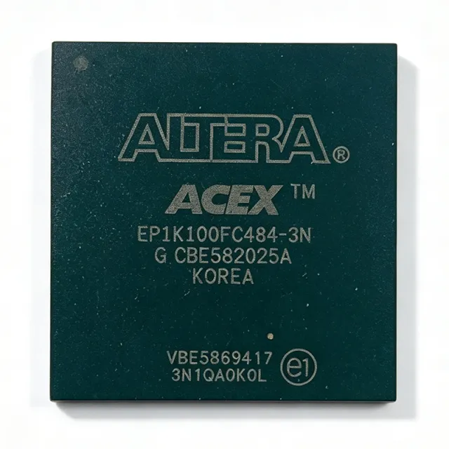
EP1K100FC256-2N
EP1K100FC256-2N - 100K-Gate ACEX FPGA | Intel
Intel EP1K100FC256-2N is a 2.5 V ACEX 1K field-programmable gate array offering approximately 100K gates, 4,992 logic cells, a 0.22 µm CMOS process, 186 user I/Os, and a listed 250 MHz maximum frequency. It is housed in a 256-pin fine-pitch BGA package and is specified with 0.5 ns loadable-PLD delay in one retrieved source. The architecture targets programmable logic integration where configurable logic, embedded memory, and interface functions must coexist in a single device.
A field-programmable gate array is a semiconductor device containing programmable logic blocks, routing resources, and configurable I/O cells. FPGA is a type of programmable logic device within the broader integrated-circuit hierarchy. Unlike a fixed application-specific integrated circuit, an FPGA can be configured after manufacturing, allowing designers to change logic functions, timing behavior, interfaces, and control functions without fabricating a new silicon device. ACEX 1K devices were designed as lower-cost system-on-a-programmable-chip platforms for implementing digital functions, memory blocks, and specialized logic.
The retrieved specifications identify 4,992 cells, 49,152 bits of RAM, 624 logic array blocks, and 186 I/Os. The device is described as a 100K-gate ACEX 1K family member using 0.22 µm technology and a 2.5 V supply. A 250 MHz frequency figure is listed by distributor and datasheet-index sources. The BGA-256 package provides dense high-count connectivity for digital systems, while the FPGA architecture supports post-assembly logic changes and design revisions.
The part uses a CMOS programmable-logic architecture with configurable logic and routing resources. The verified data describes dual-port memory functionality within the ACEX 1K family, making embedded array blocks useful for FIFOs, registers, buffers, and control state. The 0.5 ns value is presented as a loadable-PLD specification, while the 250 MHz value is a listed device frequency; these figures should not be treated as interchangeable timing guarantees for every design path. Static timing analysis and the selected I/O configuration remain necessary.
Typical applications include industrial control logic, communications-interface processing, test equipment, embedded control, and legacy digital systems requiring programmable state machines or datapaths. The 186-I/O count supports multiple buses and peripheral interfaces, while the 49,152-bit RAM resource supports localized buffering. The 100K-gate capacity is appropriate for moderate logic integration but should be compared with modern FPGA resources when migration is considered.
Designers should verify the exact ball map, configuration method, voltage requirements, timing model, and obsolete-part status from the manufacturer data before new production. For a replacement, prioritize a device with the same 256-ball footprint, compatible configuration interface, and verified pinout; a same-package mark alone is not sufficient. The page also compares the -2N device with the -3N speed-grade option, whose timing characteristics differ.
This product page synthesizes the supplied manufacturer-oriented and distributor specifications, package information, pricing snapshot, lifecycle caveats, and drop-in-oriented comparison context. It is intended as an engineering reference, not a substitute for the original ACEX 1K family datasheet, package drawings, and device-specific qualification records.
RFQ
צור קשר