מעגלי ממשק
תת-קטגוריות
מוצרים (320+)

TIOL221RGER - Dual-Channel IO-Link PHY, LDO, SPI | Texas Instruments
The Texas Instruments TIOL221RGER is a dual-channel IO-Link device physical layer (PHY) transceiver integrating two low-power output drivers with active reverse polarity protection, an integrated LDO, and an SPI interface in a 24-pin VQFN (4x4 mm) package. It provides a complete physical layer for IO-Link communication over a three-wire interface for industrial sensors and actuators. An IO-Link transceiver is a specialized interface IC that bridges a local microcontroller to the IO-Link communication standard, enabling point-to-point communication between sensors or actuators and an IO-Link master. It converts MCU digital data into IO-Link physical layer signals on the CQ line and vice versa while adding power management and protection. In the component hierarchy it sits as: IO-Link PHY -> industrial communication interface -> sensor interface IC -> mixed-signal semiconductor. Key features include dual-channel operation for two independent IO-Link ports in one package, an integrated LDO that simplifies power design, SPI-based configuration and diagnostics, and wake-up support: the device can sink or source at least 500 mA for the wake-up duration (typically 80 microseconds) depending on the CQ logic level, then asserts the WU pin low for tWUL to notify the local MCU. Surge robustness reaches 1.2 kV (500 ohm) per IEC 61000-4-5. Technically, the TIOL221 provides fault reporting and internal protection for undervoltage, overcurrent, and overtemperature conditions, and can be configured to generate wake-up pulses, also supporting IO-Link master applications. An auxiliary DI channel adds digital input functionality. Active reverse polarity protection removes the need for external series diodes, reducing voltage drop and bill-of-material cost. Typical applications include industrial proximity, pressure, and temperature sensors, actuators, and IO-Link master port circuitry. The dual-channel capability halves board area versus two single-channel PHYs. Design tip: decouple the integrated LDO carefully and configure wake-up timing per the IO-Link specification; external TVS diodes may still be needed for surge levels beyond the built-in protection.

TJA1022T - Dual LIN 2.2A Transceiver | NXP Semiconductors
The NXP Semiconductors TJA1022T is a dual LIN transceiver that interfaces a Local Interconnect Network leader or follower protocol controller with the physical LIN bus. It supports LIN bus data rates up to 20 kBd and complies with LIN 2.0, LIN 2.1, LIN 2.2, LIN 2.2A, and SAE J2602. The device is supplied in the 14-pin SO14 surface-mount package identified by the TJA1022T ordering code. A LIN transceiver is a physical-layer interface IC within the broader automotive networking hierarchy. It connects a host microcontroller or LIN protocol controller to a low-speed, single-wire vehicle network by translating controller-side logic signals into LIN bus levels and receiving bus signals for the controller. Two integrated transceivers allow one controller to manage two LIN channels while retaining a common device footprint and application architecture. The TJA1022 is primarily intended for in-vehicle subnetworks operating at baud rates up to 20 kBd. Its stated compliance includes LIN 2.0, LIN 2.1, LIN 2.2, LIN 2.2A, and SAE J2602. These protocol and automotive-interface specifications make the TJA1022T relevant to distributed vehicle systems in which body, comfort, lighting, seat, door, and other accessory modules exchange commands and diagnostic information over LIN networks. The NXP datasheet identifies the TJA1022T and TJA1022TK as pin-compatible with the TJA1020, TJA1021, TJA1027, and TJA1029. It also states that the TJA1022, TJA1024, TJA1027, and TJA1029 are software compatible. These compatibility statements support platform reuse, although designers should still verify operating conditions, enabled features, electrical limits, and package dimensions for each selected order code before treating a part as a replacement. Typical uses include vehicle body-control modules, door and seat controllers, lighting controllers, climate-control interfaces, sensor nodes, and gateway modules that combine LIN communication with microcontroller processing. The dual-channel configuration can simplify boards that must connect multiple LIN subnets while reducing the number of separate physical-layer transceivers required. When designing around the TJA1022T, preserve the pin compatibility and protocol expectations of the selected TJA1020, TJA1021, TJA1027, or TJA1029 reference design. The LIN bus interface must be reviewed against the manufacturer datasheet for termination, wiring, protection, grounding, and application-specific guidance. This page combines verified manufacturer information, distributor availability, package details, and compatibility options for faster component selection. This product data adds practical context beyond basic catalog listings by organizing protocol compliance, package compatibility, verified alternative families, bus-focused applications, and sourcing information. It highlights where the TJA1022T fits in a LIN network while clearly separating verified facts from specifications that still require confirmation from the manufacturer datasheet.

TJA1042 - 5 Mbit/s High-Speed CAN FD Transceiver | NXP
The NXP Semiconductors TJA1042 is a high-speed CAN transceiver that provides the interface between a CAN protocol controller and the physical two-wire CAN bus. It implements the CAN physical layer as defined in ISO 11898-2:2016 and SAE J2284-1 to J2284-5, supporting reliable communication in the CAN FD fast phase at data rates up to 5 Mbit/s. The typical orderable version, TJA1042T/3,118, comes in an 8-pin SOIC package. A CAN transceiver is the physical-layer device that converts controller TXD/RXD logic levels into differential bus signals (CANH/CANL) and back. Within the interface IC hierarchy, it sits between the microcontroller CAN peripheral and the bus wiring, and is essential for robust automotive and industrial networking in electrically noisy environments. Key features include a Standby mode with very low current consumption for always-on, wake-on-CAN applications; undervoltage detection on VCC; a SPLIT pin that stabilizes the recessive bus level on long networks; improved slope control; and high DC handling capability on the bus pins. As a third-generation NXP transceiver, the TJA1042 combines the functionality of the PCA82C250, PCA82C251 and TJA1040 with improved EMC and ESD performance and lower quiescent current. Thermal shutdown protection and wide supply tolerance further increase robustness. Architecturally, the TJA1042 uses a differential transceiver core with integrated common-mode stabilization and slope control, meeting demanding automotive EMC requirements without external filtering in most designs. Typical applications include automotive body control modules, gateway modules, engine control units, and industrial automation systems requiring standards-compliant CAN or CAN FD communication. Standby mode directly benefits nodes that must wake on bus activity while minimizing sleep current. Design tip: terminate the bus with 120 ohms at each end, keep the transceiver close to the connector to minimize stub length, and follow NXP application hint document AH1308 for SPLIT-pin usage to improve signal integrity on long bus lines.
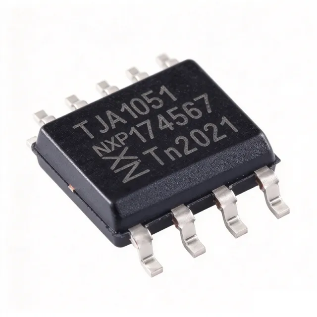
TJA1051T/3/1 - 1Mbit/s High-Speed CAN Transceiver | NXP
The NXP TJA1051T/3/1 is a third-generation high-speed CAN transceiver providing the interface between a CAN protocol controller and the physical two-wire CAN bus. It supports data rates up to 1 Mbit/s for classical CAN and CAN FD networks, operates from a 4.5V to 5.5V supply, and is packaged in an 8-pin SOIC (SO-8) surface-mount package. A CAN transceiver is a physical-layer device that converts TXD/RXD logic signals from a CAN controller into differential signals on the twisted-pair bus and back. Within the interface IC hierarchy it sits between the protocol controller and the bus, providing drive capability, bus protection, and noise immunity for reliable communication in harsh automotive and industrial environments. Key features include a VIO pin (the /3 suffix) enabling direct interfacing to 3V-to-5V microcontroller I/O rails, ideal passive behavior to the bus when unpowered (the off node does not load the network), and a silent-mode S pin that disables the transmitter while the receiver stays active. The /1 suffix indicates dual fab-site sourcing for supply-chain flexibility. The TJA1051 improves ElectroMagnetic Compatibility (EMC) and ElectroStatic Discharge (ESD) performance versus the earlier TJA1050 generation, and is AEC-Q100 qualified for automotive reliability. It is pin-compatible with the TJA1050, enabling drop-in replacement in existing layouts - note pin 5 changes from Vref output on TJA1050 to VIO input on /3 variants. Typical applications include body control modules, gateway modules, engine control units, and industrial automation networks. Low power consumption and robust ESD ruggedness suit battery-powered and harsh-environment nodes. Design tip: terminate the bus with 120 ohms at both ends and connect VIO to the microcontroller supply to match TXD/RXD/S logic levels; in 5V-only systems the non-/3 TJA1051T with pin 5 NC is also safe.

TJA1081GTS/0Z - FlexRay Node Transceiver Clamp 30 | NXP
The NXP TJA1081GTS/0Z is a FlexRay node transceiver (Clamp 30) compliant with the FlexRay Electrical Physical Layer specification ISO 17458-4:2013, supporting communication from 2.5 Mbit/s to 10 Mbit/s in a 16-SSOP package. It provides an advanced interface between the FlexRay protocol controller and the physical bus in automotive in-vehicle networks. A FlexRay transceiver is a physical-layer interface IC that converts the digital protocol signals of a FlexRay communication controller into the differential bus signals defined by the FlexRay electrical physical layer. In the vehicle networking hierarchy, it sits between the protocol controller (host MCU) and the twisted-pair FlexRay bus, forming part of the broader family of automotive network transceivers that also includes CAN, LIN and Ethernet PHY devices. FlexRay delivers deterministic, fault-tolerant, high-bandwidth communication for safety-critical and x-by-wire systems. Key features include full compliance with ISO 17458-4:2013, dual-channel differential bus drivers and receivers, and enhanced low-power modes that are optimized for ECUs permanently connected to the battery. The Clamp 30 variant is specifically intended for nodes that remain powered from the car battery at all times, integrating protection behavior suited to always-battery-connected applications. Technically, the TJA1081G implements the Bus Driver and Bus Receiver functions of the FlexRay physical layer with integrated transmit data, receive data and enable interfaces to the protocol controller. Its advanced power-management modes reduce quiescent current in standby while allowing the node to wake on bus activity, an essential property for body and chassis ECUs that draw power from Clamp 30 (battery terminal 30) even when the vehicle is parked. Typical applications include chassis control modules, adaptive suspension and x-by-wire domains, advanced driver assistance system (ADAS) gateways, and powertrain ECUs that require the deterministic 10 Mbit/s communication that FlexRay provides over CAN-based networks. A key design consideration is supply architecture: because the Clamp 30 variant is optimized for battery-permanent connection, the designer must verify the VBAT and VCC sequencing and the wake-up pin handling against the OEM electrical requirements. Always follow the manufacturer datasheet external component recommendations for the bus pins. This page synthesizes distributor availability data, family cross-references, and drop-in alternative analysis not consolidated in the manufacturer datasheet.

TJA1083GTT/0Z - FlexRay Clamp 15 Transceiver | NXP
The NXP Semiconductors TJA1083GTT/0Z is a FlexRay node transceiver (Clamp 15 type) compliant with the FlexRay Electrical Physical Layer specification ISO 17458-4:2013 (V3.0.1), housed in a 14-pin TSSOP surface-mount package, supporting communication systems operating at data rates between 2.5 Mbit/s and 10 Mbit/s. A FlexRay node transceiver is a specialized interface device that connects a FlexRay protocol controller to the vehicle's FlexRay differential bus. As a sub-category of line drivers/receivers in the automotive in-vehicle networking hierarchy (transceiver -> bus interface IC -> automotive networking IC -> semiconductor), it translates the controller's logic-level transmit data into differential bus signals and recovers received data for the controller. The FlexRay standard is used in time-triggered, fault-tolerant x-by-wire and chassis systems in modern vehicles. The TJA1083G implements the 'Increased voltage amplitude transmitter' functional class to meet JASPAR requirements, giving it enhanced differential output amplitude compared to standard-class transmitters. As a Clamp 15 transceiver, it is optimized for applications that are switched off by the ignition key, providing low-current standby behavior suited to ignition-controlled nodes. The device provides an advanced interface between the protocol controller and the physical bus, with independent receive paths for robust operation on the FlexRay channel. Technically, the TJA1083G integrates the bus driver, differential receiver, and protection circuitry needed to meet the electrical physical layer defined by ISO 17458-4:2013, including balanced-line signaling and common-mode robustness for the harsh automotive EMC environment. The /0Z ordering suffix denotes the NXP standard product grade and packaging option for this family. Typical applications include FlexRay nodes in x-by-wire chassis systems, advanced driver assistance (ADAS) domain controllers, suspension and steering systems, and gateway ECUs that bridge FlexRay, CAN, and LIN networks, where 10 Mbit/s throughput and deterministic timing are required. A key design consideration: because this is a Clamp 15 device intended for ignition-switched nodes, verify that your power-down strategy matches the Clamp 15 behavior; systems with continuous battery connection should evaluate the Clamp 30 variant of the family instead. This page synthesizes distributor pricing (as of 2026-09-13), drop-in alternatives, design notes, and application guidance not found on the manufacturer product page alone.

TJA1085GHN/0Z - FlexRay Active Star Coupler 4-Branch | NXP
The NXP Semiconductors TJA1085GHN/0Z is a FlexRay active star coupler that connects up to 4 branches of a FlexRay vehicle network, housed in a 44-pin HVQFN (9x9 mm) package. It is compliant with the FlexRay electrical physical layer specification V3.0.1 and ISO 17458-4, providing the signal regeneration and galvanic branch isolation required in fault-tolerant automotive x-by-wire and advanced driver assistance backbone networks. An active star coupler is a network topology device that receives signals on one branch, regenerates them, and retransmits them on the remaining branches. Unlike passive coupling, active star topology means a short circuit or fault on one branch does not disable the entire FlexRay bus, because the coupler electrically decouples each branch. In the automotive in-vehicle networking hierarchy, the TJA1085G sits at the physical-layer level above simple linear bus transceivers, serving as the backbone node of safety-critical, time-triggered communication systems. Key features include support for 4 FlexRay branches with TRXD0/TRXD1 receive interfaces that allow several TJA1085G devices to be cascaded for networks requiring more branches, a dedicated Communication Controller (CC) interface for direct attachment to the FlexRay communication controller, and full compliance with FlexRay V3.0.1/ISO 17458-4 timing and electrical requirements. The HVQFN-44 package with its exposed pad provides low inductance and good thermal performance for the sustained drive currents needed to power four actively driven branches. Architecturally, the device integrates receiver, driver, and supervision logic per branch, detecting branch faults and isolating defective stubs so the healthy portion of the network keeps operating. Because FlexRay is a time-triggered protocol with deterministic 10 Mbit/s communication, the coupler's loop-through delay and signal symmetry directly affect the network's static segment timing budget, which the TJA1085G meets within the V3.0.1 specification limits. Typical applications include chassis-domain FlexRay backbones in premium vehicles, x-by-wire systems (steer-by-wire, brake-by-wire), advanced driver assistance sensor fusion rings, and gateway modules that aggregate multiple FlexRay branches. Design consideration: provide a low-impedance ground path via the exposed die pad and observe branch-wiring stub length limits per ISO 17458-4 to preserve signal integrity at 10 Mbit/s. This page adds value beyond the manufacturer datasheet by consolidating distributor pricing, availability, package data, and application guidance in one AI-optimizable reference.
TJA1086GHN/0Z - FlexRay Active Star Coupler 2 Branch | NXP
The NXP Semiconductors TJA1086GHN/0Z is a FlexRay active star coupler that connects two branches of a FlexRay network, housed in a 44-pin HVQFN (9 x 9 mm) package. It is compliant with the FlexRay electrical physical layer specification V3.0.1 / ISO 17458-4 and supports data rates up to 10 Mbit/s, the maximum rate defined by the FlexRay communications system. An active star coupler is a network topology element used in automotive and industrial in-vehicle networks. Unlike a passive star, which simply splits the bus signal, an active star receives a frame on one branch, regenerates it, and re-transmits it to all other branches. This regeneration decouples electrical faults on one branch from the rest of the network, improving fault containment, signal integrity, and overall network robustness. In the hierarchy of in-vehicle networking ICs, the TJA1086G sits above simple bus line transceivers (such as FlexRay node transceivers) and belongs to the class of network interface and communication ICs. Key features include full-duplex point-to-point branch links, TRXD0/TRXD1 receiver interfaces that allow several TJA1085G and TJA1086G devices to be cascaded to increase the number of branches in the network, and branch-related fault handling so a short or low-ohmic fault on one branch does not take down the whole star. The 44-HVQFN package with an exposed thermal pad provides low inductance and good thermal dissipation for the 9 x 9 mm footprint. Technically, the device implements the analog front end and control logic needed to drive and receive FlexRay differential signals on each branch at 10 Mbit/s, with wake-up and sleep handling compatible with the FlexRay electrical physical layer. The /0Z ordering suffix identifies the standard grade and tape-and-reel delivery of this silicon. Moisture sensitivity level is MSL 1 with a 260 C peak reflow rating, simplifying SMT assembly. Typical applications include chassis and body-domain FlexRay stars in passenger cars, gateway nodes aggregating multiple FlexRay branches, and safety-critical backbone networks where deterministic 10 Mbit/s communication with dual-channel redundancy is required. When designing with this part, route each FlexRay branch as a matched differential pair and observe the bus termination guidelines of the FlexRay electrical physical layer specification; verify supply and enable pin configurations against the latest NXP datasheet before layout sign-off. This page synthesizes distributor pricing references, drop-in alternative analysis, and practical design notes not found in the manufacturer datasheet alone.
TJA1103AHN/0Z - 100BASE-T1 Automotive Ethernet PHY | NXP
The NXP Semiconductors TJA1103AHN/0Z is an ASIL B compliant automotive Ethernet 100BASE-T1 PHY transceiver with MII/RMII/RGMII MAC interface support, delivered in a 36-pin HVQFN package measuring 6 x 6 mm with exposed pad and wettable flanks. It provides 100 Mbit/s transmit and receive capability over a single unshielded twisted pair with cable lengths up to 15 m. An automotive Ethernet PHY (physical layer transceiver) is the device that converts digital MAC frames into analog signals suitable for transmission over twisted-pair cabling. Within the vehicle network hierarchy - ECU to MAC to PHY to connector - the PHY is the critical boundary component, and 100BASE-T1 (formerly OPEN Alliance BroadR-Reach) is the dominant in-vehicle networking standard, defined for automotive use in IEEE 802.3 Clause 96. Key features include IEEE 802.3 Clause 96 compliance, AEC-Q100 Grade 1 qualification (-40 C to +125 C ambient), ISO 26262 ASIL-B compliance, and OPEN Alliance TC-10 compatible sleep/wake-forwarding for low-power bus management. The TJA1103A variant carries the standard MII/RMII and RGMII(-ID) MAC interfaces, while the sibling TJA1103B variant provides an SGMII interface. On the technical side, the TJA1103 is the third generation of NXP's 100BASE-T1 automotive Ethernet PHY family. It includes integrated adaptive receive equalization, supports IEEE 1588v2 and 802.1AS-2020 2-step timestamping for time-sensitive networking, and passes all state-of-the-art conformance test specifications. Pin strapping via 3-level CONFIG pins sets critical configuration data at start-up or reset. Typical applications include edge network nodes such as camera modules and sensor ECUs, domain and zonal controllers in the center of the car, and gateway systems bridging CAN, LIN, and Ethernet domains. Design consideration: supply the PHY with its required 1.1 V, 2.5 V, and 3.3 V rails and follow NXP's layout guidance for the magnetics-free 100BASE-T1 differential pair to preserve signal integrity. This page synthesizes distributor pricing, drop-in same-family alternatives, and practical design notes not found in the manufacturer datasheet alone. Pricing data as of 2026-10-19.
TJA1104AHN - MACsec ASIL B 100BASE-T1 Automotive PHY | NXP
The NXP Semiconductors TJA1104AHN is a MACsec-enabled, ASIL B compliant automotive Ethernet 100BASE-T1 PHY transceiver with MII, RMII and RGMII MAC interface support, housed in a 36-pin HVQFN package with exposed pad (suffix /0J tape-and-reel ordering code TJA1104AHN/0J). A 100BASE-T1 PHY (physical layer transceiver) is the device that converts the digital media access controller (MAC) data of an automotive Ethernet controller into a single unshielded twisted-pair signal per IEEE 802.3bw (100 Mbit/s over one pair). Within the in-vehicle network hierarchy, the PHY sits between the switch or microcontroller MAC and the automotive Ethernet wiring harness, making it a foundational element of zonal and domain controller architectures. Key features include hardware-based MACsec (IEEE 802.1AE) link-layer security, making the TJA1104 the first MACsec-enabled device in NXP's 100BASE-T1 automotive PHY family; functional safety design according to ISO 26262 meeting ASIL B; and OPEN Alliance TC-10 compliant wake-up forwarding over the Ethernet data line for low-power sleep architectures. The TJA1104 complies with state-of-the-art conformance test specifications and provides enhanced monitoring and diagnostic features, supporting safety-critical domains such as ADAS sensor fusion, front cameras, and central gateway controllers where in-vehicle network security and functional safety must coexist. Typical applications include secure automotive Ethernet backbones, gateway ECUs, ADAS camera and radar modules, and zonal controllers that require MACsec encryption without a separate security companion chip. Design consideration: the TJA1104 is pin-to-pin drop-in compatible with the TJA1103 and TJA1120, allowing platform designs to scale security levels without PCB respin; verify MACsec-specific supply and reference-clock requirements against the manufacturer datasheet. This page synthesizes distributor availability data, NXP drop-in compatibility statements, alternatives analysis, and design guidance not consolidated in the manufacturer datasheet. Pricing shown as of 2026-10-19 where available.

TJA1104AHN-0J - MACsec ASIL B 100BASE-T1 PHY | NXP
The NXP Semiconductors TJA1104AHN/0J is a MACsec-enabled, ASIL B compliant automotive Ethernet 100BASE-T1 PHY transceiver with MII, RMII and RGMII MAC interface support, housed in a 36-pin HVQFN package with exposed pad. An Ethernet PHY (physical layer transceiver) is the interface device that converts digital MAC frames into analog signals suitable for transmission over a physical medium. In the automotive Ethernet hierarchy, the PHY sits between the media access controller (MAC) inside a processor or switch and the single unshielded twisted-pair link defined by the 100BASE-T1 standard (formerly known as BroadR-Reach), enabling in-vehicle networks to carry 100 Mbit/s data over a single pair with weight and cost savings compared with legacy 100BASE-TX. Key features include IEEE 100BASE-T1 compliant single-pair operation, hardware-based MACsec (IEEE 802.1AE) link security for protection against spoofing and man-in-the-middle attacks, and functional-safety design according to ISO 26262 to meet ASIL B with enhanced monitoring and diagnostic features. The device also integrates OPEN Alliance TC10-compliant wake-up forwarding over the Ethernet data line, enabling seamless sleep/wake coordination in automotive domain and zonal architectures. According to NXP, TJA1104 is the first MACsec-enabled product in NXP's family of 100BASE-T1 automotive Ethernet PHYs, addressing security concerns for future vehicle networks with an efficient hardware-based solution. The device complies with all state-of-the-art conformance test specifications and supports scalable platform designs: TJA1104 is drop-in compatible with TJA1103 and TJA1120, allowing designers to migrate to secured links without PCB redesign. The part is AEC-Q100 qualified for automotive environments and RoHS compliant. Typical applications include automotive domain controllers and zonal gateways requiring MACsec-secured links, ADAS sensor aggregation over in-vehicle networks, and infotainment backbones where data integrity and functional safety are critical. When designing with this device, verify MAC interface selection (MII/RMII/RGMII) early since it affects processor compatibility and reference clock architecture, and plan for TC10 wake/sleep signaling per the OPEN Alliance specification. This page synthesizes distributor pricing, drop-in alternatives, and practical design notes not found in the manufacturer datasheet.
TJA1145ATK - CAN FD Partial Networking Transceiver | NXP
The NXP TJA1145ATK is a high-speed CAN transceiver with CAN FD support and ISO 11898-2:2016 compliant partial networking, delivering 5 Mbps signaling in a 14-pin HVSON (3x4.5 mm) package with exposed pad, qualified to AEC-Q100 for automotive use. A CAN transceiver is the physical-layer device that converts the digital TXD/RXD signals of a CAN protocol controller into the differential signals on the two-wire CAN bus (CANH/CANL). Within the vehicle network hierarchy, it sits between the microcontroller's CAN controller and the bus wiring, and in partial-networking systems it also acts as a gatekeeper that wakes sleeping ECUs only when relevant messages appear. Key features of the TJA1145A family include very low power consumption in Standby and Sleep modes, a selective wake-up function that filters bus traffic so only qualifying CAN frames trigger a wake, and an integrated system-basis-chip style feature set covering INH, WAKE and reset supervision. Operating modes span Normal, Standby, Sleep, Off and Overtemp, giving designers deterministic power-state control. Technically, the transceiver provides differential transmit and receive capability for both classical CAN and CAN FD data frames up to 5 Mbps, with driver and receiver stages designed to meet the signaling symmetry and receiver timing requirements of ISO 11898-2:2016. The exposed-pad HVSON-14 package provides low loop inductance and a thermal path for the ground reference, supporting the tight bit-timing margins demanded by CAN FD arbitration and data phases. Typical applications include automotive body control modules, gateways, air-conditioning and door ECUs, and battery management nodes - anywhere a low-duty-cycle ECU must remain mostly asleep yet wake on specific bus frames. Selective wake dramatically cuts quiescent current in vehicles with large CAN clusters. Design consideration: the device is powered from VCC with I/O level adaptation via VIO, so level compatibility with 3.3 V and 5 V microcontrollers must be confirmed against the datasheet electrical characteristics before finalizing the interface. This page synthesizes distributor data, family cross-references, and practical design notes beyond the bare manufacturer datasheet, following verified web sources as of 2026-09-13.
TJA1145ATK-0Z - CAN Transceiver Partial Networking | NXP
The NXP Semiconductors TJA1145ATK-0Z is a high-speed CAN transceiver for partial networking, providing an interface between a CAN protocol controller and the physical two-wire CAN bus at data rates up to 5 Mbps, supplied from a 5V rail in a 14-pin HVSON (3x4.5 mm) package with exposed pad. A CAN (Controller Area Network) transceiver is a physical-layer interface IC that converts the single-ended TX and RX logic signals of a microcontroller's CAN controller into the differential signaling required on the twisted-pair CAN bus. Within the vehicle networking hierarchy, it sits between the protocol controller and the bus line, and belongs to the broader family of line drivers, receivers, and transceivers used in in-vehicle networking. Key features of the TJA1145ATK/0Z include support for CAN FD frames at data rates up to 5 Mbps, multiple operating modes (Normal, Standby, Sleep, Off, and Overtemp protection), and partial networking support that allows selectively woken ECUs on a partially networked bus via the dedicated WAKE pin and INH output. The device is AEC-Q100 qualified for automotive applications and supplied in tape and reel packaging. Technically, the transceiver provides differential transmit and receive capability to a microcontroller over the two-wire CAN bus, with integrated bus-side protection and an inhibit function (pin INH) that controls the external voltage regulator during low-power modes. In Off mode the CAN pins and pin INH are in a high-ohmic state, and above the power-on threshold Vth(det)pon the device boots up and enters Standby mode after tstartup, per the NXP TJA1145A datasheet. Typical applications include automotive body control modules, gateway ECUs handling partial networking wake/sleep distribution, tire pressure monitoring and battery management nodes, and any CAN FD node in vehicles requiring selective wake-up to reduce overall system current consumption. Designers should observe the 5V VCC supply requirement and ensure the mode sequencing (Standby to Normal transitions) matches the wake pattern configuration, as incorrect wake filter settings can prevent selective wake-up in partial networking systems. This page synthesizes distributor availability data, drop-in alternatives, and practical partial-networking design considerations not consolidated on the manufacturer product page.
TJA1145ATK/FD/0Z - 5 Mbit/s CAN FD Partial Networking Transceiver | NXP
The NXP Semiconductors TJA1145ATK/FD/0Z is a high-speed CAN transceiver with partial networking that provides the interface between a CAN protocol controller and the physical two-wire CAN bus, supporting CAN FD data rates up to 5 Mbit/s in a 14-pin HVSON (3x4.5 mm) package with exposed pad. A CAN (Controller Area Network) transceiver is a physical-layer device that converts the logic-level TX and RX signals of a CAN controller into the differential signals on the twisted-pair CAN bus. Within the automotive electronics hierarchy, it sits between the microcontroller CAN protocol controller and the bus lines, forming part of the broader in-vehicle networking interface family that includes LIN, FlexRay and Ethernet PHYs. Key features include full ISO 11898-2 (2016) compliance, reliable communication in the CAN FD fast phase at data rates up to 5 Mbit/s, and a dedicated partial networking implementation with the 'FD-passive' function, which allows the node to ignore CAN FD frames while waiting for a valid wake-up pattern in Sleep or Standby mode. This dramatically reduces system-level quiescent current in parked vehicles. The TJA1145A architecture integrates the transceiver, a system-basis chip function with sleep/standby/normal operating modes, local and bus wake-up recognition, and selective wake-up with CAN frame filtering. Supply voltage is specified from 4.5 V to 5.5 V, and the operating temperature range covers -40 C to +150 C, supporting under-hood and body-control deployments. Typical applications include gateway modules, body control modules, telematics units and domain controllers in automobiles, where partial-networking wake-up and CAN FD bandwidth are both required. The /0Z ordering suffix denotes the lead-free, RoHS-compliant tape-and-reel packing option. When designing with this device, always confirm pin-level compatibility before substituting other TJA1145 variants, because SO14 (T suffix) and HVSON (TK suffix) footprints differ. This page synthesizes distributor availability, drop-in alternatives, and practical design notes not found in the manufacturer datasheet.

TJF1051T/3 - High-Speed CAN Transceiver 8-SO | NXP
The NXP Semiconductors TJF1051T/3 is a high-speed Controller Area Network (CAN) transceiver that implements the ISO 11898-2:2016 physical layer, providing the physical medium interface between a CAN protocol controller and the differential CAN bus. Packaged in an 8-pin SO (SOIC-8), the part delivers up to 1 Mbps classic CAN data rate and supports CAN FD (Flexible Data-rate) frames in networks where higher payload bandwidth is required. A dedicated VIO supply pin on TJF1051T/3 lets the digital pins (TXD, RXD, S) interface directly to microcontrollers powered from 3.3 V, 1.8 V, or 5 V rails without external level shifters. A CAN transceiver is a physical-layer interface IC that converts the single-ended transmit/receive logic of a CAN controller into the differential dominant/recessive signaling used on the CAN bus, while also providing bus fault protection, ESD tolerance, and common-mode rejection. Within the broader system hierarchy, the CAN transceiver sits between the protocol controller (typically a microcontroller with a CAN module) and the wired bus; it is a member of the in-vehicle networking IC category under power management and interface functions. Compared to lower-speed LIN or RS-485 transceivers, CAN parts like the TJF1051T/3 emphasize deterministic real-time behavior, multi-node arbitration, and automotive-grade robustness. Key features include a low-current standby and silent mode with wake-up capability, ±8 kV HBM ESD on the bus pins, ±36 V bus fault tolerance on CANH/CANL, and an integrated VIO level shifter. The device operates over the automotive -40 °C to +125 °C junction range and meets the EMC and transient requirements defined by ISO 11898-2:2016. The architecture combines a low-drop voltage regulator for the VIO domain, a differential driver with controlled slew rate, and a high-CMRR differential receiver. Internal thermal shutdown protects against bus short-to-battery or short-to-ground events, and the Silent mode (S pin) lets the controller put the part into a low-Iq state without losing bias on the bus. Common applications include automotive body control modules, CAN gateway nodes, industrial CAN-FD sensor hubs, and any MCU-based system that needs an ISO 11898-compliant differential bus driver. A typical design routes TXD/RXDC straight into a STM32 or S32K microcontroller CAN module with VIO tied to the MCU's logic rail. The primary design consideration is bus termination: place 120 Ω termination at each end of the bus and keep the split stub to the TJF1051T/3 short to preserve signal integrity at 1 Mbps and above. Decoupling on VCC and VIO with 100 nF ceramic capacitors placed within a few millimeters of the pins is required for EMC compliance. This page aggregates distributor pricing, drop-in-compatible alternative part numbers, and practical EMC/layout design notes that go beyond the manufacturer datasheet summary, helping engineers select, source, and qualify the TJF1051T/3 with confidence.
TJF1103 - Industrial 100BASE-T1 Ethernet PHY | NXP
The NXP TJF1103 is a third-generation industrial Ethernet physical layer (PHY) transceiver delivering 100 Mbit/s transmit and receive capability over unshielded twisted-pair cables with support for cable lengths of up to 15 m, housed in an HVQFN package. It complies with the 100BASE-T1 single-pair Ethernet (SPE) standard. An Ethernet PHY transceiver is the physical-layer device in the OSI model hierarchy that converts the digital MAC-layer frames into analog signals suitable for transmission over copper media. Within the networking stack, the PHY sits between the media access controller (MAC) and the physical cable plant, and it belongs to the broader family of interface ICs and communication transceivers used in industrial automation, automotive networking, and edge computing systems. Key features of the TJF1103 include full compliance with state-of-the-art conformance test specifications for 100BASE-T1, design to NXP quality management (QM) requirements, enhanced monitoring and diagnostic capabilities, and a choice of MAC interfaces depending on the variant. The TJF1103A variant contains standard MII/RMII and RGMII (-ID) MAC interfaces, while the TJF1103B variant provides an SGMII interface, giving designers flexibility in connecting to a wide range of industrial processors, switches, and FPGA-based systems. Architecturally, the TJF1103 builds on NXP's successful family of 100BASE-T1 automotive Ethernet PHYs, re-targeting the proven third-generation technology for the rapid expansion of Ethernet in industrial applications. Single-pair Ethernet reduces cabling weight, cost, and connector complexity compared with four-pair 100BASE-TX, which is a decisive advantage in compact industrial nodes, sensors, actuators, and machine vision endpoints. Typical applications include industrial automation networks, single-pair Ethernet links between PLCs, drives, I/O modules and sensors, compact embedded controllers, and industrial camera or machine-vision endpoints where 15 m cable reach and low cabling cost matter. The industrial qualification focus makes it suitable for factory floor environments. A key design consideration is variant selection: choose TJF1103A when the host processor offers a parallel MII/RMII or RGMII MAC interface, and TJF1103B when a serial SGMII link to a switch fabric or SerDes-based host is required, since the two variants use different MAC interfaces. This page synthesizes distributor availability, variant cross-references, and drop-in alternative guidance not found in the manufacturer datasheet.
TLE62513GXUMA1 - 1Mbit/s HS-CAN Transceiver | Infineon
The Infineon Technologies TLE62513GXUMA1 is a high-speed half-duplex CAN transceiver designed for data rates up to 1 MBaud in a 14-pin PG-DSO-14 package. It supports a 5.5 V to 18 V transceiver supply range, includes a separately adaptable VIO input for the connected microcontroller supply voltage, and provides bus and local wake-up support. The device operates in Normal, Sleep, and Standby modes and exposes a Wake-Up Inhibit output for controlling external circuitry. Its separate failure-diagnosis output helps system designers monitor transceiver operating conditions. The TLE62513GXUMA1 is compliant with ISO 11898-5, uses a RoHS-compliant PG-DSO-14 package, and is optimized for low electromagnetic emission and high electromagnetic immunity. These characteristics make it suitable for automotive and industrial Controller Area Network nodes that require robust communication, low standby consumption, and flexible interfacing between a 5 V CAN transceiver domain and a lower-voltage microcontroller domain. A CAN transceiver, also called a CAN interface controller or CAN physical-layer transceiver, converts logic-level TXD and RXD signals into the differential dominant and recessive states used on a CAN bus. The TLE62513GXUMA1 supports high-speed CAN networks operating at up to 1 MBaud and complies with ISO 11898-5. Its half-duplex architecture allows one transceiver to share its CANH and CANL bus connections with other network nodes while using a common bus termination and protection arrangement. The principal features include a maximum 1 MBaud data rate, low power consumption in Sleep mode, bus wake-up capability, a local Wake-Up Inhibit output, and a separate VIO input. The independently adaptable VIO domain allows the TXD and RXD interface voltage to follow the MCU supply level while the transceiver supply remains independent. Normal, Sleep, and Standby operating modes support communication, power saving, and controlled wake behavior. The dedicated failure-diagnosis output provides a hardware indication of transceiver conditions for monitoring by the host controller. In electrical terms, the device separates the bus-side and logic-side functions. VCC supports the transceiver supply range of 5.5 V to 18 V, while VIO adapts the digital interface to different microcontroller supply voltages. This separation is particularly useful in mixed-voltage automotive systems, where a low-voltage MCU may communicate through a CAN physical layer supplied from a vehicle-level rail. The device's low electromagnetic-emission design reduces interference with nearby electronics, while its high immunity rating supports reliable reception in electrically noisy environments. Typical uses include 24 V automotive body, comfort, and powertrain communication networks; industrial automation controllers; distributed sensor and actuator nodes; gateway equipment; and mixed-signal embedded systems. In an automotive application, the CANH and CANL pins connect to the protected bus wiring, RXD connects to the MCU receive input, and TXD connects to the MCU transmit output. The separate VIO connection lets the logic interface operate at the MCU's supply voltage without changing the main transceiver supply. PCB design should preserve the recommended CAN bus routing, provide a common-mode choke and ESD protection where required, and place transceiver-related protection close to the connector. The bus traces should remain short and symmetric, with the 120 ohm split termination implemented across CANH and CANL. VCC and VIO need local high-frequency bypass capacitors, while ground-return paths should remain continuous. The data sheet and application information should be consulted before finalizing termination, protection, sleep-mode, and wake-up behavior. This page combines the verified TLE62513GXUMA1 product data with same-package family alternatives, practical CAN interface design guidance, and a parameter comparison intended to accelerate engineering selection and sourcing.
TLE6251GNTMA1 - 1 Mbit/s CAN Transceiver | Infineon
Infineon Technologies TLE6251GNTMA1 is a 5 V high-speed CAN bus transceiver with sleep and standby operating modes, supplied in a 14-terminal PG-DSO-14-13 surface-mount package. Verified distributor data identifies the device as a 1/1 full CANbus transceiver, while application listings describe the TLE6251 family as a high-speed CAN transceiver supporting data rates up to 1 Mbit/s. Its principal role is to connect a host controller to a CAN network through a differential transmit and receive interface. A CAN transceiver is a physical-layer interface IC within the Controller Area Network ecosystem. The broader hierarchy is CAN transceiver, CAN interface IC, bus transceiver, interface IC, and semiconductor. A CAN controller generates and interprets CAN frames, while the transceiver converts that logical information into the CANH and CANL differential bus signals required for reliable, noise-resistant communication between automotive, industrial, and embedded systems. Verified product information highlights several useful characteristics. The TLE6251GNTMA1 operates from a 5 V supply, supports a maximum CAN data rate of 1 Mbit/s, and provides sleep and standby modes for reduced power use. It is described as a full-duplex CAN interface, meaning the transceiver supports both transmission onto the bus and reception from the bus. The 14-terminal PG-DSO-14-13 package is a surface-mount gull-wing package based on the listed SOP configuration. The sleep and standby functions are central to its power-management behavior. Standby permits the device to remain available for bus-related activity, while sleep supports a lower-power network state. Exact threshold values, current consumption, loopback behavior, bus fault reporting, and timing limits should be confirmed in the Infineon manufacturer datasheet before a design is released; those detailed values were not present in the supplied verification records. TLE6251GNTMA1 is suitable for automotive control modules, body and comfort electronics, industrial automation equipment, robotics controllers, diagnostic interfaces, and embedded CAN gateways. In a typical design, a CAN controller connects to the transceiver logic pins, while CANH and CANL connect to the physical bus. Termination is normally placed at both ends of the bus rather than at every node. PCB implementation requires correct routing of the differential bus pair, a solid ground reference, suitable supply decoupling, and compliance with the isolation and termination requirements of the selected CAN network. The bus conductors should be kept as a controlled-impedance pair, with minimal stubs and branching, because connector branches and excessive trace length can degrade signal integrity at the supported 1 Mbit/s class of operation. This product record combines verified distributor identification, family-level CAN features, package information, cross-reference findings, and practical design guidance. It also distinguishes the TLE6251 family options that require datasheet-level confirmation before being treated as drop-in replacements, providing useful context beyond a distributor listing or a basic catalog entry.
TLE8457DSJXUMA1 - LIN Transceiver + 3.3V LDO | Infineon
The Infineon TLE8457DSJXUMA1 is a monolithic LIN transceiver with an integrated 3.3 V low-dropout voltage regulator, supplied in an 8-pin PG-DSO-8 (TSON-8) surface-mount package. It is a 1/1 LIN transceiver supporting LIN specification 2.2A and SAE J2602, with a maximum data rate of 20 kbps and an integrated LDO capable of sourcing up to 70 mA at 3.3 V for a host microcontroller and its sensors. A LIN (Local Interconnect Network) transceiver is a physical-layer interface IC that bridges a low-speed microcontroller UART to a single-wire automotive bus. The LIN bus is standardized in ISO 17987 and widely used for body-electronics sub-networks (door modules, mirror adjusters, seat controllers, HVAC flaps) where CAN is too expensive. The integrated LDO allows a TLE8457DSJ slave node to be powered directly from the 12 V automotive battery without a separate voltage regulator, simplifying PCB design. Key features of the TLE8457DSJXUMA1 include an ultra-low standby current of 20 µA (suitable for permanent-battery-attach nodes), battery input voltage range of 5.5 V to 28 V with transient tolerance per ISO 7637, integrated VCC undervoltage reset with fixed 3.3 V output, integrated current limit, thermal shutdown, and bus-pin ESD protection up to ±8 kV (HBM). The device operates across the automotive -40 °C to +150 °C junction temperature range and is qualified to AEC-Q100 grade 1, making it suitable for under-hood and body-control modules. The TLE8457DSJ uses a bi-directional bus driver architecture compliant with LIN 2.2A and SAE J2602, with internal slope control to meet EMC requirements per IEC 61967 and SAE J1752. The integrated LDO is a p-channel MOSFET LDO architecture for low quiescent current, with internal compensation and soft-start. The part is offered as 'DSJ' (PG-DSO-8) only — the XUMA1 suffix denotes a 2,500-piece reel per IEC 60286-3. Typical applications include LIN slave nodes in door modules, seat-control modules, HVAC damper actuators, interior lighting, rain/light sensors, and other LIN sub-nodes in automotive body-electronics networks. The integrated 3.3 V/70 mA supply removes the need for an external regulator at each LIN slave, reducing BOM count and PCB area. When designing with the TLE8457DSJXUMA1, ensure the LIN bus pull-up is correctly selected (the device provides the slave-side pull-up internally only in some modes — see the datasheet). Place the VBAT decoupling capacitor (typically 100 nF ceramic + bulk) close to the VBAT pin to meet ISO 7637-2 transient immunity. This page synthesizes distributor pricing, drop-in alternatives, and practical design notes for the TLE8457DSJXUMA1 not found in the manufacturer datasheet alone.

TLIN1027DRBRQ1 - Automotive LIN Transceiver 20kbps | TI
The Texas Instruments TLIN1027DRBRQ1 is an automotive-grade local interconnect network (LIN) physical-layer transceiver with integrated wake-up and protection features, delivering data rates up to 20 kbps on a single-wire bidirectional bus in an 8-pin VSON (DRB) 3x3 mm package. A LIN transceiver is the physical-layer interface IC that translates the logic-level signals of a microcontroller UART into the differential-dominant signaling of a single-wire LIN bus. Within the vehicle networking hierarchy, LIN sits below CAN and CAN FD as a low-cost, low-speed sub-bus for mechatronic nodes such as seat controllers, mirrors, pumps and sensors. The transceiver itself is a member of the broader family of bus interface and network transceiver ICs in power-management and interface semiconductor taxonomies. Key features include compatibility with LIN 2.0, LIN 2.1, LIN 2.2, LIN 2.2A and ISO/DIS 17987-4.2 standards, integrated wake-up via the LIN bus or the EN pin, a low-power sleep mode, and on-chip protection. The TLIN1027-Q1 variant is specified without a dominant state timeout, and the device is designed to support 12-V automotive applications with wider operating margins. Technically, the TLIN1027-Q1 integrates an internal wake-up receiver and protection structures that reduce external component count. Thermal shutdown protection guards the output driver against fault conditions on the bus, and the 8-VDFN exposed-pad package provides a low-inductance ground path important for automotive EMC performance. Typical applications include in-vehicle networking nodes such as body-control modules, door modules, seat adjusters, HVAC actuators and 12-V sensor clusters, where the 20 kbps LIN data rate and single-wire wiring harness savings fit the cost structure of these subsystems. Design consideration: because LIN drivers drive a resistive bus terminated through a 1 kOhm dominant-dominant divider, verify supply headroom and thermal shutdown thresholds against worst-case bus shorts in your fault analysis. This page synthesizes verified distributor pricing, drop-in alternatives, and practical design notes not found in the manufacturer datasheet.

TLIN10283DRBRQ1 - LIN Transceiver SBC 3.3V LDO | Texas Instruments
The Texas Instruments TLIN10283DRBRQ1 is an automotive Local Interconnect Network (LIN) physical-layer transceiver with an integrated low-dropout (LDO) voltage regulator, compliant to LIN 2.2A and ISO/DIS 17987-4 standards, operating from a 5.5V to 28V supply in an 8-pin VSON (DRB, 3x3 mm) package with up to 125 mA regulator output current. A LIN transceiver is the physical-layer interface IC that converts the UART data stream of a microcontroller into the dominant/recessive differential signaling used on a LIN bus. Within the system hierarchy, it sits between the MCU (logic domain) and the vehicle wiring harness (12V physical domain), and when combined with an LDO it forms a LIN system basis chip (SBC) - a subset of full automotive network processors. Key features include an integrated 3.3V LDO regulator delivering up to 125 mA for the local MCU or sensors, LIN 2.2A / ISO/DIS 17987-4 protocol compliance for interoperability across vehicle platforms, AEC-Q100 automotive qualification for harsh 12V environments, and low quiescent power operation with wake-up support on the LIN bus. The 3x3 mm VSON package with exposed pad enables compact ECU node designs. Technically, the device integrates the LIN line driver and receiver with stringent output slew control to meet the 20 kbps (maximum) LIN data rate while minimizing EMC emissions, plus protection features such as loss-of-ground and load-dump tolerance typical of TI LIN SBCs. The LDO eliminates an external 3.3V regulator, reducing BOM count and PCB area in each node. Typical applications include body control modules, window/seat/door zone control units, HVAC actuators, and sensor nodes distributed across a 12V automotive LIN network. A key design consideration: verify that the total current drawn by the local MCU and sensors stays within the 125 mA LDO budget, and use a large enough exposed-pad copper area for thermal dissipation in dense nodes. This page synthesizes distributor availability, drop-in alternatives, and practical design guidance not found in a single manufacturer datasheet.
TMC22053AKHC - 10-Bit 3-Line Video Decoder | onsemi
The onsemi TMC22053AKHC is a multistandard digital video decoder with 10-bit processing and three-line adaptive comb decoding, supplied in a 100-pin MQFP package measuring 20 x 14 mm. The device belongs to the TMC22x5yA decoder family, which combines multistandard color-signal decoding with multiple pin-compatible processing configurations for NTSC and PAL video systems. A digital video decoder is an interface IC that reconstructs usable luminance and chrominance information from encoded composite video signals. Within the signal-chain hierarchy, this device functions as a video decoder, then an interface IC, and ultimately a semiconductor designed for broadcast-quality video processing. Its adaptive comb-based architecture separates adjacent video information so that undesirable signal mixing can be reduced during decoding. The TMC22053AKHC provides 10-bit digital processing within the TMC22x5yA family, whose related devices include three-line, two-line, and band-split configurations with 8-bit and 10-bit options. Internal digital line stores support the decoding architecture. Its parallel and serial NTSC/PAL association, as identified by the distributor product listing, makes it suitable for legacy analog-video capture, broadcast equipment, industrial monitoring, and video-production hardware that requires a dedicated multistandard decoder. The MQFP-100 package provides 100 external connections for parallel pixel data, control signals, memory interfaces, synchronization, and power. This high pin count reflects the breadth of the legacy broadcast-video interface and its support for programmable operating modes. Because the available source material does not provide the complete electrical limits or a manufacturer pin table, voltage ranges, current consumption, clock limits, and individual pin assignments must be confirmed in the original manufacturer datasheet before schematic capture or PCB release. Typical implementation places the TMC22053AKHC between a composite-video input stage and a digital video processor or frame buffer. The decoder extracts luminance and chrominance information and presents processed data through its configurable digital interfaces. In professional monitoring equipment, broadcast test equipment, or legacy industrial camera systems, its three-line adaptive comb processing can help separate neighboring video information while retaining support for both NTSC and PAL sources. The main design consideration is not that the IC simply replaces a generic codec: it is a specialized legacy video-decoder block whose supply, clock, memory, and interface timing requirements must be implemented exactly as specified. Designers should preserve the recommended analog input network, clock topology, decoupling arrangement, and controlled-impedance digital routing. Because the exact pinout is not available in the supplied verified excerpts, the physical land pattern must be checked against the authoritative 100-pin documentation before routing. This page combines verified distributor pricing, family-level processing details, package information, application guidance, and drop-in replacement analysis. It also separates confirmed facts from parameters that remain unavailable, helping engineers plan a legacy video-decoder design without treating unsupported electrical assumptions as manufacturer specifications.
TMC22071AKHC Genlocking Video Digitizer | onsemi
The onsemi TMC22071AKHC is a genlocking video digitizer with an integrated three-channel video-input multiplexer, two-stage video clamp, automatic gain adjustment, and synchronization detection and separation in a 100-pin MQFP package measuring 20 mm by 14 mm. It supports analog NTSC and PAL video inputs, including pixel and subpixel adjustment of horizontal synchronization relative to video timing and genlocking to NTSC or PAL sources. A video digitizer is a signal-processing IC that converts analog composite-video information into digital timing and pixel-related data for subsequent processing. Within the video-processing hierarchy, it combines analog input conditioning, synchronization extraction, timing measurement, phase-locked-loop control, and a digital direct digital synthesizer. The TMC22071AKHC therefore sits between composite-video sources and downstream digital video or synchronization systems rather than functioning as a general-purpose video encoder. The verified feature set includes a fully integrated three-channel acquisition multiplexer and a two-stage video clamp. These functions allow multiple analog video inputs to share the acquisition path while stabilizing the signal before it reaches the timing-processing circuitry. Automatic gain adjustment compensates for input-level variation, and synchronization detection and separation supports reliable identification of video timing information. The operating range is specified from 0°C to 70°C. Internal timing functions include horizontal synchronization generation, pixel and subpixel HSYNC-to-video timing adjustment, a horizontal phase-locked loop, and a direct digital synthesizer. The verified pin information also identifies PLL-filter, phase-frequency-detector input, bypass-capacitor, reference-voltage, compensation, clock-input, and clock-output connections. These blocks indicate that the device performs both synchronization recovery and programmable timing generation rather than simply digitizing luminance and chrominance voltage levels. Typical uses include NTSC or PAL video timing generation, multi-source video selection, genlocking equipment, broadcast and professional video systems, laboratory video synchronization setups, and embedded systems that need repeatable timing derived from an external composite-video source. A three-channel multiplexer is particularly useful where several sources must be acquired through a shared analog front end. Designers should pay particular attention to analog grounding, bypass placement, reference and compensation networks, PLL filtering, and external clock implementation. Because this is a high-pin-count MQFP device, PCB layout should minimize analog and digital return paths while preserving the application values recommended in the manufacturer datasheet. The 0°C to 70°C specification also makes this part best suited to commercial-temperature equipment rather than extended industrial or automotive environments. This page combines verified manufacturer and distributor data with practical design context, explicit data gaps, and a same-package alternative review. It is designed to support datasheet lookup, procurement, initial circuit planning, and drop-in replacement assessment without inventing electrical ratings, pin functions, or cross-reference data that the supplied sources do not establish.
TMC22151KHC - Multistandard Video Decoder IC | Fairchild
Fairchild TMC22151KHC is a multistandard digital video decoder IC offered in a 100-MQFP surface-mount package measuring 20 mm by 14 mm. The supplied distributor records identify it as an encoder, decoder, and converter interface device, while related family information describes the TMC22151 series as a multistandard digital video decoder family. Its exact electrical limits, supported video standards, clock requirements, operating-temperature range, and pin assignments were not included in the verified source excerpts and therefore require confirmation from the manufacturer datasheet. A video decoder IC is a video-interface component that converts encoded composite or other legacy video signals into digital video data for subsequent processing, display, or recording. Within the product hierarchy, TMC22151KHC is a video decoder, a member of interface ICs, and ultimately part of the broader semiconductor and signal-processing categories. Its role is distinct from image sensors and display drivers: the decoder reconstructs digital video information from an incoming analog signal rather than capturing optical images or driving pixels directly. The verified TMC22151-family description identifies adaptive comb-based decoding, internal digital line stores, and multiple pin-compatible processing versions with 8-bit and 10-bit options. A related TMC22151AKHC listing specifically advertises a 10-bit configuration, but it does not establish that every parameter of that variant is identical to the TMC22151KHC. The 100-MQFP package provides a high pin count suitable for parallel digital data, multiple clock domains, control signaling, memory interfaces, and analog video inputs. Package dimensions of 20 mm by 14 mm are explicitly confirmed by the DigiKey listing. TMC22151KHC is associated with studio television equipment in distributor records, indicating legacy broadcast-video processing rather than general-purpose computing. Its architecture and decoded-word width must be verified before use in a new PCB because decoder variants can differ in filtering, bit depth, interfaces, and system timing. Related family listings mention three-line, two-line, and band-split processing paths, but those configurations are not conclusively tied to the exact KHC suffix without the corresponding datasheet revision. Potential uses include broadcast monitor decoding, video production equipment, industrial inspection systems, and professional video capture chains that still rely on multistandard composite video. The component may sit between an analog video input connector and downstream digital video processing, but the exact input levels, synchronization method, chroma format, and bus voltage must come from the full datasheet and application circuit. Before designing a replacement board, engineers should compare every numbered 100-MQFP connection, supply rail, clock input, and control signal against the official pinout. PCB layout should separate analog video inputs from digital outputs, provide stable decoupling, and use controlled-impedance routing where supported by the interface specification. Because the retrieved data does not establish production lifecycle, RoHS, REACH, AEC-Q100, thermal, or supply status, those attributes should be confirmed with Fairchild or onsemi. This page consolidates verified distributor pricing, package information, source links, application context, and replacement constraints for TMC22151KHC. It deliberately distinguishes confirmed facts from unavailable specifications, helping engineers identify whether the part fits a legacy video design before requesting the full datasheet or committing to a board redesign.