מעגלי ממשק
תת-קטגוריות
מוצרים (3,100+)

TCA9535DBR - 16-Bit I2C I/O Expander | Texas Instruments
Texas Instruments TCA9535DBR is a low-voltage, low-power 16-bit I2C and SMBus I/O expander with an interrupt output and configuration registers. It operates from 1.65 V to 5.5 V, supports I2C communication at up to 400 kHz, and provides 16 general-purpose parallel I/O lines in a 24-pin SSOP package. An I/O expander is an interface IC that increases the number of digital input and output pins available to a host controller. The host communicates with the TCA9535DBR through a two-wire I2C or SMBus interface, while the 16 external lines handle logic inputs, outputs, or mixed functions. In the system hierarchy, this device belongs to the interface IC family and bridges a serial control bus with parallel digital signals. The principal features are 16 independently configurable I/O pins, a 1.65 V to 5.5 V operating range, and a maximum bus frequency of 400 kHz. The interrupt output allows a connected controller to react when an input changes, reducing the need for continuous polling. Separate configuration registers support control of the direction and behavior of the I/O ports, while the device is designed for low-power operation. TCA9535DBR is packaged in a 24-pin SSOP, providing a compact surface-mount format for programmable control, monitoring, and signal-routing boards. Its I2C interface is suitable for buses that also carry configuration data or communicate with sensors, memory, and other interface devices. The 400 kHz capability allows the expander to operate on standard low-speed I2C systems without changing the host protocol. Typical applications include industrial control panels, programmable logic controllers, building automation equipment, test systems, and embedded products that require additional digital lines. The part can also expand button or switch inputs, control discrete logic signals, and provide interrupt-driven status reporting. Its small pin count relative to the number of external I/O lines helps conserve connector space and simplify system architecture. When designing around the TCA9535DBR, account for address selection, pull-up requirements, input thresholds, and the electrical characteristics of every attached signal. Confirm the board footprint and pin assignment against the manufacturer datasheet before release, especially when replacing a device with similar I/O count but different input or output polarity. The design notes and comparisons on this page provide practical guidance for firmware setup, PCB layout, and device selection.
TCA9535DBT - 16-Bit I/O Expander | Texas Instruments
The Texas Instruments TCA9535DBT is a 16-bit I/O expander for the I2C or SMBus interface, operating from a 1.65 V to 5.5 V supply at up to 400 kHz. The device provides 16 general-purpose bidirectional I/O lines, an interrupt output, and configuration registers in a 24-pin SSOP package. An I/O expander is an interface IC that increases the number of digital input and output pins available to a host controller without requiring a larger microcontroller package. The TCA9535 belongs to the I/O expander hierarchy, where a serial I2C or SMBus connection controls parallel digital lines. Its 16 ports can operate as inputs, outputs, or mixed configurations, making it useful for control panels, sensor aggregation, relay interfaces, and compact embedded systems. The main features include a wide 1.65 V to 5.5 V operating range, 16 general-purpose I/O lines, separate configuration registers, and an interrupt output. The I2C interface supports operation up to 400 kHz, while the three address inputs allow multiple devices to share the same serial bus. The interrupt output lets the connected processor respond only when a programmed input or output event occurs instead of polling every port continuously. Internally, the TCA9535 separates the 16 I/O lines into four eight-bit ports. Each port has its own configuration register, while dedicated input and output registers provide independent control of direction and data. This organization supports mixed input and output operation without requiring a separate GPIO controller for every line. Three hardware address inputs select the device address used on the shared bus. Typical applications include expanding a microcontroller's available GPIO, reading discrete switches and sensors, driving LEDs or digital control signals, implementing a keypad interface, and controlling multiple peripheral enables. The low-voltage operation also suits battery-powered and portable equipment where the host and expander operate from a 1.8 V, 2.5 V, 3.3 V, or 5 V system rail. Design the bus carefully when several expanders share SDA and SCL. Keep pull-up resistors within the range specified by the manufacturer datasheet, route the bus away from noisy switching nodes, and account for capacitance when increasing cable length or the number of devices. Decoupling close to VCC and GND improves stability in compact systems. This product page combines the manufacturer's core electrical characteristics, package and pin information, compatibility-focused alternatives, application guidance, and practical design considerations to support faster component selection and PCB planning.

TCA9535PWR - 16-Bit I/O Expander | Texas Instruments
Texas Instruments TCA9535PWR is a low-voltage 16-bit I2C and SMBus I/O expander with interrupt output and configuration registers, operating from 1.65 V to 5.5 V at up to 400 kHz and housed in a 24-pin TSSOP (PW) package. It adds 16 general-purpose parallel I/O lines to a host microcontroller or processor through a two-wire serial bus. An I/O expander is an interface IC that increases the number of digital input and output pins available to a host without requiring a large package or a dedicated parallel peripheral. The TCA9535PWR belongs to the broader I/O expander hierarchy, where each port bit can be independently configured as an input or output. Configuration, polarity-inversion, and interrupt functions make it suitable for systems that need remote control or change notification from external logic. The principal features include 16 independently configurable I/O pins, a 1.65 V to 5.5 V operating supply range, I2C/SMBus compatibility, and a 400 kHz bus rate. Separate configuration registers determine whether each port pin operates as an input with a high-impedance output driver or as an output. Polarity-inversion registers can reverse the logical interpretation of input pins, while the interrupt output provides a hardware indication of an input-state change. The two-wire interface reduces the number of host pins needed for peripheral expansion. The host writes to the configuration and polarity registers and reads port status over the serial bus. This arrangement is useful when the additional lines control relatively simple discrete functions rather than high-bandwidth data. The interrupt mechanism avoids continuous polling when a remote input or configured output state changes. Typical uses include LED and indicator control, button and switch input, relay-interface signaling, sensor-interface control, and general-purpose logic expansion in embedded products. The TCA9535PWR is particularly appropriate for low-voltage systems operating from 1.65 V through 5.5 V, including industrial control, communications equipment, consumer electronics, and programmable-logic applications. Design the power and signal path carefully. Confirm that every port-pin voltage remains within its applicable input and output limits, account for the total current drawn by simultaneously active outputs, and use pull-up resistors sized for the bus capacitance and operating speed. Treat the interrupt pin as an output signal from the expander and design firmware to clear the interrupt source before returning to normal polling. This product page combines manufacturer specifications, verified source links, pin-compatible alternatives, and application-oriented design guidance to accelerate component selection and PCB implementation. It also highlights the distinctions among device addressing and register behavior so engineers can identify the correct substitute before changing an approved design.

TCA9536-Q1 - 4-Bit I2C/SMBus I/O Expander AEC-Q100 | TI
The Texas Instruments TCA9536-Q1 is a 4-bit remote I/O expander for the I2C bus and SMBus with configuration registers, operating from a 1.65V to 5.5V supply in an 8-pin X2SON package measuring just 1.35 mm x 0.8 mm. It provides general-purpose remote I/O expansion for most microcontroller families via the I2C interface and is AEC-Q100 qualified for automotive applications. An I/O expander is an interface IC that extends the number of general-purpose input/output (GPIO) pins of a microcontroller or system controller through a serial bus such as I2C or SMBus. In the hierarchy of embedded system components, the I/O expander sits within the interface IC family, alongside level translators, bus buffers, and serial transceivers, and functions as a remote GPIO peripheral for system masters that need additional discrete control or monitoring lines without adding a larger microcontroller. Key features of the TCA9536-Q1 include 4 configurable I/O pins that can be individually programmed as inputs or outputs through a 4-bit Configuration register, an Input Port register for reading pin states, an Output Port register for driving pins, and a Polarity Inversion register for active-HIGH or active-LOW operation. The device supports fast-mode I2C bus operation up to 1 MHz, uses only two bus lines (SDA and SCL), and operates across the wide 1.65V to 5.5V VCC range for compatibility with 1.8V, 2.5V, 3.3V, and 5V logic systems. The architecture implements four 4-bit registers (Configuration, Input Port, Output Port, and Polarity Inversion) accessible over the serial bus, with power-on reset defaulting all pins to inputs. Because the TCA9536-Q1 register map follows the widely deployed PCA9536 register convention, the same software drivers used for PCA9536-class expanders generally work unchanged, simplifying migration and second-sourcing within an existing firmware stack. Typical applications include automotive body-control modules, GPIO expansion in space-constrained sensor nodes, keypad or switch monitoring, LED and relay control through external drivers, and power-rail sequencing enables in infotainment and cluster displays. Its tiny X2SON footprint makes it especially attractive where board area is the limiting factor. Design consideration: because the X2SON package places multiple pins on very fine pitch beneath the die, follow TI's recommended PCB land pattern exactly, including via-in-pad thermal relief, and verify solderability with the correct reflow profile for the Q1 automotive grade. This page synthesizes verified distributor data, drop-in alternative analysis, and practical design guidance that goes beyond the raw datasheet parameters.

TCA9538DBR - 8-Bit I2C I/O Expander | Texas Instruments
Texas Instruments TCA9538DBR is an 8-bit I2C/SMBus low-power I/O expander with a 1.65 V to 5.5 V operating range, 400 kHz bus speed, and a 16-pin SSOP package. It adds eight general-purpose input or output ports through a two-wire serial interface while providing interrupt, reset, and configuration registers. The device is intended for systems in which a host controller needs more parallel I/O than its native package or connector resources can provide. An I/O expander is an interface IC that extends the number of digital input and output pins available to a host processor. The TCA9538 belongs to the I2C interface hierarchy, where the I2C or SMBus protocol links the expander to a controller such as a microcontroller. Each port can be configured as an input or output, allowing the same circuit to support switches, sensors, logic-control signals, LEDs, and other digital peripherals while conserving host pins and reducing interconnect complexity. The principal operating parameters are an 8-bit port count, a 1.65 V minimum supply voltage, a 5.5 V maximum supply voltage, and support for a 400 kHz I2C bus. According to the Texas Instruments product page, the device also includes an interrupt output, reset control, and configuration registers. These functions support event-driven peripheral monitoring and orderly control of multiple downstream signals without continuous polling by the host processor. The TCA9538DBR is a remote, low-power parallel-interface device rather than a general-purpose processor or transceiver. Its serial control path uses the two-wire I2C or SMBus interface, while the eight parallel ports connect to digital circuitry in the target system. The SSOP-16 package provides a compact surface-mount format, and the manufacturer lists the part as active. Its operating temperature range is -40 °C to +85 °C, supporting industrial-temperature equipment when correctly handled for thermal and soldering requirements. Typical uses include control-panel backlights, sensor and switch interfaces, relay-control inputs, programmable logic interfaces, battery-powered monitoring equipment, and communication equipment requiring additional GPIO. The TCA9538 is especially useful when the host controller has limited spare pins but the system still needs eight independently configurable digital lines and an interrupt mechanism for status changes. Design the bus with pull-up resistors appropriate for the operating voltage, confirm that the 400 kHz bus rate is compatible with the complete bus capacitance and every attached peripheral, and account for logic thresholds when the expander operates alongside mixed-voltage devices. Place the interface pins, supply decoupling, and pull-up network to minimize routing delay and maintain signal integrity across the board. This product record combines the manufacturer’s electrical and package information with practical interface-selection guidance, pinout-location references, application analysis, and compatibility cautions. It also distinguishes true same-package drop-in replacements from related expanders that differ in footprint, voltage tolerance, interrupt behavior, or register implementation and therefore require engineering review before substitution.

TCA9538PWR - 8-Bit 1.65-5.5V I/O Expander | Texas Instruments
The Texas Instruments TCA9538PWR is an 8-bit I2C and SMBus I/O expander operating from 1.65 V to 5.5 V, supporting bus speeds up to 400 kHz and packaged in a 16-pin TSSOP. It adds eight general-purpose parallel I/O lines to a host microcontroller or embedded processor while providing interrupt, reset, and configuration registers. An I/O expander is a peripheral interface device that increases the number of inputs and outputs available to a central controller. Positioned between the host processor and external logic, an I2C expander uses serial control lines to configure and monitor multiple parallel ports. This expands the I2C bus > interface IC > peripheral interface > semiconductor hierarchy without requiring additional direct GPIO pins on the host. The device provides 8 configurable general-purpose I/O bits, allowing each line to function as an input or output according to the port configuration register. The TCA9538 also includes an interrupt output for input-state changes, hardware reset control, and two hardware-selectable address inputs. These features support deterministic control of sensors, relays, logic gates, indicators, and other peripheral hardware over a shared serial bus. The TCA9538 supports both 100 kHz Standard-mode and 400 kHz Fast-mode I2C operation. Its 1.65 V to 5.5 V operating range covers low-voltage embedded systems as well as 5 V industrial and commercial equipment. Two address-selection pins allow up to four TCA9538 devices on the same bus when the surrounding system has sufficient address and interrupt-routing resources. Typical applications include industrial control panels, programmable logic controllers, sensor-hub boards, motor and relay interfaces, LED status panels, and compact embedded control systems. The eight-port architecture is especially useful when a host needs additional digital lines for sensors, switches, and discrete outputs without expanding the host package. Designers should follow the manufacturer datasheet when assigning the I2C address, configuring input or output direction, selecting pull-up resistors, and routing the interrupt signal. Careful pin assignment is important because changing a port from input to output can affect external pull networks, and the interrupt path must remain compatible with the host's interrupt topology. This page combines manufacturer specifications, application guidance, drop-in alternatives, and practical interface design considerations to support component selection and PCB implementation.
TCA9539PWR - 16-Bit I2C I/O Expander | Texas Instruments
The Texas Instruments TCA9539PWR is a 16-bit I2C and SMBus low-power I/O expander with interrupt output, reset input, and configuration registers, housed in a 24-pin TSSOP package. It operates from 1.65 V to 5.5 V and supports bus speeds up to 400 kHz. The device adds 16 general-purpose parallel I/O lines through a two-wire serial interface, making it useful when a controller has insufficient GPIO pins. An I/O expander is an interface IC that extends the number of digital input or output pins available to a host processor. In the signal-chain hierarchy, it belongs to the I2C interface-controller family, connects to the broader interface-IC and semiconductor categories, and sits between embedded control systems and external sensors, switches, indicators, or logic inputs. The TCA9539 supports input, output, and mixed-direction operation for the 16 port lines. The TCA9539 provides hardware-selectable A0 and A1 address inputs, allowing up to four devices to coexist on one I2C bus. Its interrupt output indicates when an input port changes state, allowing the host to avoid continuous polling. The reset and configuration registers provide defined startup and operating behavior, while power-on reset restores the default device state. Low-voltage operation supports systems built around modern embedded processors. The device uses the I2C or SMBus two-wire protocol for communication. The TCA9539PWR is specified for 16 I/O channels, 400 kHz maximum clock frequency, and a 1.65 V to 5.5 V operating supply range. Its 24-TSSOP package is designed for surface-mount PCB assembly and provides a practical alternative to adding a second microcontroller or using a larger host package. Typical applications include industrial control panels, sensor aggregation boards, LED and relay interfaces, battery-powered embedded systems, configurable GPIO modules, and compact consumer or communications equipment. The interrupt output is especially useful when multiple external inputs must be monitored while conserving host-processing time. When laying out the circuit, place the device close to the associated connector or peripheral circuits and route the I2C lines away from high-current switching paths. Confirm pull-up resistor values against the bus voltage and capacitance. Use the manufacturer pin-description table when assigning PCB tracks and verify the device address, port direction, and reset state in firmware. This page combines manufacturer specifications, compatible replacement guidance, comparison parameters, and practical design notes for engineers evaluating the TCA9539PWR in embedded I/O designs.

TCA9544APWR - 4-Ch I2C/SMBus Mux with Interrupt | TI
The Texas Instruments TCA9544APWR is a low-voltage 4-channel bidirectional translating I2C and SMBus multiplexer with interrupt logic, operating from 1.65 V to 5.5 V and supporting both Standard-Mode (100 kHz) and Fast-Mode (400 kHz) bus speeds, housed in a 20-pin TSSOP (PW) package. An I2C multiplexer (bus switch) is an interface IC that lets a single master SCL/SDA pair be shared among multiple downstream I2C buses. It sits in the interface IC hierarchy between the bus transceiver level and full protocol bridges: multiplexer -> I2C switch -> I2C/SMBus interface -> system bus management. Its core role is resolving slave address conflicts and providing voltage translation between buses that run at different logic levels. Key features include four independently selectable SCn/SDn channel pairs controlled by a single 8-bit control register, integrated interrupt logic with four downstream interrupt inputs (INT0-INT3) and one open-drain master-side INT output, and a 3-bit address-select input (A0-A2) that places the device at one of eight I2C addresses for multi-mux systems. Pass-gate switch architecture enables true bidirectional translation between 1.65 V, 2.3 V, 3.3 V and 5 V buses without direction pins. Technically, the device passes the upstream SCL/SDA pair to any single channel or combination of channels determined by the control register, which is written and readable via I2C. Because it is a passive pass-gate (not a buffered repeater), it adds minimal propagation delay but does not regenerate signal rise times, so total bus capacitance limits remain applicable. Typical applications include resolving address conflicts between multiple identical sensors (temperature, accelerometers) on one controller, isolating capacitive loading in long or heavily populated I2C segments, and fan-out from an SMBus host in servers and industrial controllers. Design consideration: because the pass-gate does not buffer, keep total downstream capacitance within the 400 pF I2C Fast-Mode limit; series resistance of the switch slightly increases rise times, so verify pull-up sizing at 400 kHz. This page synthesizes distributor pricing, drop-in alternatives, and practical design notes not found in the manufacturer datasheet.
TCA9548ADGSR - 8-Channel 1.65-5.5V I2C Switch | TI
The Texas Instruments TCA9548ADGSR is a low-voltage 8-channel I2C/SMBus switch with reset, operating from a 1.65V to 5.5V supply and housed in a 24-pin VSSOP (DGS) package. It resolves I2C slave address conflicts by multiplexing one upstream SDA/SCL pair to any combination of eight downstream bus channels, selected through the I2C bus itself. An I2C switch (also called an I2C multiplexer or bus switch) is a signal-switching IC in the interface IC family that sits between a system controller and multiple I2C targets. In the hierarchy of I2C bus management devices, it sits alongside bus buffers, level translators, and I/O expanders, and its core job is to let a controller with one or two address pins reach many devices that would otherwise clash on identical addresses. Key features of the TCA9548A include an active-low RESET input that recovers a hung downstream bus without cycling power, three address pins (A0, A1, A2) that allow up to eight TCA9548A devices on one I2C bus, and pass-gate switches with low ON resistance. Power-up deselect of all channels guarantees a glitch-free, deterministic bus state at startup, and the device is I2C Bus and SMBus compatible. A major architectural advantage is built-in voltage translation: because the pass-gate switches are powered from VCC, the device allows 1.8V, 2.5V, 3.3V, and 5V bus domains to coexist across the same multiplexer, eliminating a separate level shifter in mixed-voltage systems. Hot insertion is also supported, so a downstream card can be connected without disturbing the upstream bus. Typical applications include sensor hubs with multiple identical-address sensors, LCD and OLED display control via I2C, server backplanes and fans trays, and battery-management or power-supply modules where a controller must isolate and poll many buses. Selecting channels in any combination lets a controller scan multiple buses without repeated I2C re-addressing. Design consideration: keep RESET asserted through a controller GPIO at power-up, and add a pull-up so the device does not float into an undefined state; channel selection is a single register write, so bus turnaround overhead is minimal. This page synthesizes distributor pricing, drop-in alternative analysis, application guidance, and design notes beyond what the manufacturer datasheet alone provides.

TCA9548APWR - 8-Channel I2C Switch with Reset | Texas Instruments
The Texas Instruments TCA9548APWR is a low-voltage 8-channel I2C/SMBus switch with reset and voltage translation, packaged in a 24-pin TSSOP (PW). It operates from 1.65V to 5.5V and allows an upstream I2C bus to fan out to eight downstream channels, each selectable in any combination via the I2C bus. The device features an active-low reset input, three address pins (allowing up to eight devices on the bus), and low ON-state resistance switches. An I2C switch is a specialized multiplexer that enables a single I2C master to communicate with multiple slave devices that share the same address or operate at different voltage levels. By isolating downstream buses, it prevents address conflicts and allows voltage translation between the upstream and downstream segments. The TCA9548A belongs to the family of I2C bus switches and multiplexers, which are essential in complex systems where multiple sensors, EEPROMs, or other I2C peripherals need to be managed. Key features include bidirectional translating switches, I2C and SMBus compatibility, active-low reset, three address pins, channel selection via I2C in any combination, power-up with all channels deselected, and low RON switches. The device supports a wide supply voltage range of 1.65V to 5.5V, making it suitable for mixed-voltage systems. The operating temperature range is -40°C to 85°C, and the package is a 24-pin TSSOP (PW) with a body size of 7.8mm x 4.4mm. Technically, the TCA9548A uses a pass-gate architecture that provides bidirectional voltage translation. The VCC pin must be connected to the lowest voltage used on the bus to ensure proper level shifting. The device has a low quiescent current and supports standard and fast I2C modes. The reset input allows the switch to be reset to its default state (all channels deselected) without power cycling. Typical applications include server and telecom systems for managing multiple I2C devices, industrial control for sensor arrays, and consumer electronics for connecting multiple peripherals. The TCA9548A is also used in automotive infotainment and ADAS systems where multiple I2C buses need to be isolated. When designing with this device, ensure that the VCC pin is at the lowest voltage of any bus segment to guarantee correct voltage translation. Also, consider the capacitive loading on each channel and use appropriate pull-up resistors for the I2C bus.

TCA9554DBR - 8-Bit I/O Expander, 1.65-5.5V, SSOP-16 | Texas Instruments
The Texas Instruments TCA9554DBR is an 8-bit I2C/SMBus I/O expander designed for low-voltage embedded systems, operating from 1.65 V to 5.5 V and supporting both 100 kHz Standard-mode and 400 kHz Fast-mode serial operation. The device provides eight configurable parallel input/output ports, an interrupt output, and hardware-selectable addresses through A0, A1, and A2 pins in a 16-pin SSOP package. An I/O expander is a semiconductor interface device that adds parallel digital input and output capability to a host controller without requiring additional direct GPIO pins. The TCA9554 sits within the I2C interface hierarchy: host controller, I2C/SMBus bus, I/O expander, and individual digital input/output channels. This makes it useful for reducing connector count, extending control capability, and centralizing control of peripherals such as LEDs, buttons, relays, and sensors. The principal features include 8 configurable I/O pins, interrupt generation when an input state changes, weak pull-up capability, configuration registers, and support for up to eight devices on the same bus using the three hardware address inputs. According to the Texas Instruments product description, the TCA9554 is intended for low-voltage, low-power peripheral expansion and can be reset to its default state through power-on reset. The TCA9554DBR uses a serial register-oriented control interface. The host writes to configuration registers to select input or output operation and reads the input port register to determine the state of external logic. The interrupt output provides a way for the host to respond to input changes without continuously polling the I2C bus. Its 1.65 V to 5.5 V operating range supports both low-voltage digital systems and conventional 5 V peripheral environments, while the 400 kHz bus capability improves update rate for larger control tasks. Typical uses include industrial control panels, consumer appliances, battery-powered equipment, LED status boards, keyboard and button interfaces, sensor aggregation, and compact embedded systems where the primary microcontroller has insufficient GPIO pins. Because the I/O ports operate from the device supply voltage, logic levels must remain compatible with the connected host and external circuits. PCB layout should keep the I2C bus traces short, provide the pull-up arrangement required by the system, and route the interrupt signal away from high-current switching paths. The SSOP-16 package requires careful soldering and adequate clearance around adjacent components. Designers should also confirm the operating voltage, address configuration, pull-up strength, and interrupt polarity against the application requirements before releasing the PCB. This product page combines manufacturer specifications, package information, application guidance, comparison context, and practical design notes to support component selection and implementation of the TCA9554DBR.
TCA9554DWR - 8-Bit I2C I/O Expander | Texas Instruments
The Texas Instruments TCA9554DWR is an 8-bit I2C/SMBus I/O expander with an interrupt output, configuration registers, and a 16-pin SOIC package. It operates from 1.65 V to 5.5 V, supports I2C communication up to 400 kHz, and adds eight independently configurable input or output ports to a host microcontroller. An I/O expander is an interface IC that increases the number of general-purpose inputs and outputs available to an embedded controller. It belongs to the I/O expander category, within interface ICs and the broader semiconductor hierarchy. Instead of dedicating eight microcontroller pins to switches, LEDs, keypads, or status signals, the TCA9554DWR connects these external circuits through a two-wire serial bus while retaining eight host-side I/O lines. The device provides hardware-selectable addresses through the A0, A1, and A2 pins, allowing as many as eight devices to operate on one I2C bus. Its interrupt feature provides a hardware signal when an input state changes, allowing a microcontroller to remain in a low-power state until an external event requires attention. Configurable ports can operate as inputs or outputs, and the device includes weak pull-ups for inputs. The TCA9554DWR uses the I2C/SMBus serial interface at up to 400 kHz. Address selection, power-on reset behavior, configuration registers, and interrupt handling make it useful where several low-speed peripheral lines must be consolidated. The wide 1.65 V to 5.5 V operating range accommodates both low-voltage and conventional 5 V systems, subject to the voltage limits of connected peripherals. Typical applications include LED status and keypad interfaces, configuration controls in embedded equipment, alarm and sensor signaling, and general-purpose I/O expansion in industrial, consumer, and communications products. The interrupt output can reduce polling activity, while address selection permits multiple expanders when a board requires more than eight additional lines. PCB implementation should preserve short I2C traces, provide the decoupling required by the manufacturer guidance, and route the open-drain interrupt appropriately. External pull-ups may be required on I2C lines or interrupt outputs when the onboard weak pull-ups are insufficient for the bus capacitance, speed, or required sink current. This page summarizes the manufacturer specifications, practical interface guidance, verified drop-in considerations, and application trade-offs. It is intended to help engineers compare bus topology, addressing, voltage compatibility, and package reuse before integrating the TCA9554DWR into a new design.
TCA9554DWT - 8-Bit I/O Expander, 400 kHz | Texas Instruments
The Texas Instruments TCA9554DWT is an 8-bit I2C/SMBus I/O expander with eight configurable general-purpose input or output lines, interrupt output, weak pull-ups, and configuration registers in a 16-pin SOIC package. It operates from 1.65 V to 5.5 V and supports both 100 kHz Standard-mode and 400 kHz Fast-mode serial bus clocks. An I/O expander is an interface IC that increases the number of digital lines available to a host processor. It sits between a microcontroller and external peripherals, translating bus commands into parallel input or output operations. This hierarchy connects I/O expander to interface IC, then to semiconductor and embedded control systems, reducing the number of pins required on a microcontroller when several switches, sensors, indicators, or control signals must be connected. The TCA9554DWT provides separate configuration registers for input, output, and polarity inversion. Its interrupt output allows the host to detect a change on an input port without continuously polling the device. The weak pull-up capability can support open-drain-style bus arrangements and configurable input states, while the low-power design is suitable for embedded systems with limited energy budgets. Communication uses the two-wire bidirectional I2C or SMBus interface. Three address pins allow multiple devices to coexist on the same bus, and the device operates across a broad 1.65 V to 5.5 V supply range. This voltage flexibility is useful in systems combining low-voltage digital logic with peripheral equipment operating from a 5 V rail. Typical applications include industrial control panels, building automation, sensor and switch interfaces, LED and indicator control, appliance control boards, compact embedded systems, and low-power IoT equipment. The interrupt line is especially useful when several expander inputs must wake a host only after a meaningful state change. Designers should review the manufacturer pin description table when assigning tracks and verify the address configuration, pull-up behavior, and power sequencing. Bus rise times depend on capacitance, pull-up resistance, voltage, and topology, so scope measurements should confirm valid timing at the slowest supported bus speed. Use the Request a Quote form on this page for current commercial availability, lead time, and lot-related sourcing.
TCA9554PWR - 8-Bit I2C I/O Expander | Texas Instruments
Texas Instruments TCA9554PWR is an 8-bit I2C and SMBus I/O expander with an interrupt output and configuration registers, designed for low-voltage systems operating from 1.65 V to 5.5 V. It adds eight general-purpose parallel I/O lines to a host microcontroller through the two-wire I2C bus and is supplied in a 16-pin TSSOP package. The device supports I2C communication up to 400 kHz and includes hardware-selectable A0, A1, and A2 address pins, allowing up to eight devices on one bus. An I/O expander is an interface IC used to extend the number of digital input and output lines available to a microcontroller or processor. The TCA9554 belongs to the I2C interface family within the broader interface-controller and power-management-system hierarchy. It is useful when a system needs additional control signals, status inputs, LEDs, relays, or switch sensing without allocating direct host-controller pins. Key features include eight configurable I/O ports, an interrupt output for input-state changes, weak pull-up configuration registers, and a power-on reset that restores the default device state when the supply is cycled. The 1.65 V to 5.5 V operating range supports low-voltage embedded systems, while the 400 kHz bus capability allows relatively fast host-to-expander communication. The device also provides separate register-based control for input and output ports. The TCA9554 uses the I2C or SMBus-compatible serial interface for register access and parallel port data transfer. Its address pins provide hardware configuration, reducing firmware complexity when several expanders share a bus. The interrupt output allows the host to remain in a low-power state until an input changes, rather than polling all eight inputs continuously. The interrupt behavior and configurable pull-up functions make the device useful for both active control and monitored input designs. Typical applications include Arduino-compatible boards, ESP32 systems, industrial control panels, LED and relay interfaces, keypad or switch monitoring, home-automation controllers, and compact embedded instruments. In an ESP32 design, the expander can provide eight additional lines for sensors, indicators, or actuators while preserving the host processor resources for communication and control. Designers should route I2C traces away from noisy switching nodes, confirm address assignments before software configuration, and account for open-drain bus pull-up requirements. The manufacturer datasheet is the authoritative reference for pin assignments, register behavior, electrical limits, and timing values. Use the device when a low-voltage, interrupt-capable, eight-line expansion function fits the system architecture. This page consolidates the manufacturer product information, ordering details, technical comparisons, and practical implementation guidance for engineers evaluating TCA9554PWR in embedded and industrial designs.
TCA9555DBR - 16-Bit I/O Expander | Texas Instruments
The Texas Instruments TCA9555DBR is a 16-bit I2C and SMBus I/O expander operating from a 1.65 V to 5.5 V supply, with an I2C bus speed up to 400 kHz. It is packaged in a 24-pin SSOP (DB) package and is intended for -40°C to +85°C industrial operation. The device adds 16 configurable digital input or output ports while conserving limited microcontroller GPIO pins. An I2C I/O expander is an interface IC that converts a serial two-wire bus connection into multiple parallel digital ports. Its place in the hierarchy is interface IC, then bus interface and port expander, then semiconductor. This expansion function is useful when a system needs more control or status signals than the host microcontroller can expose directly. The TCA9555DBR also supports SMBus-style communication, interrupt signaling, configuration registers, and weak pull-ups. Key features include 16 independently configurable I/O bits, a 1.65 V minimum operating supply, a 5.5 V maximum operating supply, and a maximum stated bus frequency of 400 kHz. An interrupt output lets the connected processor respond to a change at one of the external ports without continuous polling. Configuration registers allow the port direction and operating state to be established through the serial interface, reducing the number of dedicated GPIO pins required by the host controller. The weak pull-up characteristic supports systems in which external resistors are used for the I2C bus. The external bus determines the final pull-up strength and should be selected with the complete bus capacitance and voltage level in mind. Because the TCA9555DBR operates from the same low-voltage range used by common embedded processors, it can simplify power-domain design when the host operates at 1.8 V, 2.5 V, 3.3 V, or 5 V. Typical applications include industrial control panels, sensor-hub boards, programmable logic controllers, test equipment, and compact embedded systems that need additional digital lines. In a sensor-hub design, inputs can monitor switches or fault flags while outputs can control enables or indicators. The interrupt line reduces processor activity when multiple distributed inputs must be monitored. The primary design consideration is I2C address allocation. If several expanders share one bus, address-select pins and hardware straps must produce unique addresses without creating excessive leakage or bus loading. The 400 kHz bus limit must also be respected when longer cables, higher capacitance, or additional peripherals are present. This product page combines the manufacturer’s interface specifications with practical application guidance, package information, and a focused comparison of documented alternatives. It highlights where the TCA9555DBR fits and where engineers should verify address behavior, electrical timing, and device-specific functions before approving a substitution.
TCA9555DBT - 16-Bit I/O Expander | Texas Instruments
The Texas Instruments TCA9555DBT is a 16-bit I2C and SMBus I/O expander with interrupt output, configuration registers, and weak pull-ups, designed for 1.65 V to 5.5 V operation in a 24-pin SSOP package. The device supports bus frequencies up to 400 kHz and provides eight programmable addresses according to the Texas Instruments product documentation. An I/O expander is an interface IC that increases the number of digital input and output pins available to a host controller. It connects through a two-wire I2C or SMBus interface and reduces the number of general-purpose pins required on a microcontroller, processor, or programmable logic device. The TCA9555 belongs to the interface-controller hierarchy, where I2C/SMBus expansion reduces interconnect complexity while preserving digital control over attached peripherals. The TCA9555 provides 16 I/O lines, an interrupt output, configuration registers, and weak pull-up capability. According to the Texas Instruments product page, it operates from 1.65 V to 5.5 V and supports I2C/SMBus communication at up to 400 kHz. Its configurable I/O architecture allows a system designer to group external lines into input, output, or mixed operating arrangements and to read their states through the serial interface. The interrupt output provides a hardware indication that a change has occurred on an input, allowing the connected controller to respond without continuous polling. Configuration registers define the direction of each I/O line, while the optional weak pull-ups can support open-drain-style bus arrangements when external pull-ups are not present. These features make the device useful when a design needs more control lines than the host device can expose directly. Typical uses include low-voltage embedded control, display interfaces, key matrices, relay and sensor interfaces, and general-purpose I/O expansion. The 1.65 V minimum supply voltage also supports systems operating below conventional 3.3 V and 5 V logic levels, although every connected I2C device must use a compatible voltage range and the I/O levels must be checked against the system requirements. For implementation, connect the supply and ground pins to the same appropriate voltage domain, route the I2C clock and data lines to the host bus, and place pull-up resistors where the bus requires them. Use the configuration registers to establish input or output direction before driving an output. Treat the weak pull-ups as a limited auxiliary feature rather than a substitute for correctly sized external bus pull-ups. This page consolidates the device's principal interface, voltage, frequency, addressing, and package characteristics with engineering guidance for layout, firmware, and component selection. It also distinguishes verified drop-in replacements from devices that merely perform a similar function, helping engineers preserve footprint and pin compatibility during sourcing and design reviews.
TCA9555PWR - 16-bit I2C/SMBus I/O Expander w/ Interrupt | TI
The Texas Instruments TCA9555PWR is a 16-bit I2C/SMBus I/O expander with interrupt output and configuration registers, operating from 1.65 V to 5.5 V VCC and housed in a 24-pin TSSOP (PW) package. It provides remote 16-bit general-purpose parallel I/O expansion through the two-line bidirectional I2C bus and supports SMBus signaling up to 400 kHz in the TI variant (with 1 MHz capability in the UMW second-source marking). The device integrates three hardware address pins (A0/A1/A2), an open-drain active-low INT output, and per-port weak pull-up resistors that can be enabled via the configuration register. An I2C I/O expander is a category of bus-interface IC that allows a host microcontroller with limited native GPIO to gain additional digital inputs or outputs over a two-wire serial bus. The taxonomy is: I/O expander -> parallel I/O -> digital interface IC -> interface IC -> integrated circuit. The TCA9555 belongs to the second-generation TI family characterized by wider VCC range (down to 1.65 V), higher SMBus speed, lower standby current, and the addition of weak pull-ups. It is widely used to recover GPIO budget on small-pin-count MCUs, add level-translated interfaces, and aggregate slow peripherals such as keypads, LEDs, or push-buttons. Key features of the TCA9555PWR include 16 individually configurable I/O bits, 5 V tolerant I/O ports, 25 mA sink/source per bit (with total package limits), an active-low interrupt line that fires on any input state change, and three programmable I2C address pins supporting up to eight devices on the same bus (64 I/O total). The internal power-on reset brings all I/O to inputs and clears the configuration, polarity-inversion, and mask registers to defaults, eliminating spurious writes at startup. The architecture is a CMOS parallel expansion core driven by a finite state machine on the I2C/SMBus interface. Writes go through a write-protection check and into 8-bit configuration, polarity, and output registers; reads decode the input and output registers with optional polarity inversion. Hardware behavior is fully static and register-mapped, so no clock is required externally. Typical applications include MCU GPIO expansion in industrial control panels, signal aggregation in telecom baseband cards, keypad/LED scanning, and portable consumer devices such as e-readers where any-pin-as-input is needed for button wake events. A representative circuit places the TCA9555PWR on the host's I2C bus with 4.7 kohm pull-ups on SDA/SCL, bypassed VCC, and optional 10 kohm pull-ups on the interrupt and reset pins. INT can be wired to the MCU's edge-sensitive external interrupt so the host wakes only when an input state changes, saving overall system power. When designing with this device, confirm VCC level compatibility - the 1.65 V lower bound matches low-voltage MCUs, but the host and the device must share a common reference. Allow total DC current budget per bank and per package; aggregate sink/source must be derated for high-bit-count use. Use the configuration register to enable or disable weak pull-ups based on the external pull-up strength present on the line.

TCA9617BDGKR - 1MHz FM+ I2C Bus Repeater, VSSOP-8 | Texas Instruments
The Texas Instruments TCA9617BDGKR is a 2-bit bidirectional I2C/SMBus buffer and repeater that performs voltage level translation between mixed-voltage buses in a single 8-pin VSSOP (DGK) package. It supports I2C Standard-mode, Fast-mode, and Fast-mode Plus (Fm+) operation up to 1 MHz, and translates bidirectionally between a low-voltage A-side bus (0.8 V to 5.5 V) and a high-voltage B-side bus (2.2 V to 5.5 V), enabling seamless interconnect between legacy 3.3 V/5 V microcontrollers and modern low-voltage processors operating at 1.0 V, 1.2 V, or 1.8 V rails. An I2C bus repeater is a specialized bus interface device that electrically isolates two physical I2C segments while still allowing them to behave as one logical bus. By buffering the SCL and SDA lines, a repeater overcomes the classic I2C limitation of bus capacitance: each segment of the bus is loaded independently, so engineers can attach far more devices, run longer PCB traces, or use longer cables than would otherwise be possible. The TCA9617B also performs voltage level translation (also called a level shifter), so the same repeater allows a low-voltage MCU to talk to a 5 V sensor without dedicated glue logic. Key specifications of the TCA9617BDGKR include: 1 MHz maximum clock frequency, support for 0.8 V to 5.5 V on the A-side, 2.2 V to 5.5 V on the B-side, EN (enable) input with powered-off high-impedance behavior, low standby current (VCCA suspend), and integrated pull-up current sources that eliminate the need for external bus pull-ups on the B-side. The BiCMOS internal design provides clean edges and controlled rise/fall times even at full Fm+ speed. The device is offered in three temperature grades with -40 °C to +85 °C as the commercial grade. Typical applications include I2C bus extension between boards, voltage translation between low-voltage MCUs and 3.3 V/5 V peripherals, server backplanes, telecommunications equipment, and any system where the total bus capacitance exceeds the 400 pF Fast-mode or 550 pF Fast-mode Plus limit imposed by the I2C specification. The repeater transparently regenerates SCL and SDA so that slaves on either side see a clean, well-formed waveform. When designing with the TCA9617B, observe that the A-side and B-side each require their own pull-up resistors; the B-side pull-ups must be to VCCB and the A-side pull-ups must be to VCCA. Avoid enabling the device with EN high before both VCCA and VCCB rails have ramped. Series resistance on the bus should be kept low to preserve Fm+ rise-time margins. This page synthesizes distributor pricing, drop-in alternatives, and practical design notes not found in the manufacturer datasheet, providing a single reference for engineers selecting an I2C repeater/level shifter for mixed-voltage systems.
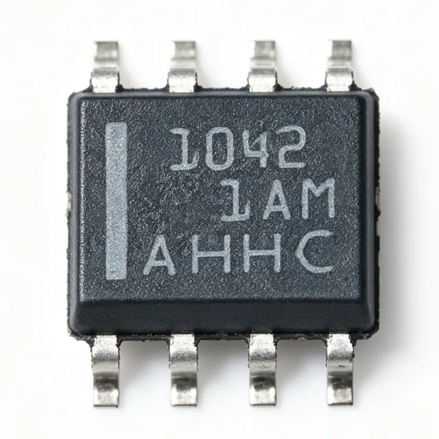
TCAN1042GVDRQ1 - Automotive CAN FD Transceiver | Texas Instruments
TCAN1042GVDRQ1 is an automotive fault-protected CAN transceiver from Texas Instruments, supporting CAN FD data rates up to 5 Mbps with I/O level shifting. It is housed in an 8-pin SOIC (D) package and operates across a temperature range of -55°C to 125°C. A CAN transceiver is a physical layer interface between a CAN controller and the CAN bus twisted-pair wiring. It converts the differential CAN bus signals (CANH/CANL) into single-ended logic levels for the controller, and vice versa. In automotive and industrial networks, the transceiver must handle harsh electrical environments, including voltage transients, ground offsets, and short-circuit conditions, all of which TCAN1042GVDRQ1 is designed to protect against. Key features include fault protection against bus short-circuits and high-voltage transients, I/O level shifting for interfacing with 3.3V or 5V controllers, flexible data-rate operation up to 5 Mbps, and low-power standby mode. The device meets the requirements of ISO 11898-2 for automotive CAN, providing robust communication with a 1/1 driver/receiver configuration and half-duplex operation. Technically, TCAN1042GVDRQ1 integrates a differential driver and receiver, providing differential transmit and receive capability. The I/O level shifting feature allows direct connection to microcontrollers with lower logic levels, eliminating the need for external level translators. Fault protection safeguards the device and bus against short circuits, thermal stress, and voltage surges, ensuring reliable communication in noisy environments. Typical applications include automotive body control modules, gateways, battery management systems, industrial automation, and medical devices where reliable CAN communication is required. The wide operating temperature range and AEC-Q100 qualification (implied by automotive designation) make it suitable for under-hood and harsh environment deployments. During design, ensure proper decoupling capacitors (100 nF and 10 uF) are placed close to the VCC pin to minimize noise, and use the appropriate bus termination resistors (120 ohms) at both ends of the bus. The SOIC-8 package allows compact PCB layouts, but thermal management should be considered for high-temperature environments.

TCAN1042HD - 2 Mbps Fault-Protected CAN FD | Texas Instruments
Texas Instruments TCAN1042HD is a fault-protected CAN transceiver with flexible data-rate support, one CAN transmitter, and one CAN receiver in an 8-pin SOIC package. It supports classic CAN and 2 Mbps CAN FD, operates from a 4.5 V to 5.5 V supply, and is rated for an ambient temperature range of -55°C to +125°C. The device is intended for automotive and industrial networks requiring robust bus fault handling. A CAN transceiver is the physical-layer interface between a CAN controller and a differential CAN bus. It converts logic-level TXD and RXD signals into CAN bus levels and back again. Within the hierarchy of automotive communication ICs, a CAN transceiver is a network interface transceiver, a bus-interface IC, and ultimately a semiconductor. Fault protection adds the ability to survive specified bus faults without permanent damage. The TCAN1042HD provides classic CAN operation together with CAN FD support up to 2 Mbps. Its single-driver, single-receiver organization is suitable for a conventional CAN node rather than a multi-node bus interface. The 4.5 V to 5.5 V supply range supports regulated 5 V systems, while the -55°C to +125°C rating covers demanding automotive temperature ranges. Its 8-pin SOIC package supports conventional surface-mount assembly. The transceiver provides a defined interface between a CAN controller and the differential CANH and CANL conductors. The TXD input accepts controller-generated logic, while RXD presents a logic-level receive signal to the controller. Fault-protected operation is important when the bus may be exposed to short circuits, abnormal voltage conditions, or other faults. ISO 11898-2:2016 physical-layer compliance is specifically identified for this device family. Typical uses include automotive body and powertrain electronics, industrial automation controllers, robotics, building automation, and embedded CAN gateways. A controller such as a CAN FD-capable microcontroller can use the TCAN1042HD for the physical network connection, while external bus protection and filtering may be added where the cable length, topology, or electromagnetic environment requires it. PCB design should keep the CANH and CANL route as a closely coupled differential pair and minimize the area between their return paths. Place transceiver and termination components near the connector or bus-entry point, observe the manufacturer’s grounding and supply-decoupling recommendations, and verify that the controller interface voltage levels match the transceiver logic requirements. This product page combines the device specifications, package and lifecycle information, sourcing workflow, same-family drop-in alternatives, and practical CAN-interface design guidance. It is intended to help engineers identify the correct device and plan a robust PCB implementation without relying solely on a basic distributor listing.
TCAN1044DRQ1 - 8Mbps CAN FD Transceiver, 8-SOIC | Texas Instruments
The Texas Instruments TCAN1044DRQ1 is an automotive-qualified, high-speed Controller Area Network (CAN) transceiver meeting the physical-layer requirements of the ISO 11898-2:2016 standard. It supports both classical CAN and CAN FD (Flexible Data-Rate) networks at data rates up to 8 megabits per second (Mbps), and ships in an 8-pin SOIC (DRB) package with an operating temperature range of -40 C to +125 C. A CAN transceiver is a physical-layer interface IC that bridges a digital CAN protocol controller (typically embedded in a microcontroller) to a differential two-wire CAN bus. The transceiver translates the controller's single-ended TXD/RXD logic signals to the bus's dominant/recessive differential signaling required by ISO 11898-2, while providing bus-side ESD protection, common-mode range, and dominant-time-out fault protection. The TCAN1044-Q1 family sits in the CAN interface IC -> interface IC -> integrated circuit hierarchy and is a foundational building block for in-vehicle networks (IVN). Key features include 8 Mbps CAN FD data-rate support for next-generation vehicle networks, IEC 61000-4-2 ESD protection on bus pins, low-loop delay for propagation-tight networks, and a low-power standby mode with a remote-wake-up wake request via the bus (per the TCAN1044 family datasheet). The device operates from a single 4.5 V to 5.5 V VCC supply, draws typically 50 mA in normal mode, and integrates thermal shutdown plus bus-dominant time-out to prevent network lockup. The TCAN1044DRQ1 architecture uses a high-speed differential driver and a wide-common-mode receiver that exceeds the -2 V to +7 V common-mode range required by ISO 11898-2:2016. Internal level shifting on TXD/RXD allows direct connection to 3.3 V or 5 V microcontrollers without external logic-level translators, and the integrated bus fault protection tolerates -58 V to +58 V transients common in automotive 12 V/24 V systems. Typical applications include automotive body and chassis CAN nodes (BCM, gateway modules), CAN FD powertrain networks, industrial CAN-bus field-bus nodes, and electric-vehicle battery management system (BMS) master/slave communication. The AEC-Q100 Grade 1 qualification makes it appropriate for under-hood and safety-critical vehicle ECUs. When designing with this part, observe the 60 ohm bus termination requirement of ISO 11898-2 and place a 100 nF VCC decoupling capacitor within 2 mm of the supply pin. Avoid routing the CANH/CANL differential pair over splits in reference planes, and use a 120 ohm characteristic-impedance cable/trace geometry. This page synthesizes distributor pricing, drop-in pin-compatible alternatives, and practical PCB design notes for the TCAN1044DRQ1 - information not consolidated in the manufacturer datasheet alone.

TCAN1051-Q1 - Automotive Fault-Protected CAN FD Transceiver | Texas Instruments
TCAN1051-Q1 from Texas Instruments is an automotive fault-protected CAN transceiver with flexible data-rate and sleep mode, meeting ISO 11898-2 (2016) High-Speed CAN physical layer standard. It comes in an 8-pin SOIC package, supporting data rates up to 2 Mbps in CAN FD networks; variants with the G suffix support up to 5 Mbps, while V-suffix versions add a secondary power supply input for I/O voltage. A CAN transceiver is the physical-layer interface between a CAN protocol controller (MCU) and the two-wire differential CAN bus. In the automotive hierarchy, the CAN bus connects ECUs such as engine control, body control, and infotainment modules. The transceiver converts TXD/RXD logic signals from the MCU into differential CANH/CANL signals on the bus and provides bus fault protection. Key features include high on-chip IEC ESD protection, silent mode for reduced power consumption, and AEC-Q100 automotive qualification. The device is designed for harsh automotive environments, with fault protection that withstands bus transients. The flexible data-rate option enables CAN FD networks up to 5 Mbps, making it suitable for modern vehicle architectures that require higher bandwidth. The TCAN1051 family uses a robust physical-layer design with protection diodes and a dominant time-out function, ensuring reliability under bus shorts and high-voltage transients. The device supports both 5 V and (in V variants) 3.3 V I/O reference voltage, allowing direct interface with low-voltage microcontrollers. Typical applications include automotive body control modules, battery management systems, powertrain control, and industrial automation networks. The TCAN1051-Q1 is also widely used in diagnostics (OBD-II) and infotainment systems. Design consideration: ensure proper termination (120 ohm) and place TVS diodes and bus filtering capacitors close to the on-board connectors to prevent transient events from propagating into the PCB.
TCAN1051DRBRQ1 - Automotive CAN FD Transceiver | TI
The Texas Instruments TCAN1051DRBRQ1 is an automotive fault-protected CAN transceiver with CAN FD flexible data-rate support up to 2 Mbps, integrated sleep mode, and a 5 V supply, housed in an 8-pin VSON (DRB) 3x3 mm package rated from -55C to +125C. A CAN (Controller Area Network) transceiver is the physical-layer interface IC that converts the logic-level TXD and RXD signals of a CAN controller into the differential CANH and CANL bus signals defined by ISO 11898. Within the vehicle networking hierarchy, the transceiver sits between the MCU/CAN controller and the twisted-pair bus, providing dominant/recessive signaling, bus fault protection, and low-power standby or sleep behavior for networked electronic control units. Key features include automotive AEC-Q100 qualification, fault protection on the CAN bus pins (protection against faults to battery, ground, and overvoltage per the TI TCAN1051-Q1 product page), CAN FD flexible data-rate support up to 2 Mbps, and a sleep mode that reduces quiescent current for always-on vehicle networks. The -55C to +125C operating range supports under-hood and chassis deployments. The device implements a half-duplex differential physical layer with integrated receiver and driver stages. Internal protection circuitry clamps bus-pin transients and survives DC fault conditions on CANH and CANL, reducing the need for extensive external TVS components in harsh 12 V and 24 V vehicle power environments. Typical applications include body control modules, gateways, ADAS sensor clusters, battery management systems, and industrial CAN networks requiring robust fault tolerance and low standby power. Design consideration: confirm the sleep-mode wake behavior and bus biasing scheme against the TI datasheet, and verify that the 3x3 mm VSON thermal pad is well soldered to ground for transient robustness. This page synthesizes verified distributor listings, drop-in same-family alternatives, and design guidance not consolidated in the manufacturer datasheet.
TCAN1051HD - 2Mbps Fault-Protected CAN FD Transceiver | Texas Instruments
Texas Instruments TCAN1051HD is a fault-protected CAN FD transceiver with flexible data-rate support, operating at up to 2 Mbps and meeting the ISO 11898-2:2016 and ISO 11898-5:2007 physical-layer standards. The device is packaged in an 8-pin SOIC for surface-mount PCB assembly. It supports classic CAN and CAN FD communication, making it suitable for industrial controllers, vehicle electronics, robotics, and embedded systems where fault-tolerant bus interfacing is required. A CAN transceiver is the physical-layer interface between a CAN controller and a CAN bus. It converts controller logic-level TXD and RXD signals into differential CANH and CANL bus levels, while providing receiver filtering, bus-fault protection, and a sleep or standby interface. The TCAN1051HD belongs to the broader CAN interface IC hierarchy, which connects digital controllers and microcontrollers to a robust differential communications network. Fault protection is the primary system-level feature of the TCAN1051HD. According to the Texas Instruments TCAN1051H data sheet, the device is designed for CAN FD networks operating up to 2 Mbps and can withstand bus-fault conditions that occur during wiring errors, short circuits, or induced transients. The operating-temperature range is -55°C to +125°C, supporting demanding industrial and automotive-grade operating environments when the appropriate ordering variant and qualification are selected. The device includes a half-duplex CAN communication path, fault-protected bus interfaces, dominant and recessive receiver outputs, and low-power sleep functionality. It meets ISO 11898-2:2016 for high-speed CAN and ISO 11898-5:2007 for CAN FD physical-layer behavior. These standards define the physical signaling, timing, and fault-handling expectations used by compatible CAN controllers and network equipment. Typical applications include industrial automation controllers, electric-vehicle and vehicle-control modules, robot communication networks, building automation gateways, diagnostic interfaces, and embedded industrial computers. In each case, the transceiver sits between a CAN controller and the differential bus while isolating the controller from the physical CANH and CANL network. Bus termination, common-mode filtering, protection components, and decoupling must be implemented according to the manufacturer data sheet. For PCB design, place the transceiver close to the connector or bus interface to minimize trace area on CANH and CANL. Use a symmetrical pair routing, controlled return-current paths, and the recommended power and ground decoupling. Keep sensitive logic and analog circuitry away from high-energy bus connections, and verify the selected transceiver's sleep-state, enable, and logic-level behavior against the host controller. This product page combines device specifications, standards coverage, engineering application guidance, and drop-in replacement analysis. It is intended to support component selection, PCB planning, and qualification decisions without substituting a new footprint or changing the installed eight-pin SOIC land pattern.