מוצרים (20,000+)

R5F51115ADLF#UA - 32-bit RX111 MCU 128KB Flash USB | Renesas
R5F51115ADLF#UA

R5F51115ADLF#UA - 32-bit RX111 MCU 128KB Flash USB | Renesas

The Renesas R5F51115ADLF#UA is a 32-bit RX111 microcontroller from the RXv1 CPU family, operating at 32 MHz with up to 50 DMIPS and 128 KB (128K x 8) of on-chip Flash memory, 16 KB SRAM, and integrated USB 2.0 Full-Speed device/host/OTG. Housed in a 64-pin FLGA (5x5 mm) surface-mount package, it is part of the Small-capacity ROM / Low Pin Count Lineup of the RX111 Group, designed for ultra-low-power connected applications. What is an RX111 microcontroller? The RX111 Group is Renesas' low-power 32-bit MCU family built on the RXv1 core, an evolution of the RX architecture that combines deterministic real-time response with sub-microamp standby current. The RX111 sits in the broader hierarchy RX sub-family -> 32-bit RISC microcontroller -> embedded MCU -> semiconductor. It targets battery-powered IoT endpoints and USB-connected peripherals where both processing headroom and deep-sleep efficiency are required, with Cortex-M-class competitors positioned on the power-vs-cost boundary. Key features of the R5F51115ADLF#UA include 128 KB Flash with code-flash protection, 16 KB SRAM, 8 KB data flash (work flash), 12-bit A/D converter with up to 14 channels, a 12-bit D/A converter, multiple low-power modes (Sleep, Deep Sleep, Software Standby), a DMA controller (DTMD), and a wide peripheral set including SCI, RSPI, and USB 2.0 FS. Operating from 1.8 V to 3.6 V across -40 C to +85 C (consumer D-version), it draws microamp-level current in software-standby with RTC running. Architecturally the RXv1 core is a Harvard-style 32-bit CISC/RISC hybrid with single-cycle multiply, hardware divider, and a tightly-coupled interrupt controller achieving 50 DMIPS / 1.25 CoreMark per MHz. Renesas' peripheral IP is reused across the RX family for software portability, while the integrated USB 2.0 FS PHY eliminates the external transceiver cost required by many competing Cortex-M0+ designs. Typical applications include USB peripherals (HID, CDC/ACM, Mass Storage), low-power IoT sensor nodes, consumer health devices, smart-home hubs with USB debug ports, industrial bar-code scanners, and battery-powered measurement instruments. The 14-channel 12-bit ADC plus USB makes the R5F51115ADLF#UA particularly attractive for compact instruments that stream analog samples to a host over USB while running for months on a single CR-series coin cell. When designing with this part, engineers should note that the FLGA-64 package does not expose pins on a standard 0.5 mm-pitch hand-solderable outline; reflow assembly with a stencil is mandatory, and the package exposes a central thermal pad that should be soldered for mechanical reliability. Firmware development uses the Renesas e2 studio IDE with GCC-RX or the CC-RX compiler. This page synthesizes distributor stock and pricing, RX111 same-family and cross-vendor drop-in alternatives, USB firmware considerations, and practical design notes for low-power USB peripherals not found on a single manufacturer datasheet. Availability is confirmed across DigiKey, Mouser, LCSC, and Octopart as of 2026-10-10.

RFQ צור קשר
R5F51308ADFN#30 - RX130 32-bit 32MHz MCU 512KB Flash | Renesas
R5F51308ADFN#30

R5F51308ADFN#30 - RX130 32-bit 32MHz MCU 512KB Flash | Renesas

The Renesas R5F51308ADFN#30 is a cost-optimized, high-performance 32-bit RX130 microcontroller built around the RXv1 CPU core, delivering 50 DMIPS at 32 MHz and integrating 512 KB of flash memory plus 48 KB of SRAM. The device is housed in an 80-pin LFQFP (12x12 mm) package and operates from a single 1.8 V to 5.5 V supply, supporting both battery-powered and 5 V industrial rails. A microcontroller (MCU) is a single-chip computer that integrates a CPU core, non-volatile program memory (flash), volatile working memory (RAM), and a wide range of peripheral interfaces such as ADC, timers, communication controllers, and capacitive-touch hardware. The RX130 sits inside the broader Renesas RX family (RX100/RX200/RX600/RX700) and is positioned as the cost-optimized, ultra-low-power entry tier with on-chip touch sensing. LDOs, op-amps, and reset supervisors are typically placed around the RX130 to build a complete power-tree for human-machine interface (HMI), home appliance, and industrial-sensor designs. Key features include up to 36 channels of capacitive touch sensing with improved noise immunity, sensitivity, and water resistance versus previous RX touch generation, a 12-bit A/D converter, a D/A converter, a real-time clock (RTC), IEC60730 compliance for appliance-safety code libraries, and up to 6 communication channels. The wide 1.8 V to 5.5 V supply range allows direct connection to 5 V sensors and human-machine interface panels without level shifters. An integrated RTC and low-power modes make standby power budgets achievable for battery-operated appliances. The RXv1 core is paired with single-precision FPU hardware support and tightly-coupled flash that supports zero-wait-state execution at 32 MHz, giving 50 DMIPS performance suitable for user-interface controllers, sensor fusion, and small protocol stacks. The capacitive-touch peripheral runs autonomously from the CPU, leaving the core free for application logic and reducing interrupt load in noisy environments. Hardware IEC60730 class-B support accelerates functional-safety certification for white goods. Typical applications include home appliance user interfaces with touch keys, industrial control panels, battery-powered sensor nodes, building automation keypads, and small motor-control boards that need ADC plus timer resources on a single 5 V rail. The 80-pin LFQFP exposes ample GPIO for parallel displays, button matrices, and brushless-DC FET drivers. When designing with the RX130, place the decoupling network as close as possible to the power pins, route touch-sensing traces with guard rings, and confirm IEC60730 firmware libraries are linked when targeting white-goods safety standards. Always validate the touch-sensing threshold with the production PCB stack-up. This page synthesizes distributor pricing, drop-in alternative analysis, and practical design notes not consolidated in the Renesas datasheet alone.

RFQ צור קשר
R5F51308ADFP#30 - RX130 32MHz 512KB Flash MCU | Renesas
R5F51308ADFP#30

R5F51308ADFP#30 - RX130 32MHz 512KB Flash MCU | Renesas

The Renesas Electronics R5F51308ADFP#30 is a 32-bit RX130 microcontroller running at 32 MHz with 512 KB Flash and 48 KB SRAM, housed in a 100-pin LFQFP (14x14 mm) package. It is part of the RX130 family - a cost-optimized, high-performance 32-bit MCU group with enhanced capacitive touch key function and 5 V operation support, delivering up to 50 DMIPS per the verified distributor listings. A microcontroller (MCU) is a single-chip computer containing a CPU core, program memory (Flash), data memory (SRAM), and on-chip peripherals such as timers, communication interfaces, ADCs, and touch sensing. MCUs form the lowest tier of the embedded computing hierarchy: embedded processor -> microcontroller -> 32-bit MCU -> RX130 family. They sit beneath microprocessors (MPUs) in capability but above discrete logic in integration, enabling compact, low-power designs for appliance, industrial, and human-machine-interface (HMI) products. Key features of the R5F51308ADFP#30 include 88 I/O pins (per JLCPCB listing), a 12-bit A/D converter with up to 36 capacitive touch sensing channels, an 8-bit D/A converter, 6 communication channels (including SCI, I2C, and SPI variants), an RTC, IEC60730 compliance support for household appliance safety standards, and a wide 1.8 V to 5.5 V single-supply operating range. The device uses the proprietary RXv1 CPU core with single-precision FPU. The RX130 architecture combines deterministic interrupt response with low-power operation, making it well suited for white goods, sensor HMI, and battery-friendly IoT edge nodes. The integrated touch sensing unit uses an improved mutual-capacitance detection method providing better noise immunity, sensitivity, and water resistance versus earlier Renesas touch MCUs. Typical applications include washing machine and refrigerator control boards, induction cooktop user interfaces, smart thermostat keypads, industrial sensor HMI panels, and small IoT sensor hubs. The wide 5 V tolerance simplifies interfacing with legacy analog front-ends and white-goods actuator drivers. When designing with this part, remember that the R5F51308ADFP#30 is the 100-pin / 512 KB / -40C to +85C industrial-grade variant. For lower pin counts, smaller flash, or extended temperature (-40C to +105C) refer to other RX130 group members listed in the family datasheet (R01DS0243EU0300). This page synthesizes distributor pricing, drop-in same-package alternatives, and practical design notes not found in the manufacturer datasheet, with cross-references verified against the Renesas RX130 group datasheet and authorized distributor data as of 2026-10-10.

RFQ צור קשר
R5F52203BDFL - 32MHz 32-bit RX220 MCU, 64KB Flash, LQFP-48 | Renesas
R5F52203BDFL

R5F52203BDFL - 32MHz 32-bit RX220 MCU, 64KB Flash, LQFP-48 | Renesas

The Renesas Electronics R5F52203BDFL is a 32-bit RX220 family microcontroller built on the RXv1 core, delivering 32 MHz CPU performance with 64 KB of on-chip flash and 8 KB of SRAM in a 48-pin LFQFP (7x7 mm) package. It is an entry-level RX200 MCU positioned for designs needing minimum peripheral count, low active power, and small footprint. An entry-level 32-bit MCU (microcontroller unit) integrates a CPU core, on-chip flash program memory, SRAM, and a curated set of peripherals into a single IC. Within the broader hierarchy it sits between 8/16-bit legacy MCUs and high-performance Cortex-M/RX700 parts. The RX220 series in particular is the slimmed-down, low-pin-count derivative of the RX210 family, retaining pin-compatibility and the same RXv1 instruction set while trimming unused peripherals to reduce cost and active current. Key features include 64 KB (64K x 8) flash, 8 KB SRAM, up to 32 MHz CPU clock, a 12-bit A/D converter, multi-function timer (MTU2), and serial interfaces (SCI, I2C-bus compatible, RSPI). Supply voltage spans 1.8 V to 5.5 V, supporting both 3.3 V and 5 V system rails. The device also integrates watchdog timer, real-time clock, low-voltage detection, and on-chip debugging via a single-wire interface. Architecturally, the RX220 uses a 3-stage pipelined RXv1 core with hardware MAC (multiply-accumulate) instructions, supporting C-level DSP routines without an extra DSP unit. The 1.8 V internal core regulator and selectable low-power modes (Sleep, Deep Sleep) reduce quiescent current to a few microamps, enabling coin-cell powered designs. Typical applications include consumer appliances, sensor signal conditioning, battery-driven IoT nodes, low-end motor control, and human-interface boards replacing 8/16-bit MCUs. The wide 1.8-5.5 V supply simplifies migration from 5 V legacy systems. Consider total power budget: at 32 MHz active and 3.3 V, the core draws several mA, so duty-cycling is essential for battery lifetime. This page synthesizes distributor pricing, drop-in alternatives, and design notes not found in the standalone datasheet.

RFQ צור קשר
R5F52205BDFP#10 - 32MHz RX220 MCU 128KB Flash 100-LFQFP | Renesas
R5F52205BDFP#10

R5F52205BDFP#10 - 32MHz RX220 MCU 128KB Flash 100-LFQFP | Renesas

The Renesas Electronics R5F52205BDFP#10 is an entry-level 32-bit RX220 microcontroller featuring a 32MHz RXv1 core, 128KB flash, and 8KB SRAM, housed in a 100-pin LFQFP (14x14mm) package. It is part of the RX220 Group, a slimmed-down derivative of the RX210 family with high pin-arrangement and software compatibility. Operating from 1.62V to 5.5V, this MCU targets cost-sensitive applications requiring minimum peripheral count and low power consumption. What is a microcontroller (MCU)? A microcontroller is a single-chip computer that integrates a CPU core, program memory (flash), data memory (SRAM), and peripherals such as timers, communication interfaces, and analog blocks. The RX220 family sits within the broader taxonomy: 32-bit MCU -> microcontroller -> embedded processor -> semiconductor IC. RXv1 cores use the Renesas RX instruction set, delivering high code density and deterministic interrupt response suited to real-time embedded designs. Key features of the R5F52205BDFP#10 include 128KB flash with 8KB SRAM, a 32MHz maximum operating frequency, and an industrial temperature grade of -40C to +85C. The device integrates a minimum set of peripherals aimed at entry-level designs: multiple timers, a 12-bit A/D converter, and serial communication interfaces. The 100-pin LFQFP package provides ample I/O for typical embedded applications while remaining cost-effective for high-volume production. The RX220 Group achieves high pin-arrangement and software compatibility with the higher-end RX210 Group, allowing engineers to migrate designs upward as memory or peripheral needs grow. This compatibility reduces design risk and accelerates time-to-market when scaling from entry-level to mid-range applications. Typical applications include home appliances, consumer electronics, industrial sensor nodes, simple motor control, and battery-powered measurement instruments. The wide 1.62V-5.5V operating range supports both 3.3V and 5V system designs without external level translation. When designing with this MCU, ensure the power supply rail stays within 1.62V-5.5V during all transient conditions, and follow Renesas RX220 hardware manual guidance for oscillator and reset circuit design. Unused pins should be configured with appropriate input pull-ups or left open per the hardware manual to minimize power consumption. This page synthesizes distributor pricing from DigiKey, Mouser, and LCSC, drop-in alternatives from the RX220 family and cross-brand ARM Cortex-M0+ competitors, and practical design notes not consolidated in the manufacturer datasheet.

RFQ צור קשר
R5F52206BDFP#V0 - 32-bit RX220 MCU 256KB Flash LFQFP-100 | Renesas
R5F52206BDFP#V0

R5F52206BDFP#V0 - 32-bit RX220 MCU 256KB Flash LFQFP-100 | Renesas

The Renesas R5F52206BDFP#V0 is an entry-level 32-bit RX220 microcontroller built on the RXv1 CPU core, delivering 32 MHz CPU speed with 256 KB flash memory and 16 KB SRAM in a 100-pin LFQFP (14x14 mm) package. It operates across 2.7 V to 5.5 V supply ranges and supports industrial temperature grades, making it suitable for cost-sensitive embedded designs that need more performance than 8-bit MCUs but minimal BOM complexity. What is a 32-bit microcontroller (MCU)? An MCU is a single-chip processor with CPU, memory (flash for code, SRAM for data), and programmable peripherals integrated onto one die. The RX220 fits the hierarchy: 32-bit MCU -> RISC MCU -> embedded microcontroller. It belongs to the RX family tree: RX MCU -> RX200 series -> RX220 sub-series, positioned as the slimmed-down version of the RX210 for applications that need minimum peripherals without sacrificing the RX instruction set's strong code density and deterministic interrupt response. Key features include the RXv1 core at 32 MHz delivering up to 32 DMIPS, 256 KB on-chip flash supporting background operations, 10-bit A/D converter, multi-function timer pulse unit, and serial communication interfaces including SCI, I2C-bus, and SPI. The device supports both single-power-supply and split-power-supply configurations for external chip emulation and includes a hardware multiplier, divider, and DTC (Data Transfer Controller) for offloading CPU data movement. Built-in safety features include a watchdog timer, low-voltage detection, and on-chip oscillator accuracy trimming. Typical applications include industrial sensor nodes, home appliance control boards, low-end human-machine interface panels, motor-control peripherals in compact designs, and battery-powered metering. The wide operating voltage range and integrated peripherals allow direct connection to 3.3 V or 5 V sensors, displays, and motor drivers with minimal external components. The LFQFP-100 package provides a generous 1.0 mm lead pitch for cost-effective two-layer PCB assembly. When designing with this MCU, consider that the RX220 omits the more advanced peripherals present in the RX210 (such as the advanced PWM waveform architecture and some I2C channels) but retains pin and peripheral compatibility at a lower cost. Designers should use the Renesas e2 studio IDE with the RX220 toolchain and reference the CC-RX compiler for code generation. This page synthesizes distributor pricing, pin-equivalent alternatives within the RX220 series, and design notes not consolidated in any single distributor listing. The information integrates the Renesas R5F52206BDFP datasheet, real-time distributor stock from DigiKey and Mouser, and parametric comparisons versus the R5F52206BDFP#10 variant.

RFQ צור קשר
R5F52306ADFM#30 - RXv2 32-bit MCU 256KB Flash | Renesas
R5F52306ADFM#30

R5F52306ADFM#30 - RXv2 32-bit MCU 256KB Flash | Renesas

The Renesas Electronics R5F52306ADFM#30 is a 32-bit RXv2-core microcontroller from the RX230 family, operating at up to 54 MHz and delivering 88.56 DMIPS while integrating a single-precision FPU for DSP-class math in power-constrained applications. The device combines 256 KB of code flash and 32 KB of SRAM on-chip, packaged in a 64-pin LFQFP (10x10 mm) form factor. This part variant uses the #30 Renesas ordering code suffix that designates the operating temperature grade and shipping form. A microcontroller (MCU) is an integrated circuit that combines a CPU core, program and data memory, and a set of peripherals in a single chip. The RX family belongs to the broader category of 32-bit embedded microcontrollers in the power management and embedded computing domain, positioned between 16-bit MCUs (such as the PIC24 or RL78 families) and 64-bit application processors. The RXv2 core supersedes the original RX core with enhanced DSP and FPU throughput, and the RX230 sub-family emphasizes ultra-low power consumption alongside USB 2.0 Full-Speed host/function/OTG, CAN, SD host interface, serial sound interface, and a capacitive touch sensing unit. Key features of the R5F52306ADFM#30 include 256 KB flash (256K x 8), 32 KB SRAM, integrated capacitive touch sensing, hardware AES and TRNG security options, and a rich peripheral set spanning multiple SCI, I2C, SPI, RSPI, and CAN channels. The RXv2 core implements Harvard cache, single-cycle MAC, and a single-precision FPU, allowing efficient digital signal processing without an external DSP. Low-power modes include deep standby and several software-controlled sleep states that draw microamps, enabling coin-cell or energy-harvest powered designs. In terms of architecture, the RX230 is implemented in a 40 nm-class low-leakage CMOS process and pairs the RXv2 core with dedicated low-power peripherals and an interrupt controller (ICU) supporting NMI and 16 priority levels. The chip supports JTAG and FINE debug interfaces for in-circuit emulation, and the flash memory is programmable via the onboard SCI bootloader. Typical applications for the R5F52306ADFM#30 include human-machine interface (HMI) panels with capacitive touch, low-power IoT sensor nodes, USB peripherals (HID, CDC, vendor classes), battery-powered industrial sensors, building automation controllers, and small motor control subsystems. The integrated touch sensing unit and USB 2.0 FS OTG make it especially well suited for connected appliances, white goods, and consumer electronics. When designing with the RX230, allow sufficient decoupling (100 nF + bulk) on each VCC/VSS pair and follow the Renesas RX230 hardware manual layout for the analog AVCC rail when using the ADC. Take care to respect the flash programming voltage ramp timing and the recommended thermal profile (peak 260 C) during reflow to avoid internal flash stress. This page synthesizes distributor pricing, same-family Renesas drop-in alternatives, and application guidance beyond what is included in the manufacturer's datasheet, helping engineers shorten the BOM selection cycle.

RFQ צור קשר
R5F52316ADFP#10 - 54MHz RX231 256KB Flash MCU | Renesas
R5F52316ADFP#10

R5F52316ADFP#10 - 54MHz RX231 256KB Flash MCU | Renesas

The Renesas R5F52316ADFP#10 is a 32-bit RX231 microcontroller built on the RXv2 core with integrated single-precision FPU and enhanced DSP, delivering 88.56 DMIPS at 54 MHz maximum operating frequency. The device integrates 256 KB of flash memory and 32 KB of SRAM, and is housed in a 100-pin LFQFP package measuring 14x14 mm. It supports USB 2.0 full-speed host/function/OTG, CAN, SD host interface, serial sound interface, and a capacitive touch sensing unit, making it a flexible mixed-signal MCU for human-machine-interface and connected embedded designs. What is a low-power high-performance RX MCU? The RX231 belongs to Renesas' RX200 family of low-power 32-bit microcontrollers based on the RXv2 architecture, which combines an enhanced Harvard bus with a hardware FPU and DSP extensions. Within the broader taxonomy, R5F52316ADFP#10 is a microcontroller (MCU) -> embedded processor -> semiconductor, positioned for energy-conscious applications that still require DSP-class math and rich connectivity. Key features include a wide operating voltage range from 1.8 V to 5.5 V, integrated 12-bit A/D converter with up to 4 channels of D/A, real-time clock, and security functions such as a unique hardware ID and AES-style acceleration. It also integrates a capacitive touch sensing unit (CTSU) that simplifies implementing waterproof touch buttons and sliders without external components. Multiple low-power modes - including deep software standby drawing only a few microamps - extend battery life across portable and always-on use cases. From an architectural standpoint, the RXv2 core features a 5-stage pipeline, single-cycle MAC, and dedicated FPU, achieving up to 1.65 DMIPS/MHz. The MCU supports up to 70 GPIO pins, multiple serial interfaces (SCI, I2C, SPI, RSPI), and an external bus interface for memory expansion. ECC on flash and SRAM, watchdog timers, and a low-voltage detector add functional-safety features that simplify IEC/UL consumer-safety designs. Typical applications include home appliances with touch UI, IoT sensor nodes, USB peripherals, industrial HMI panels, and low-power connected medical devices. The wide 5.5 V tolerance also makes the device robust in 24 V industrial bus systems after simple LDO regulation. When designing with R5F52316ADFP#10, evaluate the 5 V-tolerant GPIO count and the integrated CTSU to reduce BOM in touch-UI designs. For production programming, Renesas' e2 studio and the Flash Development Toolkit support on-board programming via the SCI bootloader. This page synthesizes distributor pricing, cross-brand pin-compatible alternatives, and design notes not duplicated on the manufacturer product page.

RFQ צור קשר
R5F56216BDFB - 100MHz 32-bit RX621 MCU, 256KB Flash | Renesas
R5F56216BDFB

R5F56216BDFB - 100MHz 32-bit RX621 MCU, 256KB Flash | Renesas

The Renesas R5F56216BDFB is a 32-bit microcontroller from the RX621/RX62N family, operating at up to 100 MHz with 165 DMIPS core performance and delivering up to 512 Kbytes of on-chip Flash memory in a 144-pin LFQFP (20x20 mm) package. The device integrates 256 KB Flash, 64 KB SRAM, USB 2.0 Host/Function, CAN, and peripheral functions targeted at industrial and consumer connectivity. An RX-family microcontroller is a 32-bit RISC MCU built around the Renesas RXv1 core, sitting in the hierarchy above 8/16-bit microcontrollers and below general-purpose DSPs in embedded-system taxonomy. The RX core combines single-cycle execution, an on-chip FPU, and tightly-coupled memory architecture to deliver deterministic real-time performance while retaining C-language programming ease. This category is widely used in industrial automation, building controls, and human-machine interface (HMI) equipment where deterministic interrupt latency and rich connectivity are required. Key features of the R5F56216BDFB include 100 MHz maximum operating frequency, 165 DMIPS at 1.25 DMIPS/MHz, hardware multiply/divide and FPU support, 256 KB Flash program memory, 64 KB SRAM, USB 2.0 Host/Function Controller, CAN interface, 10-bit A/D converter, multifunction timer (MTU2), DMA controller (DMAC/DTC), and a wide operating voltage range suitable for 3.3 V systems. The 144-pin LFQFP package provides ample I/O for parallel buses and external memory interfaces. Architecturally, the RX621 uses a 5-stage pipeline Harvard architecture with separate instruction and data buses, integrated FPU for IEEE-754 single-precision operations, a dedicated flash access accelerator, and 16 KB of user-accessible data flash. The integrated peripheral bridge supports up to 123 I/O lines along with rich serial channels including SCI (UART/IrDA/I2C), RSPI, and the USB 2.0 Host controller with embedded PHY. Typical applications include industrial serial-to-Ethernet gateways, building automation controllers, USB host devices such as printers and POS terminals, factory automation PLCs, and consumer devices requiring both Ethernet and CAN connectivity. The wide operating voltage and temperature range also suit HVAC and motor-control peripherals. When designing with this part, ensure the USB PHY reference resistor and decoupling follow the datasheet reference design, and that firmware uses the on-chip flash-access accelerator to keep interrupt latency well below 1 us at 100 MHz operation.

RFQ צור קשר
R5F56216BDFB#V0 - 100MHz RX MCU 256KB Flash 144-LFQFP | Renesas
R5F56216BDFB#V0

R5F56216BDFB#V0 - 100MHz RX MCU 256KB Flash 144-LFQFP | Renesas

The Renesas R5F56216BDFB#V0 is a 32-bit RX600-series microcontroller built around the high-performance RX v1 CPU core, delivering 100 MHz operation with single-precision FPU, 165 DMIPS throughput, and 256 KB of on-chip Flash plus 64 KB SRAM in a 144-pin LFQFP (20x20 mm) package. The part integrates connectivity peripherals including Ethernet MAC, USB 2.0 Full-Speed Host/Function, CAN, and multiple serial interfaces, alongside a 12-bit ADC, timers, and a rich-function DTC and DMA engine. Operating voltage is 2.7 V to 3.6 V from a single supply, with multiple low-power modes for energy-aware applications. A 32-bit MCU is a microprocessor in which the data path, registers, and ALU are 32 bits wide, allowing a single instruction to handle larger integer and floating-point values than an 8- or 16-bit controller. The RX core sits in the broader taxonomy as 32-bit microcontroller -> embedded MCU -> semiconductor -> integrated circuit. Combining high CPU throughput, large SRAM, and integrated connectivity, the RX621 family targets applications that previously required an external host processor plus discrete communication ICs. Key features include 100 MHz core with 165 DMIPS, hardware single-precision FPU, 256 KB Flash / 64 KB SRAM, 10 KB data Flash, Ethernet MAC, USB 2.0 FS Host/Function, CAN, and up to 123 I/O pins. The 12-bit ADC achieves up to 1 Msps with three sample-and-hold units, while the EXDMAC and DTC subsystems handle data movement without CPU intervention. Typical applications include industrial Ethernet gateways, factory automation controllers, USB-connected human-machine interfaces (HMIs), building-automation concentrators, and CAN-connected sensor hubs. The wide peripheral mix and large SRAM also make the part suitable for point-of-sale terminals and small-format IoT edge nodes. When designing with the R5F56216BDFB#V0, allocate decoupling per the hardware manual, observe the 0.5 mm LQFP pitch soldering profile (JEDEC J-STD-020 MSL classification applies), and verify the pin assignments against the device's full 144-pin LQFP variant symbol. The part is RoHS-compliant per Renesas product information. This page synthesizes distributor pricing, drop-in same-package alternatives from the RX621 family, and practical design notes that complement the official Renesas hardware manual rather than repeating it verbatim.

RFQ צור קשר
R5F56218BNFP - 100MHz 32-bit RX MCU | Renesas
R5F56218BNFP

R5F56218BNFP - 100MHz 32-bit RX MCU | Renesas

Renesas Electronics R5F56218BNFP is a 32-bit RX-series microcontroller with a floating-point processing unit, a maximum clock frequency of 100 MHz, and performance of up to 165 DMIPS. The device includes 512 KB of flash memory and is supplied in a 100-lead LQFP package. Its square gull-wing package provides 100 externally accessible connection points and is intended for designs requiring substantial mixed-signal, communications, and control integration. A microcontroller is a semiconductor device that executes embedded software from internal program memory while controlling sensors, communications interfaces, actuators, and other system hardware. In the product hierarchy, this R5F56218BNFP is a 32-bit MCU, a type of embedded processor used above simple logic controllers and below more complex application processors. Its RX-series positioning combines high-frequency execution with integrated real-time control capabilities for industrial equipment and embedded systems. Verified source data identifies a 100 MHz operating frequency, 165 DMIPS performance, an FPU, 512 KB flash memory, and 100-pin QFP packaging. The floating-point unit accelerates arithmetic used in control algorithms, signal processing, and data acquisition, while the 512 KB code and data-memory resource supports larger embedded applications than basic control MCUs. The 100 MHz clock provides additional scheduling headroom for communications protocols and simultaneous peripheral operation. The 100-lead LQFP package offers a high pin count compared with small-outline MCUs, supporting a broader mix of digital I/O and dedicated peripheral connections. This makes the R5F56218BNFP useful where a board requires numerous interface signals, mixed external devices, or several communication functions. Its relatively large gull-wing footprint also provides visible solder joints and is generally compatible with conventional reflow and inspection processes, although it requires more PCB area than a compact QFN or leadless package. Typical application directions include industrial automation, factory equipment, motor and motion control, measurement systems, communications equipment, and compact embedded control platforms. The 100 MHz processing rate and FPU support workloads combining protocol handling with real-time calculations. Such systems should still validate interrupt latency, peripheral resource allocation, memory utilization, and analog performance against the complete manufacturer documentation before production release. A critical design consideration is that the supplied search data does not include the complete electrical characteristics or pin map. Before schematic capture, verify supply voltage, I/O limits, clock configuration, peripheral multiplexing, pin states during reset, and exposed thermal or power requirements in the official Renesas datasheet. Because this is a 100-pin device, use a symbol and footprint whose assignments have been checked against the exact NFP ordering code rather than relying only on a generic QFP footprint. This page consolidates verified distributor specifications, package information, availability references, and carefully qualified replacement context for R5F56218BNFP. It also distinguishes confirmed data from parameters that require the manufacturer datasheet, helping engineers identify procurement, compatibility, and design-validation tasks before committing a 100-LQFP board to production.

RFQ צור קשר
R5F562T7DDFP#V1 - 100MHz RX62T MCU 128KB Flash | Renesas
R5F562T7DDFP#V1

R5F562T7DDFP#V1 - 100MHz RX62T MCU 128KB Flash | Renesas

The Renesas R5F562T7DDFP#V1 is a 32-bit RX62T microcontroller built around the high-performance RX600 CPU core, operating at a maximum frequency of 100 MHz and delivering up to 165 DMIPS with an integrated single-precision FPU. It integrates 128 KB of on-chip flash memory, 8 KB of SRAM, and a rich set of motor-control peripherals including the Multi-Function Timer Pulse Unit (MTU3), General PWM Timer (GPT), high-speed 12-bit A/D converter, and 10-bit A/D converter, all housed in a 100-pin LFQFP (14x14 mm) package. A 32-bit microcontroller (MCU) is a programmable processor-on-a-chip that integrates CPU core, non-volatile program memory, working RAM, and a wide variety of analog and digital peripherals onto a single silicon die. Within the broader electronics taxonomy, MCUs sit under microcontrollers -> microprocessors -> embedded processors -> semiconductors, and they are the central computational element in nearly every modern electronic product from washing machines to industrial robots. The RX62T family specifically belongs to the RX600 Series, Renesas's high-performance RX CPU architecture that targets real-time control applications with CISC-style instruction set and deterministic interrupt handling. Key features include 165 DMIPS core performance, hardware FPU for floating-point motor-control math, dual A/D converter subsystems (12-bit high-speed + 10-bit auxiliary), 100-pin LFQFP package, supply voltage of 4.0V to 5.5V, and built-in safety features targeting IEC60730 compliance for home appliances. The integrated MTU3 and GPT timers can drive three-phase PWM outputs directly, eliminating external logic for variable-frequency drives. The RX62T architecture uses a Harvard-style CISC core with 32-bit registers, hardware multiply-accumulate (MAC), and a single-precision IEEE-754 FPU. This combination delivers deterministic execution timing critical for field-oriented control (FOC) loops running at 16 kHz or higher. The 128 KB flash is supported by 8 KB SRAM, providing adequate headroom for sensorless-FOC firmware with observer algorithms. Typical applications include three-phase motor drives (BLDC, PMSM, ACIM), home appliance motor control (washing machines, refrigerators, air conditioners), industrial servo drives, and fans/pumps. The on-chip dual A/D allows simultaneous sampling of phase currents and DC-bus voltage within a few hundred nanoseconds. When designing with this part, allocate the 100-pin LFQFP footprint and use the Renesas e2studio or CS+ toolchain with the RX compiler. Reserve one of the on-chip 12-bit A/D channels for DC-bus sensing and dedicate the GPT/MTU3 channels for inverter PWM generation; this avoids software latency in the current-sense path. This page synthesizes distributor pricing, same-brand drop-in alternatives (R5F562T7DDFP#V0, R5F562T7DDFP#11), and practical motor-control design notes not found in the manufacturer datasheet alone.

RFQ צור קשר
R5F56318CDFP#V0 - RX631 100MHz 512KB Flash MCU | Renesas
R5F56318CDFP#V0

R5F56318CDFP#V0 - RX631 100MHz 512KB Flash MCU | Renesas

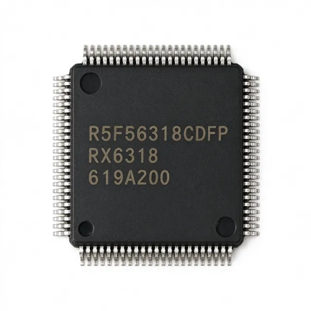
The Renesas R5F56318CDFP#V0 is a 32-bit RX631 microcontroller featuring a 100 MHz RXv1 CPU core, 512KB of flash memory, and 128KB of SRAM, housed in a 100-pin LFQFP package (14x14 mm). The RX631 belongs to the RX600 family and is designed for embedded applications requiring a balance of performance, peripheral integration, and power efficiency. A microcontroller (MCU) is a single-chip computer that integrates a CPU, memory, and programmable peripherals on a single silicon die. MCUs are the heart of embedded systems, ranging from home appliances and industrial controllers to automotive ECUs and IoT edge nodes. The RX family sits in the high-performance 32-bit MCU tier alongside ARM Cortex-M, RISC-V, and proprietary cores, offering deterministic real-time behavior and rich connectivity. Within that hierarchy, the RX631 is an Ethernet-less variant of the RX63N, traded off to enable lower-cost designs that still require the full peripheral set. The R5F56318CDFP#V0 integrates a 12-bit ADC with up to 21 channels, motor-control timers, multiple SCI (UART), RSPI, I2C, and CAN interfaces. It supports 2.5V and 3.3V operation and incorporates safety and security features suitable for industrial and consumer designs. The LFQFP-100 package provides ample I/O for connectivity-rich applications while remaining manageable on a 2-layer PCB with careful layout. Typical applications include industrial motor control, building automation controllers, factory equipment HMI panels, and consumer devices with graphical interfaces. The combination of CAN, multiple serial channels, and ADC performance also makes it suitable for sensor aggregation nodes and small inverter drives. When designing with the R5F56318CDFP#V0, place a 4.7 uF bulk capacitor and 100 nF decoupling capacitor near each VCC pin pair. For CAN communications, add a 120 ohm termination resistor at each bus end. Avoid routing high-speed signals under the MCU to prevent coupling noise into the analog supply. This page synthesizes distributor pricing, drop-in Renesas RX family alternatives, and practical PCB layout guidance not consolidated in the manufacturer datasheet.

USD $16.08 צור קשר
R5F5631BCDFP - 100MHz 32-bit RX MCU, 1MB Flash | Renesas
R5F5631BCDFP

R5F5631BCDFP - 100MHz 32-bit RX MCU, 1MB Flash | Renesas

The Renesas Electronics R5F5631BCDFP is a 100-MHz 32-bit RX RX631/RX63N microcontroller with 1 MB of on-chip flash memory and 128 KB of SRAM, housed in a 100-pin LFQFP package measuring 14 x 14 mm at 0.50 mm pitch. It integrates a single-precision hardware FPU delivering 165 DMIPS of performance and a rich peripheral set including 12-bit ADC, motor-control timers, SCI, RSPI, I2C, CAN, full-speed USB 2.0 host/function/OTG, and an Ethernet MAC. An RX microcontroller (RX MCU) is a 32-bit microcontroller family built by Renesas around the proprietary RXv1 instruction set, designed for deterministic real-time control with hardware floating-point support. RX MCUs sit in the broader taxonomy of microcontrollers -> embedded processors -> 32-bit MCUs -> ARM/RISC-V/RX-class cores -> semiconductor devices, and they specifically target motor control, industrial networking, and graphical HMI workloads where deterministic interrupt latency and rich connectivity matter. Key features include 1 MB on-chip flash (organised as 1 M x 8 in the datasheet) supporting in-system programming, 128 KB SRAM with background ECC, 12-bit A/D converter modules with multiple channels, multi-function timer pulse units supporting complementary PWM for three-phase motor drive, and safety functions such as a register write protection, clock-failure detection, and an independent watchdog timer. Architecturally, the chip uses a 3-stage pipelined RXv1 core with a 32-bit multiplier and single-precision FPU, allowing floating-point DSP tasks (FFT, IIR/FIR filtering, current-loop math) to execute at full core clock. Memory protection, dual-bank flash for live firmware updates, and ELC (event link controller) hardware event routing minimise CPU intervention in motor-control and communication loops. Typical applications include Ethernet-enabled industrial PLCs, building automation controllers, USB-class human interface devices, CAN/J1939 automotive body controllers, and EtherCAT/CANopen slave nodes on RX631 Group. The wide operating voltage range and built-in Ethernet MAC also suit smart energy concentrators. When designing in, plan for external decoupling near each VDD/VSS pair, follow the datasheet's recommended PCB land pattern for the LFQFP-100, and reserve boot-mode pins for the factory firmware programming sequence.

RFQ צור קשר
R5F5631MCDFL#V0 - 100MHz 32-bit RX631 MCU 256KB Flash | Renesas
R5F5631MCDFL#V0

R5F5631MCDFL#V0 - 100MHz 32-bit RX631 MCU 256KB Flash | Renesas

The Renesas R5F5631MCDFL#V0 is a 100 MHz 32-bit RX631 microcontroller built on the RXv1 CPU core, packaged in a 48-pin LFQFP (7x7 mm). It integrates 256 KB of on-chip Flash and 64 KB of SRAM with peripheral IP such as 12-bit ADC, multi-function timer pulses, SCI, RSPI, I2C, CAN, USB 2.0 host/function, and Ethernet MAC. Operating voltage is 2.5V to 3.3V (typical industrial 3.3V). The part is qualified for industrial and consumer embedded control where deterministic 32-bit performance and rich connectivity are required. A 32-bit microcontroller (MCU) is a single-chip computer that integrates a CPU core, program and data memory, and a wide range of on-chip peripherals. The RX631 family sits in the hierarchy RXv1 core -> RX600 family -> RX series -> 32-bit MCU -> embedded microcontroller -> semiconductor, positioning the device between low-end 8/16-bit MCUs and application processors. It excels in deterministic real-time control with single-cycle multiply-accumulate, hardware FPU optional, and built-in safety features such as memory protection, register write protection, and an on-chip watchdog. Differentiating features of R5F5631MCDFL#V0 include 100 MHz core speed delivering 235 DMIPS, on-chip 4 KB data Flash for EEPROM emulation, dual 12-bit ADC units up to 1 MSPS each, 16-bit timer pulse units supporting motor-control PWM, up to 14 communication interfaces including CAN (1 channel), USB 2.0 host/function, Ethernet MAC, I2C, RSPI, and SCI. The block diagram emphasizes energy-efficient operation with low-power run/standby modes, RTC with calendar, and a temperature sensor interface. Direct-memory-access controllers (DMAC/DTC) reduce CPU overhead for data movement between peripherals and memory. Technically, the RXv1 core is a 5-stage pipelined RISC architecture with Harvard-style bus structure and hardware integer multiplier/divider, providing high code density and predictable interrupt latency. The on-chip Flash uses single-cycle flash-IO for wait-state-free 100 MHz fetch. Analog integration includes 8x 12-bit ADC inputs at 1 MSPS, two 10-bit DAC channels, and a comparator that supports motor-control feedback loops. The safety suite contains IEC 60730 Class B support with hardware CRC, ILLEGAL address detection, and a register-write-protect function for safety-critical firmware integrity. Typical applications for R5F5631MCDFL#V0 include industrial motor-control inverters, factory-automation PLCs, networked sensor nodes, embedded medical instrumentation, building-automation controllers, and CAN-based automotive body modules. The combination of Ethernet+CAN+USB makes the device a fit for industrial IoT gateways where several field buses must be terminated by a single low-power 32-bit MCU running an RTOS or bare-metal scheduler. When designing with this MCU, the 3.3V rail should be decoupled with at minimum one 0.1 uF X7R ceramic per VDD/VSS pair. The integrated Ethernet MAC still requires an external PHY and magnetics. JTAG/finbd footprint are 14-pin, 0.5 mm pitch for programming and debug. This page synthesizes Renesas official datasheet parameters, distributor pricing as of 2026-10-10, drop-in alternative cross-references and practical design notes not found in a single source datasheet.

RFQ צור קשר
R5F5631PDDFM#V0 - 32-bit RX631 MCU 100MHz 512KB | Renesas
R5F5631PDDFM#V0

R5F5631PDDFM#V0 - 32-bit RX631 MCU 100MHz 512KB | Renesas

The Renesas R5F5631PDDFM#V0 is a 32-bit RX631 microcontroller delivering 100 MHz CPU performance with 512 KB of flash and 64 KB of SRAM in a 64-pin LFQFP (10x10 mm) package. The RX631 group extends the RX600 family with enhanced connectivity including USB host/function, Ethernet MAC, and CAN, alongside the same 12-bit ADC, motor-control timers and SCI/RSPI/I2C serial interfaces. A microcontroller (MCU) is a single-chip computer that integrates a CPU core, non-volatile program memory (flash), volatile working memory (SRAM), and a rich set of peripherals such as timers, ADCs, communication controllers, and GPIO. In the system hierarchy the MCU sits at the top of the embedded control stack, above discrete logic ICs and below the application software layer, and acts as the brain of any embedded product. The RX631 specifically belongs to the 32-bit RX family, a superscalar Harvard architecture that executes the RXv1 instruction set, and is positioned between 16-bit RL78 MCUs and higher-end Cortex-M parts in terms of deterministic real-time performance versus DSP throughput. Key features include 100 MHz core clock with single-cycle flash access, hardware cryptography and Trusted Secure IP for code protection, a USB 2.0 full-speed host/function controller, an Ethernet MAC, two CAN channels, up to 14 channels of 12-bit A/D, and a wide operating voltage range of 2.7 V to 3.6 V. The 64-pin LFQFP package provides generous I/O for body, chassis and human-machine-interface (HMI) designs. The part is supplied to Renesas specification level #V0, which is the standard grade for commercial and industrial embedded designs. The "DDFM" suffix encodes 512 KB flash / 64 KB RAM and the 64-pin LFQFP package, and is interchangeable with the alternative #V0 shipping forms such as tape-and-reel. Typical applications include industrial automation controllers, building-automation gateways, USB peripherals, sensor hubs, motor-control boards and low-end HMI panels where deterministic 32-bit performance, integrated connectivity and strong code protection are required. When designing with the RX631, place decoupling capacitors close to each power pin, allocate the crystal-trace area as short and symmetric as possible, and leave the trace from EMAC pins to the PHY transformer well away from switching nodes. The on-chip debug interface is supported by Renesas e2 studio with the GCC RX toolchain. This page synthesizes distributor pricing, drop-in alternative RX631/RX63N SKUs and practical design notes not found in the manufacturer datasheet alone.

RFQ צור קשר
R5F571MFCDFC#V0 - RX71M 240MHz 32-bit MCU 2MB Flash | Renesas
R5F571MFCDFC#V0

R5F571MFCDFC#V0 - RX71M 240MHz 32-bit MCU 2MB Flash | Renesas

The Renesas Electronics R5F571MFCDFC#V0 is a high-performance 32-bit RXv2 RX71M microcontroller IC running at 240 MHz with 2 MB of on-chip flash memory and 512 KB of SRAM, housed in a 176-pin LFQFP (24x24 mm) package for industrial-grade real-time control applications. It belongs to the Renesas RX Family RXv2 Instruction Set Architecture and integrates a rich set of peripherals including a Real-Time Engine (RTE) plus a Floating-Point Unit (FPU) for deterministic signal processing. A microcontroller (MCU) is a single-chip computer that integrates a CPU, memory, peripherals, and interrupt logic into one IC. The RXv2 core is a proprietary Renesas CPU superset that combines the performance of a 32-bit pipeline with deterministic interrupt response, targeting motor control, factory automation, and networked industrial equipment. The RX71M sits at the top of the RX Family, where the broader hierarchy runs: RX71M -> RX71x -> RX Family -> 32-bit MCU -> microcontroller -> embedded processor -> semiconductor. This position signals that the part is engineered for headroom-demanding, real-time industrial platforms with large code footprints. Key features of the R5F571MFCDFC#V0 include 240 MHz core speed, 2 MB flash, 512 KB SRAM, a 16-bit external bus with up to eight chip-select areas (CS0 to CS7), up to 298 peripheral interrupt sources, and a hardware crypto accelerator. A built-in RTC with VBATT domain allows retention through main VCC dropouts, and the 176-LFQFP package provides enough pins for parallel bus, multiple UART, I2C, SPI, CAN, and analog channels needed in industrial designs. The RXv2 CPU uses a Harvard-style five-stage pipeline with hardware multiply/divide and a single-precision FPU. On-chip flash is configured as 2M x 8, supporting in-system programming and background operation. The device accepts a 3.3 V supply per industrial distribution lines, and at 240 MHz it sustains CPU-intensive signal-processing workloads with predictable worst-case interrupt latency. Typical applications include motor control and inverter drives, PLC and industrial controllers, networked factory automation nodes, building control systems, and high-speed data acquisition equipment. Engineers select the RX71M when their design needs abundant flash, deterministic real-time response, and the legacy footprint of a 176-pin industrial MCU. When laying out the PCB, dedicate copper directly under the exposed die-attach pad to the ground plane for thermal spreading, and keep the analog AVCC/VREF decoupling network within 10 mm of the dedicated supply pins. Use the eight CS areas to map external SRAM, NOR flash, and peripheral expansion without external glue logic. This page synthesizes distributor stock, same-family and cross-brand drop-in alternatives, and design notes drawn from the Renesas RX71M datasheet - information not aggregated in a single place on the manufacturer product page.

RFQ צור קשר
R5F571MFDDBG#20 - 240MHz RXv2 RX71M MCU 2MB Flash | Renesas
R5F571MFDDBG#20

R5F571MFDDBG#20 - 240MHz RXv2 RX71M MCU 2MB Flash | Renesas

The Renesas R5F571MFDDBG#20 is a 32-bit RX71M microcontroller built on the RXv2 core, capable of up to 240 MHz operation, integrating 2 MB of code flash and 512 KB of SRAM in a 176-pin LFBGA (13x13 mm) package. According to the Renesas product page, it is positioned as a High Performance Real-time Engine MCU targeted at industrial equipment, featuring single-core 32-bit processing with deterministic real-time response. Background: A microcontroller (MCU) is a single-chip computer containing a CPU core, program memory (flash), data memory (RAM), and on-chip peripherals such as timers, communication controllers, and analog blocks. Within that taxonomy, the RX71M belongs to the RX family of 32-bit microcontrollers -> 32-bit MCU category -> Microcontroller IC -> Integrated Circuit. The RXv2 core specifically evolved from the original RX core while preserving instruction-level compatibility, giving the RX71M family a path for designers using older RX parts to upgrade without rewriting code. Key differentiating features include 2 MB of flash (2M x 8) for application code storage, 512 KB of SRAM for data and buffers, 240 MHz maximum CPU clock, and a large 176-ball LFBGA package suitable for high-pin-count designs. The wide memory footprint makes it competitive against Cortex-M4/M7-class MCUs in embedded applications that previously required larger external memory. The BGA package variant (BGG suffix-less ordering code with #20 denoting operating temperature/grade) provides high I/O count in a compact 13x13 mm outline, suitable for surface-mount production. Typical applications include industrial motor control, factory automation controllers, building automation, smart-grid energy measurement, and high-end human-machine interface (HMI) panels. The deterministic 240 MHz core, large flash, and rich on-chip peripherals (timers, communication channels) are designed for real-time control loops. When designing with this part, verify PCB layout for the 176-ball LFBGA - it requires laser-cut or defined-break vias and a controlled-impedance escape routing scheme. Programming is supported via the Renesas e2 studio IDE and the RX Family C/C++ compiler toolchain. Use the Renesas Cross Reference Tool to validate alternatives. This page synthesizes distributor pricing, drop-in alternatives within the same 176-LFBGA footprint, and design considerations specific to the RX71M family, complementing the official Renesas RX71M Group datasheet (rev. 1.20).

RFQ צור קשר
R5F571MLDDFC#10 - RX71M 240MHz 4MB Flash MCU | Renesas
R5F571MLDDFC#10

R5F571MLDDFC#10 - RX71M 240MHz 4MB Flash MCU | Renesas

The Renesas R5F571MLDDFC#10 is a 32-bit RX71M microcontroller built on the RXv2 core, delivering up to 240 MHz operation with 4 MB (4M x 8) of on-chip flash memory and 512 KB of SRAM, housed in a 176-pin LFQFP (24x24 mm) surface-mount package. A microcontroller (MCU) is a single-chip embedded computer that integrates a processor core, memory, and peripherals such as timers, communication interfaces, and analog converters on one die. Within the embedded systems hierarchy, the RX71M sits in Renesas' high-performance RX family segment: microcontroller -> 32-bit microcontroller -> high-performance real-time engine class, positioned for industrial equipment that needs both high compute throughput and deterministic real-time response. Key differentiating features include the RXv2 CPU core, an evolved form of the original RX core that maintains code compatibility with earlier RX devices while increasing instruction throughput. With 4 MB of flash and 512 KB of RAM, this device supports large, feature-rich firmware images, complex communication stacks, and motor-control algorithms without external memory. The 240 MHz clock rate enables single-cycle DSP-style multiply and fast interrupt handling suited to real-time control loops. Technically, the RX71M integrates an external bus controller with eight chip-select areas (CS0 to CS7), each with independent access settings, plus 298 peripheral interrupt sources and a battery-backed VBATT input that keeps the real-time clock running when VCC drops. This combination targets applications that mix heavy computation with extensive I/O and timekeeping. Typical applications include industrial equipment such as factory automation controllers, motor-driven systems, and networked human-machine interfaces, where the 240 MHz core and large on-chip memory reduce the need for external processors. When designing with this MCU, budget power supply decoupling across the 176-pin package carefully and verify external memory timing on the chip-select bus for each CS area, since settings are independently configurable. This page synthesizes distributor pricing from Mouser, DigiKey, and LCSC, family drop-in alternatives, and practical design guidance not found in the manufacturer datasheet alone.

RFQ צור קשר
R5F64112DFB 50MHz 512KB 100-LFQFP MCU | Renesas
R5F64112DFB

R5F64112DFB 50MHz 512KB 100-LFQFP MCU | Renesas

The Renesas Electronics R5F64112DFB is a 16/32-bit R32C/100-series CISC microcontroller operating at 50 MHz, with 512 KB of flash memory and a 100-LFQFP 14 x 14 mm package. The verified distributor listings identify the device as an M16C/R32C/100-family MCU, while Mouser specifies a 3 V to 5 V supply, industrial-temperature positioning, and lead-free construction. A microcontroller is a programmable semiconductor that integrates a processor core, memory, peripherals, and input/output functions into one device. The R32C/100 belongs to the M16C/R32C CISC microcontroller hierarchy: it combines an embedded CPU, flash program memory, data memory, timers, serial interfaces, and interrupt-driven control in a single surface-mount package. This makes it suitable for compact embedded controllers rather than general-purpose desktop computing. The verified headline specifications are a 50 MHz operating frequency, 512 KB flash memory, a 16/32-bit architecture, and a 100-LFQFP package. Mouser also identifies 8-bit and 10-bit feature references for the #U0 orderable variant, but the supplied data does not define those peripherals or their electrical limits. The package provides 100 externally accessible leads in the 14 x 14 mm form factor, although the complete verified pin map is not included in the prompt. The CISC architecture favors compact instruction representations and can be useful in cost-sensitive embedded systems requiring predictable control-loop execution. Software design should still account for the MCU-specific memory map, interrupt structure, peripheral registers, startup sequence, and clock configuration. Firmware replacement or cross-family substitution cannot be assumed merely because another microcontroller offers similar clock or memory ratings. Typical embedded uses include industrial control, instrumentation, communications equipment, motor-control subsystems, and compact products needing substantial flash storage. Renesas R32C/100 devices are often selected for embedded applications that combine control logic, serial communication, and moderate program complexity. The 50 MHz CPU and 512 KB flash provide headroom for protocols, diagnostics, state machines, and application-specific routines. The primary design consideration is compatibility: engineers must match the exact R32C/100 group, package lead pattern, memory configuration, voltage, temperature grade, and peripheral configuration. The 100-LFQFP footprint also requires careful PCB escape routing and a thermal-aware land pattern. Do not substitute a different MCU family solely by frequency or flash size; verify pin names and software support before a redesign. This product record combines verified distributor specifications, sourcing information, application context, and strict compatibility guidance. Pricing, stock, lifecycle, pin assignments, memory variants, and true drop-in alternatives require separate confirmation because they are not fully supplied by the retrieved data.

RFQ צור קשר

R5F64114DFB - 50MHz 256KB 16/32-Bit MCU | Renesas
R5F64114DFB

R5F64114DFB - 50MHz 256KB 16/32-Bit MCU | Renesas

The Renesas Electronics R5F64114DFB is a 16/32-bit CISC microcontroller in the M16C/R32C/100/111 family, operating at up to 50 MHz with 256 KB of flash memory in a 100-LFQFP package measuring 14 x 14 mm. A microcontroller is a semiconductor device that integrates a processor core, program memory, data memory, timers, serial interfaces, and other peripherals into one package. This MCU belongs to the embedded-control hierarchy: microcontroller, embedded processor, semiconductor, and electronic component. Its combination of code-oriented flash memory, multiple I/O pins, and low-power operation supports compact control systems that must combine deterministic control with several communications interfaces. Verified distributor information identifies a 16/32-bit architecture, 50 MHz operation, 256 KB flash organized as 256K x 8, and 3/5 V operation. The listed R5F64114DFB#U0 ordering version is identified as a 100-LFQFP tray package, while the related R5F64114DFB#UA version has a documented operating range of -40 C to +85 C. Available RAM, core instruction set details, peripheral inventory, pin functions, and absolute electrical limits are not present in the supplied excerpts and require the manufacturer datasheet. The R5F64114DFB is suitable for industrial equipment, factory automation, motor and machine control, communications equipment, and consumer appliances where a 100-pin surface-mount controller provides ample external connectivity. Firmware designers can use the flash capacity for application code and configuration, while the 50 MHz rating provides additional processing margin for interrupt-driven control and communication tasks. Exact peripheral suitability depends on the complete Renesas datasheet and firmware pin requirements. Power-supply design must accommodate the confirmed 3/5 V family operation while following the exact operating-voltage limits for the selected package suffix. Decoupling, clock routing, unused-pin handling, programming access, and exposed-pad or thermal requirements should be implemented according to the manufacturer reference design. Because the supplied search snippets do not include a complete pinout or package thermal model, those details should not be inferred. This product record combines distributor-confirmed specifications, package and sourcing information, commercial availability links, and engineering-oriented selection guidance. It also identifies where manufacturer documentation is required for pinout, memory, peripheral, electrical-limit, and lifecycle details rather than presenting unverified values as specifications.

RFQ צור קשר
R5F64166DFD#U0 - 512KB Flash 16/32-Bit MCU | Renesas
R5F64166DFD#U0

R5F64166DFD#U0 - 512KB Flash 16/32-Bit MCU | Renesas

The Renesas R5F64166DFD#U0 is a 16/32-bit R32C/100-series microcontroller (MCU) running up to 50 MHz with 512 KB of Flash program memory and 40 KB of RAM, housed in a 144-pin LFQFP (20x20 mm, 0.5 mm pitch) package. It operates from a 3.0 V to 5.5 V supply across an industrial -40°C to +85°C temperature range and is qualified to Renesas commercial/industrial microcontroller standards. The integrated R32C/100 core combines 16-bit instruction density with 32-bit register and data-path performance, supporting both legacy M16C code and enhanced DSP-style addressing modes. A microcontroller (MCU) is a single-chip computer that integrates a CPU core, non-volatile program memory (Flash/ROM), volatile data memory (RAM), and a rich set of peripherals such as timers, communication controllers, ADC/DAC blocks, and general-purpose I/O. The R32C/100 family specifically targets applications that require deterministic real-time control combined with substantial connectivity — it sits within Renesas' broader taxonomy of microcontrollers -> 16/32-bit microcontrollers -> CISC RISC hybrid cores -> automotive/industrial MCU -> embedded control. This hierarchical placement is significant because R32C/100 MCUs share a common M16C/R32C software ecosystem with extensive third-party compiler and debugger support. Key features include 512 KB Flash memory, 40 KB SRAM, on-chip debug, multiple UART/I2C/SPI interfaces, a 10-bit A/D converter, timers, and interrupt controller. Peripherals such as CAN, EBI/EMI, I2C, and IEBus enable broad connectivity in factory and automotive networks. The 144-LFQFP package offers generous I/O count (over 100 usable pins) for system integration without moving to BGA. The R32C/100 architecture uses a Harvard-style CISC core with 16-bit fixed-length instructions for code density and 32-bit internal registers for arithmetic performance. Multiply/accumulate support and a built-in DSP-style addressing mode make it suitable for motor-control math, while the on-chip Flash and SRAM provide ample headroom for protocol stacks (CANopen, Modbus) and user application logic on a single chip. Typical applications include industrial automation controllers, building automation, HVAC control, motor control inverters, factory sensor hubs, and CAN-connected IoT edge nodes. The wide 3.0 V to 5.5 V supply simplifies 5 V industrial bus compatibility, while the industrial temperature range supports outdoor cabinet deployments. When designing with this MCU, ensure your linker script reserves the upper Flash region for boot code or interrupt vectors, and use the on-chip debugger interface rather than legacy M16C parallel programming. Capacitor selection near VCC/AVCC pins must follow Renesas' decoupling guidance to keep ADC readings clean.

RFQ צור קשר
R5F64169DFD - 50MHz 16/32-Bit MCU | Renesas | Industrial Control
R5F64169DFD

R5F64169DFD - 50MHz 16/32-Bit MCU | Renesas | Industrial Control

The Renesas Electronics R5F64169DFD is a 16/32-bit R32C/100 series microcontroller operating at up to 50 MHz, with 1 MB (1M x 8) flash program memory and 63K x 8 RAM in a 144-LFQFP (20x20 mm) package. According to the verified distributor data, the device provides 120 I/O, a 3 V to 5.5 V supply range, internal oscillator support, and tray packaging. It is positioned for embedded industrial control applications that require substantial code storage, moderate RAM, and a high pin count. The R32C architecture is identified in the verified results as part of the M16C/R32C family, offering a 16/32-bit CISC MCU platform with extensive EMI/EMS noise immunity. What is a 16/32-bit microcontroller? A microcontroller is an integrated circuit that combines a processor core, program memory, data memory, and peripheral interfaces on one device. In the Renesas device hierarchy, the R5F64169DFD belongs to the M16C/R32C family and the R32C/100 series. Its 1 MB flash memory supports larger embedded applications than a small 8-bit MCU, while the 63K x 8 RAM allows more working data than typical low-end control devices. The 144-LFQFP package also provides substantially more external connections than a compact 20-pin or 32-pin MCU. The verified specifications identify 1M x 8 flash program memory, 63K x 8 RAM, 120 I/O, 50 MHz operation, internal oscillator support, and a 3 V to 5.5 V operating supply. The listed package is 144-LQFP, with dimensions shown as 20x20 mm by the distributor result. The verified data also describes tray packaging for the R5F64169DFD#U0 ordering variant. Specific peripheral assignments, pin names, electrical limits, and package details must be confirmed against the official Renesas datasheet before layout or firmware deployment. Typical embedded applications include industrial controllers, factory automation equipment, data acquisition modules, motor and process-control systems, communications controllers, and compact embedded platforms requiring a large number of I/O. The 120-I/O count can reduce the need for external I/O expanders when the system needs numerous digital inputs, outputs, or control signals. The 3 V to 5.5 V supply range supports designs that operate from conventional embedded rails, although exact power sequencing, I/O voltage, and timing requirements remain device-specific. A key design consideration is that the verified search results contain conflicting package descriptions and one secondary listing reports a different clock speed and package naming. Therefore, engineers should treat the target MPN and the official Renesas documentation as authoritative. Confirm the exact orderable suffix, pinout, memory organization, clock configuration, and peripheral availability before treating any distributor variant as a drop-in replacement. This page consolidates verified distributor specifications, availability references, and engineering cautions for engineers evaluating the R5F64169DFD. It is intended to support initial design comparison and sourcing decisions, while final design approval should rely on the manufacturer datasheet and the selected authorized distributor record.

RFQ צור קשר
R5F64175PFB - 32-Bit 50MHz 384KB Flash MCU | Renesas
R5F64175PFB

R5F64175PFB - 32-Bit 50MHz 384KB Flash MCU | Renesas

The Renesas Electronics R5F64175PFB is a 32-bit, 50 MHz M16C/R32C/100-series microcontroller with 384 KB of Flash memory and a 100-pin LFQFP package measuring 14 x 14 mm. According to the verified distributor listings, it is a microcontroller IC with 16/32-bit architecture, CMOS construction, and a supply voltage range of 3 V to 5.5 V. The part is identified as R5F64175PFB and is listed by Renesas Electronics Corporation. An M16C/R32C microcontroller is a 32-bit embedded-control component that combines a CPU core, Flash program memory, data memory, peripheral interfaces, timers, serial communications, and interrupt-control logic on one integrated circuit. This MCU family is used to create compact embedded systems for industrial equipment, consumer products, communications equipment, and control systems where deterministic control, multiple I/O functions, and moderate processing performance are required. Verified source data identifies the device as part of the R32C/100 M16C/R32C/100/117 family. The listed electrical and functional characteristics include a 50 MHz clock speed in the DigiKey and Mouser listings, a 3 V to 5.5 V supply range in the DigChip listing, Flash program memory of 384 KB, and a 100-LFQFP package with 0.50 mm pitch. One non-authoritative distributor listing also displays LQFP-144 and 20 x 20 mm package information; because this conflicts with the target package information, the target is treated as 100-pin LFQFP, 14 x 14 mm. Typical embedded-control uses include industrial controllers, serial communication equipment, data-acquisition systems, motor and actuator control, and compact instrumentation. The MCU's stated 384 KB Flash capacity supports larger firmware than a small entry-level controller, while the 50 MHz rating provides additional processing headroom for interrupt-driven control tasks. Exact peripheral availability, RAM size, pin functions, operating-temperature limits, and programming-tool compatibility require confirmation from the manufacturer datasheet before schematic capture. For PCB design, confirm the 100-pin LFQFP land pattern, pin-1 orientation, exposed thermal requirements, and the manufacturer's recommended oscillator and decoupling network. Do not rely on conflicting package snippets from third-party aggregators. Use the official Renesas datasheet and current product documentation for final qualification, especially if the design requires automotive, industrial-temperature, or long-lifecycle sourcing.

RFQ צור קשר