उत्पाद (20,000+)

STM32F103VGT6J - 72MHz Cortex-M3 1MB MCU | STMicroelectronics
STM32F103VGT6J

STM32F103VGT6J - 72MHz Cortex-M3 1MB MCU | STMicroelectronics

STMicroelectronics STM32F103VGT6J is a 32-bit ARM Cortex-M3 microcontroller with a 72 MHz maximum clock frequency, 1 MB of Flash memory, and a 100-pin LQFP package measuring 14 x 14 mm. It operates from a 3.3 V supply and belongs to the STM32F1 series of embedded microcontrollers, providing USB and CAN connectivity for motor-control and communication-oriented equipment. A microcontroller is an integrated circuit that combines a processor core, program memory, data memory, peripherals, and communication interfaces on one semiconductor device. In the product hierarchy, the STM32F103VGT6J is a 32-bit MCU based on the ARM Cortex-M3 core, forming part of the broader embedded-control and semiconductor category. Its combination of 1 MB Flash, USB, CAN, and numerous GPIO pins makes it suitable for compact control systems that require substantial firmware storage and wired network connectivity. Key features include a 72 MHz Cortex-M3 processor, 1 MB organized as 1M x 8 bits, a 3.3 V operating supply, and a 100-LQFP surface-mount package. The large pin count provides extensive peripheral access and practical board-space flexibility compared with smaller 32-pin and 48-pin devices. USB and CAN support are especially relevant to control panels, motor controllers, USB-to-serial equipment, industrial interfaces, and embedded gateways. The STM32F103 architecture combines a 32-bit ARM Cortex-M3 core with integrated Flash and SRAM resources and a broad peripheral set. A 72 MHz clock allows software-driven control loops, communications handling, and human-interface functions to execute on one device. The J ordering suffix identifies this specific STMicroelectronics ordering configuration, while the 100-LQFP outline supports conventional PCB assembly and inspection. Typical applications include industrial automation modules, USB-connected control boards, CAN-based motor controllers, data-acquisition systems, and compact embedded instruments. Its 1 MB Flash capacity accommodates bootloader logic, application firmware, communication stacks, and configuration data, while USB and CAN reduce the need for separate interface devices when those buses are required. Designers should verify the exact pin multiplexing, power requirements, clock configuration, decoupling, and exposed programming interfaces against the manufacturer datasheet before layout release. Because a 100-pin package exposes many signals, careful assignment of communications, timers, analog inputs, and debug functions is essential to avoid pin conflicts and provide test-point access. This page combines verified distributor specifications, documented cross-reference information, pricing references, and practical design guidance to support component selection. It also distinguishes same-family STMicroelectronics variants from a cross-brand candidate so engineers can review memory, clock, temperature-grade, and firmware implications before considering a drop-in substitution.

RFQ संपर्क
STM32F103VGT6TR - 72MHz Cortex-M3 MCU | STMicroelectronics
STM32F103VGT6TR

STM32F103VGT6TR - 72MHz Cortex-M3 MCU | STMicroelectronics

STMicroelectronics STM32F103VGT6TR is a 32-bit ARM Cortex-M3 microcontroller with a 72 MHz maximum CPU frequency, 1 MB of Flash memory, 96 KB of SRAM, and a 100-pin LQFP package measuring 14 x 14 mm. It belongs to the STM32F1 series and combines embedded control, communications, analog conversion, and motor-control capabilities in one device. A microcontroller, or MCU, is a compact computer designed around a processor core, program memory, data memory, peripherals, and I/O ports. The STM32F103 architecture sits within the hierarchy of ARM Cortex-M3 embedded processor, 32-bit microcontroller, and embedded systems controller. Its role is to execute firmware, acquire sensor data, control actuators, and manage communication links in industrial, consumer, and communications equipment. Principal features include a 72 MHz Cortex-M3 core, 1 MB of Flash, 96 KB of SRAM, 37 I/O ports, and USB, CAN, and LIN connectivity. The 2 V to 3.6 V operating range supports conventional 3.3 V systems. The 100-LQFP package provides enough I/O and perimeter pins for motor drives, motion control, communications modules, and embedded control boards while supporting a conventional surface-mount assembly process. The STM32F103VGT6TR combines general-purpose application processing with dedicated peripheral resources. Its 32-bit core and 72 MHz clock provide useful computational headroom for protocol handling, digital control loops, and supervisory logic. The 1 MB Flash capacity supports larger embedded applications and boot code, while the SRAM accommodates working state, communications buffers, and real-time control data. USB, CAN, and LIN interfaces reduce the need for separate communication controllers. Typical uses include CAN-connected industrial controllers, USB data-acquisition equipment, stepper and BLDC motor-control systems, networking modules, and compact control platforms. The 37 I/O ports make the device practical for digital interfaces, status indicators, sensors, and actuator drivers. For designs using the CAN, LIN, or USB peripherals, firmware validation remains important because timing, interrupt behavior, and peripheral configuration determine real-world performance. A key design consideration is power and signal integrity at the 100-pin LQFP perimeter. Place decoupling capacitors near the supply pins, route sensitive inputs away from switching nodes, and verify the oscillator, reset, and boot configuration network against the manufacturer reference schematic. The 2 V to 3.6 V supply range requires components and external interfaces that tolerate the selected operating voltage. This page combines the exact STM32F103VGT6TR ordering characteristics, package and memory details, pin-compatible alternatives, application guidance, and PCB design considerations. It supports faster engineering evaluation by making the key differences among same-family and cross-brand replacements visible before a PCB or firmware change is committed.

RFQ संपर्क
STM32F103VGT7 - 72MHz Cortex-M3 MCU 1MB Flash 100-LQFP | ST
STM32F103VGT7

STM32F103VGT7 - 72MHz Cortex-M3 MCU 1MB Flash 100-LQFP | ST

The STMicroelectronics STM32F103VGT7 is a 32-bit ARM Cortex-M3 microcontroller from ST's XL-density performance line of the STM32F1 family, operating at up to 72 MHz with 1 MB of embedded Flash and 96 KB of SRAM, housed in a 100-pin LQFP (14x14 mm) package. The device integrates high-speed embedded memories and an extensive set of enhanced I/O peripherals, including USB full-speed, CAN 2.0B, three SPIs, two I2S, two I2C, three USARTs, an SDIO interface and a 12-bit ADC with up to 1 MSPS sampling on multiple channels. A microcontroller (MCU) is a single-chip computer that integrates a CPU core, memory and programmable I/O peripherals onto one die. Within the broader IC taxonomy, an MCU belongs to the microprocessor IC family, which sits above microcontrollers but below microprocessors in computational capability. The Cortex-M3 core inside this STM32 belongs to ARM's Cortex-M profile, designed for deterministic real-time embedded workloads; the Cortex-M3 line is one rung below Cortex-M4 in DSP capability and one rung above Cortex-M0+ in raw compute throughput. Key features of the STM32F103VGT7 include a 72 MHz maximum CPU clock with single-cycle multiply, two 12-bit ADCs (1 µs conversion), seven general-purpose 16-bit timers plus one PWM timer for motor control, three USARTs, two UARTs, two SPIs and one I2C, an FS-USB device, a CAN 2.0B interface, an SDIO interface, an FSMC for external memory, 80 GPIO lines and a -40 °C to +105 °C operating range. The XL-density die provides the largest Flash and SRAM footprint of the STM32F1 series, enabling sophisticated firmware with rich connectivity stacks. The architecture pairs a Harvard-bus Cortex-M3 with a multi-AHB bus matrix that lets CPU, DMA and peripherals operate concurrently with deterministic bus latency. The 72 MHz core drives a 1.25 DMIPS/MHz figure (1.25 DMIPS/MHz), yielding 90 DMIPS total performance. The chip supports JTAG and SWD debug, an embedded Cortex-M3 trace macrocell (ETM), and boundary-scan for production test. Typical uses include motor drives (BLDC, stepper), USB HID/COM bridges, industrial PLCs, CNC controllers, CNC and 3D-printer mainboards, data-acquisition modules, CAN-bus nodes, RFID readers and point-of-sale terminals. Designers favor the part for its mature firmware ecosystem (HAL, LL, StdPeriph), reference schematics and broad ST Nucleo board support. When laying out, place the VDD/VSS/VBAT/VDDA pins with 100 nF decoupling within 3 mm of each power pin, plus a 1 µF bulk on VDDA; keep the HSE crystal traces short and guarded to avoid EMI on USB. Make sure the BOOT0 strap on the part is hardware-defaulted for Flash boot when designing for field upgrades. This page consolidates distributor pricing (as of 2026-10-21), pin-to-pin same-brand and cross-brand drop-in alternatives (GD32F103 series) and practical design notes not found in the manufacturer datasheet.

RFQ संपर्क
STM32F103VGT7TR - 72MHz Cortex-M3 MCU 1MB Flash 100-LQFP | ST (Tape & Reel)
STM32F103VGT7TR

STM32F103VGT7TR - 72MHz Cortex-M3 MCU 1MB Flash 100-LQFP | ST (Tape & Reel)

The STMicroelectronics STM32F103VGT7TR is a 32-bit ARM Cortex-M3 microcontroller from ST's XL-density performance line of the STM32F1 family, operating at up to 72 MHz with 1 MB of embedded Flash and 96 KB of SRAM, housed in a 100-pin LQFP (14x14 mm) package. The device integrates high-speed embedded memories and an extensive set of enhanced I/O peripherals, including USB full-speed, CAN 2.0B, three SPIs, two I2S, two I2C, three USARTs, an SDIO interface and a 12-bit ADC with up to 1 MSPS sampling on multiple channels. A microcontroller (MCU) is a single-chip computer that integrates a CPU core, memory and programmable I/O peripherals onto one die. Within the broader IC taxonomy, an MCU belongs to the microprocessor IC family, which sits above microcontrollers but below microprocessors in computational capability. The Cortex-M3 core inside this STM32 belongs to ARM's Cortex-M profile, designed for deterministic real-time embedded workloads; the Cortex-M3 line is one rung below Cortex-M4 in DSP capability and one rung above Cortex-M0+ in raw compute throughput. Key features of the STM32F103VGT7TR include a 72 MHz maximum CPU clock with single-cycle multiply, two 12-bit ADCs (1 µs conversion), seven general-purpose 16-bit timers plus one PWM timer for motor control, three USARTs, two UARTs, two SPIs and one I2C, an FS-USB device, a CAN 2.0B interface, an SDIO interface, an FSMC for external memory, 80 GPIO lines and a -40 °C to +105 °C operating range. The XL-density die provides the largest Flash and SRAM footprint of the STM32F1 series, enabling sophisticated firmware with rich connectivity stacks. The architecture pairs a Harvard-bus Cortex-M3 with a multi-AHB bus matrix that lets CPU, DMA and peripherals operate concurrently with deterministic bus latency. The 72 MHz core drives a 1.25 DMIPS/MHz figure (1.25 DMIPS/MHz), yielding 90 DMIPS total performance. The chip supports JTAG and SWD debug, an embedded Cortex-M3 trace macrocell (ETM), and boundary-scan for production test. Typical uses include motor drives (BLDC, stepper), USB HID/COM bridges, industrial PLCs, CNC controllers, CNC and 3D-printer mainboards, data-acquisition modules, CAN-bus nodes, RFID readers and point-of-sale terminals. Designers favor the part for its mature firmware ecosystem (HAL, LL, StdPeriph), reference schematics and broad ST Nucleo board support. When laying out, place the VDD/VSS/VBAT/VDDA pins with 100 nF decoupling within 3 mm of each power pin, plus a 1 µF bulk on VDDA; keep the HSE crystal traces short and guarded to avoid EMI on USB. Make sure the BOOT0 strap on the part is hardware-defaulted for Flash boot when designing for field upgrades. This page consolidates distributor pricing (as of 2026-10-21), pin-to-pin same-brand and cross-brand drop-in alternatives (GD32F103 series) and practical design notes not found in the manufacturer datasheet.

RFQ संपर्क
STM32F103Z - 72MHz Cortex-M3 MCU, 144-LQFP | STMicroelectronics
STM32F103Z

STM32F103Z - 72MHz Cortex-M3 MCU, 144-LQFP | STMicroelectronics

The STMicroelectronics STM32F103Z is a high-density ARM Cortex-M3 32-bit microcontroller in the STM32F1 performance line, available in a 144-pin LQFP package. The Z-suffix family includes the STM32F103ZC (256 KB Flash), ZD (384 KB Flash), and ZE (512 KB Flash) variants, all running up to 72 MHz CPU clock and offering up to 1 MB of Flash in the broader F1 portfolio. This MCU integrates 64 KB SRAM, USB full-speed, CAN, multiple USART/SPI/I2C peripherals, a 12-bit ADC, and a 16-bit PWM timer block, making it a versatile choice for embedded applications. What is an ARM Cortex-M3 microcontroller? A Cortex-M3 MCU is a 32-bit processor core designed by ARM specifically for embedded deterministic real-time control. Within ST's product hierarchy, the Cortex-M3 sits between the Cortex-M0 (lowest cost/performance) and Cortex-M4 (DSP/FPU). The STM32F103Z belongs to ST's mainstream performance line, balancing cost, peripheral richness, and the 72 MHz speed grade against newer STM32F4/F7/H7 families that scale to 180-480 MHz. Key features include 72 MHz ARM Cortex-M3 core with single-cycle multiplication and hardware division, 512 KB Flash (ZE variant) with zero-wait-state execution, and 64 KB SRAM. The device supports 1.25 DMIPS/MHz performance, USB 2.0 full-speed with on-chip PHY, CAN 2.0B, three 12-bit ADCs with 1 µs conversion time, four 16-bit timers, and up to 112 general-purpose I/O pins. The 144-LQFP package provides extensive connectivity while remaining hand-solderable. Architecturally, the STM32F103Z uses a multi-AHB bus matrix that allows simultaneous CPU and DMA access to peripherals and memory, minimizing wait states. The integrated voltage regulator supports 2.0-3.6 V single-supply operation with internal 1.8 V core LDO. The 12-bit ADC group can be triggered by timers for synchronized motor-control sampling. Typical applications include industrial control and human-machine interfaces (HMIs), motor drives and inverters, USB peripherals and CAN-bus nodes, point-of-sale terminals, GPS data loggers, and barcode scanners. The wide peripheral set and large pin count also make it popular as a main controller for printers, 3D-printer boards, and mid-range IoT gateways. When designing with this MCU, prioritize decoupling: place 100 nF ceramic capacitors on every VDD/VDDA pin within 5 mm of the lead, and add a 4.7 µF bulk capacitor. For noise-critical ADC sampling, use a separate ferrite-isolated analog supply and enable the internal voltage-reference buffer. This page synthesizes pricing tiers, drop-in alternatives such as GD32F103, and PCB layout guidance beyond what is in the ST datasheet.

RFQ संपर्क
STM32F103Z8T6 - 72MHz Cortex-M3 MCU 64KB LQFP-144 | STMicroelectronics
STM32F103Z8T6

STM32F103Z8T6 - 72MHz Cortex-M3 MCU 64KB LQFP-144 | STMicroelectronics

The STMicroelectronics STM32F103Z8T6 is a 32-bit ARM Cortex-M3 microcontroller running at 72 MHz with 64 KB Flash and 20 KB SRAM, housed in a 144-pin LQFP (T6, LQFP-144) package. It belongs to the medium-density performance line of the STM32F103 series and integrates USB 2.0 full-speed, CAN 2.0B, multiple USARTs, SPI, I2C, and dual 12-bit ADCs. A microcontroller (MCU) is a single-chip computer combining a processor core, memory, and peripherals, sitting at the lowest level of the embedded-system hierarchy: MCU -> embedded processor -> system-on-chip. The STM32F1 family was one of the first mainstream ARM Cortex-M families and remains one of the most widely deployed MCU platforms in industrial, consumer, and communication equipment worldwide. Key features of the STM32F103Z8T6 include the 72 MHz Cortex-M3 core with fast interrupt handling, 64 KB (64K x 8) Flash program memory with ECC-style write protection, 20 KB SRAM, two 12-bit 1 us ADCs, seven 16-bit timers including advanced motor-control PWM timers, and a rich I/O count enabled by the 144-pin package with up to 112 GPIOs. Per the ST STM32F103x8/B datasheet, the device operates from a 2.0 V to 3.6 V supply across -40C to +85C (temperature grade 6). Technically, the medium-density STM32F103 uses an ARMv7-M architecture with a 3-stage pipeline and Harvard bus structure, plus an embedded Flash accelerator that keeps performance close to zero-wait-state execution at 72 MHz. DMA over the bus matrix offloads data movement for ADC, USART, SPI, and I2C, minimizing CPU overhead in real-time control loops. Typical applications include industrial control and PLC I/O modules, motor control (BLDC/FOC via the advanced timers and dual ADC), communication and gateway boards using CAN and multiple UARTs, consumer appliances, and low-cost development platforms such as the well-known Blue Pill family (which uses the 48-pin sibling STM32F103C8T6). When designing with this part, verify Flash wait-state settings at 72 MHz (2 wait states), respect the 3.6 V absolute maximum on VDD, and remember the famous revision-Y errata affecting some early USB implementations - consult errata sheet ES096 for details. This page synthesizes distributor pricing context, verified drop-in alternatives (including GigaDevice GD32F103), and practical design notes not found in the manufacturer datasheet alone.

RFQ संपर्क
STM32F103ZCH6 - 72MHz Cortex-M3 256KB MCU | STMicroelectronics
STM32F103ZCH6

STM32F103ZCH6 - 72MHz Cortex-M3 256KB MCU | STMicroelectronics

STMicroelectronics STM32F103ZCH6 is a 32-bit ARM Cortex-M3 microcontroller with a 72 MHz maximum clock, 256 KB of Flash memory, and a 144-LFBGA package measuring 10 mm by 10 mm. The device belongs to STMicroelectronics' STM32F1 high-density performance-line family, combining an embedded ARM processor core with extensive peripheral integration in a compact surface-mount package. A microcontroller is a semiconductor device that integrates a CPU core, program memory, data memory, peripherals, and communication interfaces into one package. Within the embedded-computing hierarchy, the STM32F103 belongs to the microcontroller and embedded-processor class, its Cortex-M3 core places it in the ARM-based 32-bit MCU category, and its mixed-signal and communications resources support industrial-control and embedded-system designs. The verified distributor information identifies a 72 MHz operating frequency, 256 KB of Flash storage and a 144-LFBGA package. Search results also describe the STM32F103 high-density family as supporting USB, CAN, multiple timers, analog-to-digital converters and numerous communication interfaces. These resources can distribute control logic across a single device while reducing the component count required for data acquisition, timing, serial communication and actuator control. Technically, the Cortex-M3 architecture provides a 32-bit processing interface for embedded control code, while the STM32F103 integration supports communication-oriented system designs. The exact 144-LFBGA ball assignment, peripheral electrical limits, operating-voltage range, RAM capacity, pin multiplexing and timing characteristics must be confirmed against the official STM32F103 datasheet before schematic capture or PCB layout approval. Typical uses include industrial automation controllers, USB-connected data-acquisition equipment, CAN network nodes, motor and motion-control systems, building-control interfaces, and compact consumer or communications products. The combination of a 72 MHz ARM Cortex-M3 core, 256 KB Flash and a compact 10 mm by 10 mm BGA package is especially relevant where processing density and board area are important. The primary design consideration is that the STM32F103ZCH6 is a high-pin-count BGA device. Its escape routing, via pattern, exposed-pad requirements, assembly process and PCB land pattern must follow the manufacturer's package drawing exactly. Clock configuration, decoupling, reset, boot-mode, USB and CAN routing also require application-specific schematic and signal-integrity review. This page consolidates verified distributor specifications, sourcing links and engineering-selection context. It distinguishes verified facts from parameters requiring confirmation, avoiding unsupported voltage, timing, pricing and pin-level claims while providing a practical basis for STM32F103ZCH6 evaluation.

RFQ संपर्क
STM32F103ZCT6 - 72MHz Cortex-M3 256KB MCU | STMicroelectronics
STM32F103ZCT6

STM32F103ZCT6 - 72MHz Cortex-M3 256KB MCU | STMicroelectronics

The STMicroelectronics STM32F103ZCT6 is a high-density performance line 32-bit microcontroller with an ARM Cortex-M3 core running at 72 MHz, 256 KB Flash and 48 KB SRAM, housed in a 144-pin LQFP (20x20 mm) package. A microcontroller (MCU) is a single-chip embedded computer that integrates a processor core, program memory, data memory, and programmable peripherals. Within the voltage regulator-like hierarchy of embedded silicon, the MCU sits at the system level: microcontroller -> ARM Cortex-M processor -> STM32 family -> STM32F1 high-density performance line. The STM32F103 series is one of the most widely adopted Cortex-M3 families in industrial and consumer electronics because it pairs deterministic real-time performance with a rich peripheral set and long-term availability. Key features of the STM32F103ZCT6 include the 72 MHz Cortex-M3 core with single-cycle multiply and hardware divide, 256 KB of embedded Flash, 48 KB SRAM, and up to 13 communication interfaces. Peripherals include three 12-bit ADCs, 11 timers, USB 2.0 full-speed device, CAN 2.0B, and a DMA controller. These resources allow a single chip to handle motor control loops, protocol conversion, and USB connectivity simultaneously. Technically, the device is fabricated on a 130 nm process and includes a Nested Vectored Interrupt Controller (NVIC) for low-latency interrupt handling. Both JTAG and Serial Wire Debug (SWD) interfaces are supported, and the embedded bootloader enables Flash programming over USART, USB, or CAN without a dedicated programmer. The core operates from a 2.0V to 3.6V supply across a -40C to +85C temperature range. Typical applications include industrial control systems, motor drives, medical devices, consumer electronics, and IoT gateways, where multiple communication interfaces and three ADCs allow sensor acquisition, actuation, and networking on one device. A key design consideration: decouple every VDD/VDDA pin with 100 nF capacitors placed as close as possible to the pins, configure BOOT0 correctly for the boot mode, and fit an external reset network on NRST for reliable startup. This page adds distributor-sourced availability data, drop-in alternatives including GigaDevice GD32F103 cross-references, and practical design notes not found in the STMicroelectronics datasheet alone.

RFQ संपर्क
STM32F103ZCT6TR - 72MHz Cortex-M3 256KB MCU | STMicroelectronics (Tape & Reel)
STM32F103ZCT6TR

STM32F103ZCT6TR - 72MHz Cortex-M3 256KB MCU | STMicroelectronics (Tape & Reel)

The STMicroelectronics STM32F103ZCT6TR is a high-density performance line 32-bit microcontroller with an ARM Cortex-M3 core running at 72 MHz, 256 KB Flash and 48 KB SRAM, housed in a 144-pin LQFP (20x20 mm) package. A microcontroller (MCU) is a single-chip embedded computer that integrates a processor core, program memory, data memory, and programmable peripherals. Within the voltage regulator-like hierarchy of embedded silicon, the MCU sits at the system level: microcontroller -> ARM Cortex-M processor -> STM32 family -> STM32F1 high-density performance line. The STM32F103 series is one of the most widely adopted Cortex-M3 families in industrial and consumer electronics because it pairs deterministic real-time performance with a rich peripheral set and long-term availability. Key features of the STM32F103ZCT6TR include the 72 MHz Cortex-M3 core with single-cycle multiply and hardware divide, 256 KB of embedded Flash, 48 KB SRAM, and up to 13 communication interfaces. Peripherals include three 12-bit ADCs, 11 timers, USB 2.0 full-speed device, CAN 2.0B, and a DMA controller. These resources allow a single chip to handle motor control loops, protocol conversion, and USB connectivity simultaneously. Technically, the device is fabricated on a 130 nm process and includes a Nested Vectored Interrupt Controller (NVIC) for low-latency interrupt handling. Both JTAG and Serial Wire Debug (SWD) interfaces are supported, and the embedded bootloader enables Flash programming over USART, USB, or CAN without a dedicated programmer. The core operates from a 2.0V to 3.6V supply across a -40C to +85C temperature range. Typical applications include industrial control systems, motor drives, medical devices, consumer electronics, and IoT gateways, where multiple communication interfaces and three ADCs allow sensor acquisition, actuation, and networking on one device. A key design consideration: decouple every VDD/VDDA pin with 100 nF capacitors placed as close as possible to the pins, configure BOOT0 correctly for the boot mode, and fit an external reset network on NRST for reliable startup. This page adds distributor-sourced availability data, drop-in alternatives including GigaDevice GD32F103 cross-references, and practical design notes not found in the STMicroelectronics datasheet alone.

RFQ संपर्क
STM32F103ZCT7 - 72MHz 256KB Cortex-M3 MCU | STMicroelectronics
STM32F103ZCT7

STM32F103ZCT7 - 72MHz 256KB Cortex-M3 MCU | STMicroelectronics

The STMicroelectronics STM32F103ZCT7 is a 32-bit ARM Cortex-M3 microcontroller operating up to 72 MHz with 256 KB of Flash memory in a 144-pin LQFP package. It is designed for high-density embedded systems that need broad peripheral connectivity, deterministic control, and substantial on-chip program memory. What is an ARM Cortex-M3 microcontroller? An MCU combines a processor core, memory, and peripherals on one integrated circuit. The Cortex-M3 core provides a 32-bit instruction set and RISC-oriented embedded architecture, while the STM32F103 family integrates communication, timing, analog, and digital-control resources for applications spanning industrial equipment, communications, and mixed-signal control. The STM32F103ZCT7 combines 72 MHz operation, 256 KB Flash, and a high pin count in one device. Verified distributor material also identifies the part as a 144-pin MCU and highlights USB, CAN, timer, ADC, and communication-interface resources. These peripherals make it suitable for systems combining control logic with protocol handling and analog measurement. The STM32F103ZCT7 belongs to the STM32F103 high-density performance line. Its architecture supports connected embedded designs that need more GPIO and peripheral capacity than smaller STM32 packages. The 144-pin LQFP format provides extensive external connectivity, while the Cortex-M3 platform supports established embedded software tooling and real-time control workloads. Typical applications include industrial controllers, USB-connected peripherals, CAN-based equipment, data-acquisition systems, timer-driven control platforms, and embedded communications equipment. In these systems, the microcontroller can coordinate sensors, actuators, protocol transceivers, and human-interface or debug connections through its broad pin and peripheral set. A key design consideration is supply and decoupling planning. The verified data identifies 2.5 V and 3.3 V device variants, but detailed voltage ranges, pin-level electrical limits, clock configuration, memory map, and exact peripheral ratings were not supplied here and should be confirmed in the manufacturer datasheet before layout or firmware release. Firmware migration also requires validation of startup files, peripheral behavior, timing, and toolchain support. This page combines verified distributor specifications, practical application context, package constraints, and sourcing guidance for engineers evaluating the STM32F103ZCT7. It is designed to make technical comparisons faster while clearly separating confirmed data from parameters that require datasheet verification.

RFQ संपर्क
STM32F103ZCT7TR - 72MHz 256KB Cortex-M3 MCU | STMicroelectronics (Tape & Reel)
STM32F103ZCT7TR

STM32F103ZCT7TR - 72MHz 256KB Cortex-M3 MCU | STMicroelectronics (Tape & Reel)

The STMicroelectronics STM32F103ZCT7TR is a 32-bit ARM Cortex-M3 microcontroller operating up to 72 MHz with 256 KB of Flash memory in a 144-pin LQFP package. It is designed for high-density embedded systems that need broad peripheral connectivity, deterministic control, and substantial on-chip program memory. What is an ARM Cortex-M3 microcontroller? An MCU combines a processor core, memory, and peripherals on one integrated circuit. The Cortex-M3 core provides a 32-bit instruction set and RISC-oriented embedded architecture, while the STM32F103 family integrates communication, timing, analog, and digital-control resources for applications spanning industrial equipment, communications, and mixed-signal control. The STM32F103ZCT7TR combines 72 MHz operation, 256 KB Flash, and a high pin count in one device. Verified distributor material also identifies the part as a 144-pin MCU and highlights USB, CAN, timer, ADC, and communication-interface resources. These peripherals make it suitable for systems combining control logic with protocol handling and analog measurement. The STM32F103ZCT7TR belongs to the STM32F103 high-density performance line. Its architecture supports connected embedded designs that need more GPIO and peripheral capacity than smaller STM32 packages. The 144-pin LQFP format provides extensive external connectivity, while the Cortex-M3 platform supports established embedded software tooling and real-time control workloads. Typical applications include industrial controllers, USB-connected peripherals, CAN-based equipment, data-acquisition systems, timer-driven control platforms, and embedded communications equipment. In these systems, the microcontroller can coordinate sensors, actuators, protocol transceivers, and human-interface or debug connections through its broad pin and peripheral set. A key design consideration is supply and decoupling planning. The verified data identifies 2.5 V and 3.3 V device variants, but detailed voltage ranges, pin-level electrical limits, clock configuration, memory map, and exact peripheral ratings were not supplied here and should be confirmed in the manufacturer datasheet before layout or firmware release. Firmware migration also requires validation of startup files, peripheral behavior, timing, and toolchain support. This page combines verified distributor specifications, practical application context, package constraints, and sourcing guidance for engineers evaluating the STM32F103ZCT7TR. It is designed to make technical comparisons faster while clearly separating confirmed data from parameters that require datasheet verification.

RFQ संपर्क
STM32F103ZDH6 - 72MHz Cortex-M3 MCU | STMicroelectronics
STM32F103ZDH6

STM32F103ZDH6 - 72MHz Cortex-M3 MCU | STMicroelectronics

STMicroelectronics STM32F103ZDH6 is a 32-bit ARM Cortex-M3 microcontroller operating up to 72 MHz, with 384 KB of Flash memory and a 144-LFBGA package measuring 10 mm by 10 mm. It is designed for high-density embedded applications that require substantial program memory, extensive GPIO access, and a compact surface-mount footprint. The STM32F103 performance-line architecture combines a 32-bit processor, embedded Flash, SRAM, communication peripherals, timers, and analog functions on a single integrated circuit. A microcontroller is a programmable system-on-chip that integrates a CPU core, memory, and peripheral interfaces. The ARM Cortex-M3 is a 32-bit embedded processor architecture commonly used for real-time control because it provides deterministic instruction execution and broad support from embedded development tools. Within the product hierarchy, STM32F103ZDH6 is a high-density STM32F1-series microcontroller, an embedded controller, a semiconductor, and a component within the broader embedded-systems and industrial-control markets. The verified manufacturer and distributor data identify three headline characteristics: a maximum clock frequency of 72 MHz, 384 KB of Flash memory, and a 144-LFBGA package. Its high pin count provides access to a broad peripheral complement rather than the reduced interface set typical of smaller packages. The family documentation also describes support for memories from 256 KB to 512 KB of Flash and up to 64 KB of SRAM, while the specific STM32F103ZDH6 distributor listing confirms 384 KB of Flash. The STM32F1 high-density family is suitable for applications requiring multiple serial interfaces, general-purpose timers, analog-to-digital conversion, external memory connectivity, and control outputs. The 72 MHz Cortex-M3 core provides more than the processing bandwidth required for many supervisory, communications, data-acquisition, and motor-control tasks. The exact SRAM capacity, GPIO count, peripheral mix, voltage range, and temperature limits of this ordering code require confirmation from the manufacturer datasheet because they were not included in the supplied verification extracts. Typical implementations include industrial controllers, communications equipment, data loggers, programmable logic controllers, motor-control systems, and densely connected embedded products. The 144-LFBGA package is particularly useful where a reduced number of external connections would otherwise force a larger leaded package. Careful PCB layout is essential because densely spaced BGA pads require controlled escape routing, adequate ground-plane continuity, and assembly-process capability. The primary design tradeoff is compactness versus assembly accessibility. A 10 mm by 10 mm LFBGA supports extensive connections in a small area, but unlike a leaded package it cannot be hand-soldered with conventional through-hole techniques. Component placement, solder-paste control, reflow profile, via-in-pad policy, and X-ray or electrical inspection should therefore be coordinated with the board manufacturer before production release. This page consolidates the verified STM32F103ZDH6 specifications, current distributor references, datasheet access, procurement information, and design guidance. It also separates documented facts from unavailable parameters, preventing package, electrical, compliance, and lifecycle assumptions from being presented as confirmed manufacturer specifications.

RFQ संपर्क
STM32F103ZDH6TR - 72MHz Cortex-M3 MCU | STMicroelectronics (Tape & Reel)
STM32F103ZDH6TR

STM32F103ZDH6TR - 72MHz Cortex-M3 MCU | STMicroelectronics (Tape & Reel)

STMicroelectronics STM32F103ZDH6TR is a 32-bit ARM Cortex-M3 microcontroller operating up to 72 MHz, with 384 KB of Flash memory and a 144-LFBGA package measuring 10 mm by 10 mm. It is designed for high-density embedded applications that require substantial program memory, extensive GPIO access, and a compact surface-mount footprint. The STM32F103 performance-line architecture combines a 32-bit processor, embedded Flash, SRAM, communication peripherals, timers, and analog functions on a single integrated circuit. A microcontroller is a programmable system-on-chip that integrates a CPU core, memory, and peripheral interfaces. The ARM Cortex-M3 is a 32-bit embedded processor architecture commonly used for real-time control because it provides deterministic instruction execution and broad support from embedded development tools. Within the product hierarchy, STM32F103ZDH6TR is a high-density STM32F1-series microcontroller, an embedded controller, a semiconductor, and a component within the broader embedded-systems and industrial-control markets. The verified manufacturer and distributor data identify three headline characteristics: a maximum clock frequency of 72 MHz, 384 KB of Flash memory, and a 144-LFBGA package. Its high pin count provides access to a broad peripheral complement rather than the reduced interface set typical of smaller packages. The family documentation also describes support for memories from 256 KB to 512 KB of Flash and up to 64 KB of SRAM, while the specific STM32F103ZDH6TR distributor listing confirms 384 KB of Flash. The STM32F1 high-density family is suitable for applications requiring multiple serial interfaces, general-purpose timers, analog-to-digital conversion, external memory connectivity, and control outputs. The 72 MHz Cortex-M3 core provides more than the processing bandwidth required for many supervisory, communications, data-acquisition, and motor-control tasks. The exact SRAM capacity, GPIO count, peripheral mix, voltage range, and temperature limits of this ordering code require confirmation from the manufacturer datasheet because they were not included in the supplied verification extracts. Typical implementations include industrial controllers, communications equipment, data loggers, programmable logic controllers, motor-control systems, and densely connected embedded products. The 144-LFBGA package is particularly useful where a reduced number of external connections would otherwise force a larger leaded package. Careful PCB layout is essential because densely spaced BGA pads require controlled escape routing, adequate ground-plane continuity, and assembly-process capability. The primary design tradeoff is compactness versus assembly accessibility. A 10 mm by 10 mm LFBGA supports extensive connections in a small area, but unlike a leaded package it cannot be hand-soldered with conventional through-hole techniques. Component placement, solder-paste control, reflow profile, via-in-pad policy, and X-ray or electrical inspection should therefore be coordinated with the board manufacturer before production release. This page consolidates the verified STM32F103ZDH6TR specifications, current distributor references, datasheet access, procurement information, and design guidance. It also separates documented facts from unavailable parameters, preventing package, electrical, compliance, and lifecycle assumptions from being presented as confirmed manufacturer specifications.

RFQ संपर्क
STM32F103ZDT6 - 72MHz Cortex-M3 384KB MCU | STMicroelectronics
STM32F103ZDT6

STM32F103ZDT6 - 72MHz Cortex-M3 384KB MCU | STMicroelectronics

The STMicroelectronics STM32F103ZDT6 is a 32-bit Arm Cortex-M3 microcontroller with a 72 MHz CPU, 384 KB of Flash memory, USB and CAN connectivity, and a 144-pin LQFP package measuring 20 mm by 20 mm. It belongs to the STM32F103 high-density performance line and is positioned for embedded systems requiring extensive peripheral integration and a large package pin count. A microcontroller is an integrated circuit that combines a processor core, memory, peripherals, and communication interfaces on one semiconductor device. The STM32F103ZDT6 is an Arm Cortex-M3 MCU within the STM32 family, which sits under the broader embedded-processing and semiconductor hierarchy. Its combination of USB, CAN, analog conversion, timers, and serial communications makes it useful for industrial control, data acquisition, motor-control, and communications-oriented embedded equipment. The verified product information identifies a 72 MHz Arm Cortex-M3 core, 384 KB of Flash, 11 timers, three ADCs, and 13 communication interfaces. USB and CAN are explicitly listed as supported connectivity functions. The STM32F103 family covers 256 KB to 512 KB of Flash, while the STM32F103ZD device variant specifically provides 384 KB. These resources allow embedded firmware to combine control logic, peripheral management, and communication tasks within one device. The STM32F103ZDT6 belongs to STMicroelectronics' Active Mainstream Performance line and targets applications including motor control, USB, and CAN equipment. Its 144-pin LQFP (20 x 20 mm) construction exposes a substantially larger number of GPIO and peripheral resources than smaller MCU packages. That package size is an important engineering tradeoff because it simplifies access to extensive I/O while requiring a correspondingly large PCB footprint and careful high-density fanout routing. Typical uses include factory automation controllers, CAN-connected industrial nodes, USB data-acquisition equipment, motor-control peripherals, and communication gateways. In these systems, the three ADCs can support analog measurement channels, the 11 timers can support timing and motor-control functions, and USB or CAN can provide structured external connectivity. Developers should select peripheral functions and pin multiplexing against the device pinout and verify the complete operating requirements in the manufacturer documentation. The primary design consideration is package-level planning. A 144-pin LQFP requires adequate board area, escape routing for its dense perimeter leads, and attention to thermal performance during reflow and operation. Firmware development also depends on the exact STM32F103 device definition, clock configuration, peripheral mapping, and startup code; a board swap should therefore include electrical, timing, and software validation rather than relying only on connector compatibility. This page consolidates verified manufacturer and distributor information, package-specific alternatives, pricing references, comparison data, and practical sourcing guidance. It distinguishes confirmed characteristics from unavailable specifications and provides engineering context beyond a distributor listing, helping teams evaluate the STM32F103ZDT6 for embedded USB, CAN, analog, and control designs.

RFQ संपर्क
STM32F103ZEH6 - 72MHz Cortex-M3 512KB MCU | STMicroelectronics
STM32F103ZEH6

STM32F103ZEH6 - 72MHz Cortex-M3 512KB MCU | STMicroelectronics

The STMicroelectronics STM32F103ZEH6 is a high-performance 32-bit ARM Cortex-M3 microcontroller operating at 72 MHz, with 512 KB of Flash memory and a 144-pin LQFP package. It belongs to the STM32F1 performance-line family and integrates USB, CAN, 11 timers, three ADCs, and 13 communication interfaces. These headline resources make it suitable for connected industrial controls, embedded data acquisition, communications gateways, and multi-protocol control systems. A microcontroller is a programmable system-on-chip that executes firmware, reads sensors, controls actuators, and manages digital interfaces. The STM32F103ZEH6 combines an ARM Cortex-M3 RISC core with Flash program memory, SRAM, direct-memory-access support, and multiple peripherals. Within the hierarchy, it is an embedded microcontroller, a 32-bit MCU, and a member of the STM32 family of ARM-based semiconductor devices. Verified manufacturer information identifies a maximum CPU frequency of 72 MHz, 512 KB of Flash, USB, CAN, 11 timers, three ADCs, and 13 communication interfaces. Its broad peripheral mix allows several communications protocols and time-sensitive functions to coexist without external expansion devices. The high pin count also provides more externally accessible GPIO and peripheral connections than smaller STM32 packages. The ARM Cortex-M3 core provides the instruction set and processing foundation, while the STM32 peripherals handle timers, analog conversion, serial communications, USB, and CAN. Multiple timers support periodic generation, input capture, encoder-related functions, and motor-control workflows. Three ADC channels groups permit analog measurements, while communication interfaces reduce demand for discrete protocol controllers. Typical applications include industrial automation equipment, CAN-connected control panels, USB data loggers, communications hubs, motor controllers, and instrumentation gateways. The STM32F103ZEH6 is especially appropriate when firmware requires substantial Flash space and a broad set of embedded peripherals while retaining the established STM32F103 software ecosystem. Designers should verify the complete pin assignment, power supply requirements, clock configuration, and peripheral multiplexing against the manufacturer datasheet before layout. A 144-pin LQFP package also demands careful escape routing and thermal-aware placement. Published pricing and stock conditions should be checked with authorized distributors because availability can change independently of technical suitability. This page consolidates manufacturer specifications, distributor references, documented same-family alternatives, and practical procurement guidance. It also distinguishes verified data from unprovided parameters so engineers can assess fit without relying on assumptions.

RFQ संपर्क
STM32F103ZEH6TR - 72MHz Cortex-M3 512KB MCU | STMicroelectronics (Tape & Reel)
STM32F103ZEH6TR

STM32F103ZEH6TR - 72MHz Cortex-M3 512KB MCU | STMicroelectronics (Tape & Reel)

The STMicroelectronics STM32F103ZEH6TR is a high-performance 32-bit ARM Cortex-M3 microcontroller operating at 72 MHz, with 512 KB of Flash memory and a 144-pin LQFP package. It belongs to the STM32F1 performance-line family and integrates USB, CAN, 11 timers, three ADCs, and 13 communication interfaces. These headline resources make it suitable for connected industrial controls, embedded data acquisition, communications gateways, and multi-protocol control systems. A microcontroller is a programmable system-on-chip that executes firmware, reads sensors, controls actuators, and manages digital interfaces. The STM32F103ZEH6TR combines an ARM Cortex-M3 RISC core with Flash program memory, SRAM, direct-memory-access support, and multiple peripherals. Within the hierarchy, it is an embedded microcontroller, a 32-bit MCU, and a member of the STM32 family of ARM-based semiconductor devices. Verified manufacturer information identifies a maximum CPU frequency of 72 MHz, 512 KB of Flash, USB, CAN, 11 timers, three ADCs, and 13 communication interfaces. Its broad peripheral mix allows several communications protocols and time-sensitive functions to coexist without external expansion devices. The high pin count also provides more externally accessible GPIO and peripheral connections than smaller STM32 packages. The ARM Cortex-M3 core provides the instruction set and processing foundation, while the STM32 peripherals handle timers, analog conversion, serial communications, USB, and CAN. Multiple timers support periodic generation, input capture, encoder-related functions, and motor-control workflows. Three ADC channels groups permit analog measurements, while communication interfaces reduce demand for discrete protocol controllers. Typical applications include industrial automation equipment, CAN-connected control panels, USB data loggers, communications hubs, motor controllers, and instrumentation gateways. The STM32F103ZEH6TR is especially appropriate when firmware requires substantial Flash space and a broad set of embedded peripherals while retaining the established STM32F103 software ecosystem. Designers should verify the complete pin assignment, power supply requirements, clock configuration, and peripheral multiplexing against the manufacturer datasheet before layout. A 144-pin LQFP package also demands careful escape routing and thermal-aware placement. Published pricing and stock conditions should be checked with authorized distributors because availability can change independently of technical suitability. This page consolidates manufacturer specifications, distributor references, documented same-family alternatives, and practical procurement guidance. It also distinguishes verified data from unprovided parameters so engineers can assess fit without relying on assumptions.

RFQ संपर्क
STM32F103ZEH7 - 72MHz 512KB Cortex-M3 MCU | STMicroelectronics
STM32F103ZEH7

STM32F103ZEH7 - 72MHz 512KB Cortex-M3 MCU | STMicroelectronics

STMicroelectronics STM32F103ZEH7 is an ARM Cortex-M3 32-bit microcontroller operating up to 72MHz, with 512KB of Flash memory and USB, CAN, 11 timers, three ADCs, and 13 communication interfaces. The device is supplied in a 144-LFBGA package measuring 10mm by 10mm. It belongs to STMicroelectronics’ high-density STM32F1 performance line and is positioned for embedded systems requiring substantial local program storage and a broad collection of serial and analog peripherals. A microcontroller is an embedded-control semiconductor that integrates a processor core, program memory, data memory, GPIO, and peripherals on one device. The STM32F103 architecture follows the hierarchy MCU → 32-bit microcontroller → ARM Cortex-M3 microcontroller → STM32 performance line. Its combination of 72MHz processing performance, 512KB Flash, USB, CAN, and multiple timers makes it suitable for compact control, communications, data-acquisition, and industrial equipment where an application processor would be unnecessarily complex. The verified device data identifies an ARM Cortex-M3 core, 72MHz maximum frequency, and 512KB organized as 512K by 8 bits of Flash. The STM32F103xE family also provides 11 timers, three ADCs, and 13 communication interfaces according to the manufacturer-family material surfaced in the retrieved datasheet results. These peripherals support periodic control, analog measurement, serial connectivity, and protocol handling without requiring several separate companion ICs. The 144-LFBGA, 10mm by 10mm package concentrates 144 connection positions into a compact footprint. This makes the MCU appropriate for densely populated embedded boards, although exposed-pad layout, solder-ball inspection, and multilayer-routing practices require careful PCB design. The verified snippet identifies the package as 144-LFBGA, but it does not provide a complete numbered ball map, package dimensions beyond the stated 10mm by 10mm size, pin functions, electrical limits, or thermal data. Typical uses include USB-connected data acquisition, CAN-connected industrial equipment, multichannel analog monitoring, motor and motion control, communications equipment, and general-purpose industrial controllers. The three ADC channels and 11 timers are especially relevant to sensor acquisition and real-time sequencing, while USB and CAN provide paths for host connectivity and distributed control networks. Designers should verify the complete pin multiplexing, power rails, clock requirements, decoupling values, and peripheral electrical limits in the manufacturer datasheet before layout. A 72MHz Cortex-M3 can create high-edge-rate activity, so short return paths, continuous ground planes, disciplined BGA fanout, and compact input bypassing are important. Firmware, boot configuration, clock-tree settings, and brownout behavior must also be validated for the target product. This product record combines the verified 72MHz performance, 512KB Flash capacity, 144-LFBGA format, and peripheral counts with procurement, replacement, and design guidance. It separates confirmed source values from unverified electrical details and identifies where manufacturer documentation is required before production release.

RFQ संपर्क
STM32F103ZEH7TR - 72MHz Cortex-M3 MCU 512KB | STMicroelectronics
STM32F103ZEH7TR

STM32F103ZEH7TR - 72MHz Cortex-M3 MCU 512KB | STMicroelectronics

The STMicroelectronics STM32F103ZEH7TR is a high-density, 32-bit Arm Cortex-M3 microcontroller with a 72 MHz CPU, 512 KB of Flash memory, and a 144-LFBGA 10 x 10 mm package. The device combines USB and CAN connectivity, 11 timers, 3 ADCs, and 13 communication interfaces for embedded motor-control, communications, and industrial-control systems. A microcontroller is a programmable embedded-control IC that integrates a processor core, memory, peripherals, and communication interfaces on one semiconductor device. The STM32F103 family belongs to the Mainstream Performance line and combines an Arm Cortex-M3 core with peripherals for real-time control. The STM32F103ZEH7TR is the high-density member with the largest program-memory configuration in the identified STM32F103ZE family. Key features include a 72 MHz Arm Cortex-M3 processor, 512 KB of Flash, a 32-bit architecture, and support for USB, CAN, 11 timers, 3 ADCs, and 13 communication interfaces. These resources support simultaneous control, sensing, data acquisition, and network communication without requiring multiple discrete interface devices. The 144-LFBGA package also provides a high pin count for projects requiring extensive I/O and peripheral connectivity. Technically, the STM32F103ZEH7TR belongs to STMicroelectronics' high-density performance line of Arm-based 32-bit microcontrollers. Its combination of a 72 MHz Cortex-M3 core, broad peripheral set, and 512 KB Flash makes it suitable for control systems that need more code and interface density than smaller STM32F103 devices. The CAN and USB interfaces are particularly relevant to industrial gateways, motor controllers, data acquisition units, and connected embedded equipment. Typical applications include industrial motor control, USB-connected embedded systems, CAN-based automation equipment, mixed-signal measurement systems, communication hubs, and compact control platforms. The three ADC channels support analog measurement, while the timer set supports timing, input capture, output compare, and motor-control functions when configured through the device peripherals. Designers should confirm the exact pin assignments, peripheral multiplexing, clock configuration, and power requirements from the manufacturer pinout and reference manual before PCB release. Because the device uses a fine-pitch 144-LFBGA package, board layout, escape routing, assembly profile, and manufacturing capability are critical to successful implementation. This product page combines the verified manufacturer family information, exact part specifications, sourcing references, constrained drop-in alternatives, and engineering guidance that helps distinguish the STM32F103ZEH7TR from other STM32F103 density, package, temperature, and flash-memory variants.

RFQ संपर्क
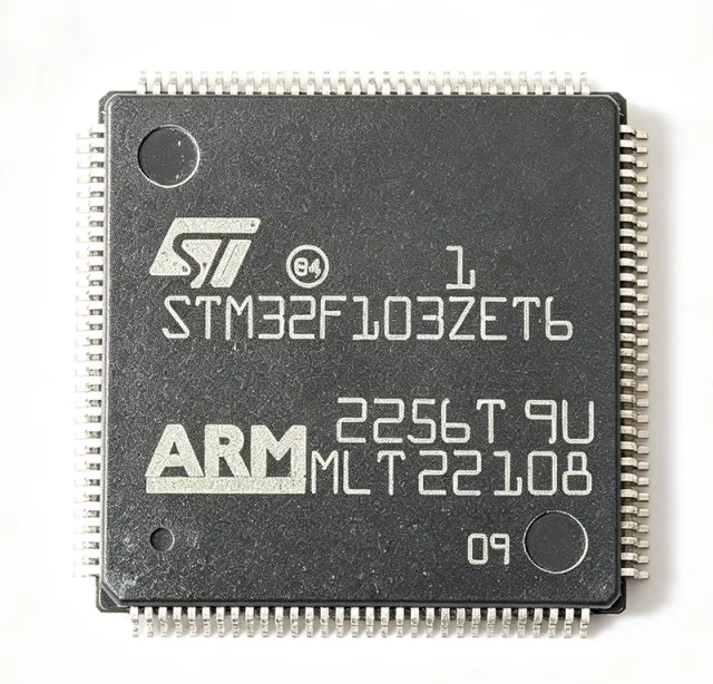
STM32F103ZET6 - 72MHz Cortex-M3 MCU 512KB Flash | STMicroelectronics
STM32F103ZET6

STM32F103ZET6 - 72MHz Cortex-M3 MCU 512KB Flash | STMicroelectronics

The STMicroelectronics STM32F103ZET6 is a high-density performance line 32-bit microcontroller built on the ARM Cortex-M3 core running at up to 72 MHz, with 512 KB of Flash memory, 64 KB of SRAM, and 112 GPIOs in a 144-pin LQFP (20 x 20 mm) package operating from a 2.0 V to 3.6 V supply. A microcontroller (MCU) is a compact integrated circuit that combines a processor core, memory, and programmable peripherals on a single chip to govern a specific operation in an embedded system. MCUs sit at the heart of the embedded electronics hierarchy - from the ARM Cortex-M processor core, through the STM32 family of 32-bit microcontrollers, up to complete embedded control systems used in industrial automation, consumer devices, and IoT products. Key features include three 12-bit ADCs with up to 21 channels, two 12-bit DACs, a 12-channel DMA controller, and an unusually rich communication set: up to 5 USARTs, 3 SPIs, 2 I2Cs, 1 CAN 2.0B, 1 USB 2.0 Full-Speed, and 1 SDIO interface. The Cortex-M3 core delivers 1.25 DMIPS/MHz (Dhrystone 2.1), giving roughly 90 DMIPS at 72 MHz, while the Nested Vectored Interrupt Controller (NVIC) provides low-latency deterministic interrupt handling. Architecturally, the device integrates advanced-control, general-purpose, and basic timers (including PWM timers for motor control), a real-time clock (RTC), and a CRC calculation unit. Both JTAG and Serial Wire Debug (SWD) interfaces are supported, and boot can be selected from Flash, system memory, or SRAM. The 512 KB Flash and 112 GPIOs of the LQFP144 make it the largest-pin, largest-memory STM32F103 variant, ideal for complex firmware with real-time control and multiple communication stacks. Typical applications include industrial control and PLC systems, motor drives, medical devices, communication boards, and IoT gateways. The wide 2.0 V to 3.6 V supply range and -40C to +85C operating temperature support both battery-powered and industrial designs. When designing with this device, decouple every VDD pin with 100 nF ceramic capacitors placed close to the pins plus one bulk capacitor, and filter VDDA with a ferrite bead to protect the 12-bit ADC noise floor. The BOOT0/BOOT1 pins must be strapped correctly at reset to select the desired boot source. This page adds value beyond the ST datasheet by synthesizing drop-in alternatives (GD32F103ZET6, APM32E103ZET6), pricing tiers, engineering design notes, and application guidance in one citable reference.

USD $5.39 संपर्क
STM32F103ZET6TR - 72MHz Cortex-M3 MCU 512KB Flash | STMicroelectronics (Tape & Reel)
STM32F103ZET6TR

STM32F103ZET6TR - 72MHz Cortex-M3 MCU 512KB Flash | STMicroelectronics (Tape & Reel)

The STMicroelectronics STM32F103ZET6TR is a high-density performance line 32-bit microcontroller built on the ARM Cortex-M3 core running at up to 72 MHz, with 512 KB of Flash memory, 64 KB of SRAM, and 112 GPIOs in a 144-pin LQFP (20 x 20 mm) package operating from a 2.0 V to 3.6 V supply. A microcontroller (MCU) is a compact integrated circuit that combines a processor core, memory, and programmable peripherals on a single chip to govern a specific operation in an embedded system. MCUs sit at the heart of the embedded electronics hierarchy - from the ARM Cortex-M processor core, through the STM32 family of 32-bit microcontrollers, up to complete embedded control systems used in industrial automation, consumer devices, and IoT products. Key features include three 12-bit ADCs with up to 21 channels, two 12-bit DACs, a 12-channel DMA controller, and an unusually rich communication set: up to 5 USARTs, 3 SPIs, 2 I2Cs, 1 CAN 2.0B, 1 USB 2.0 Full-Speed, and 1 SDIO interface. The Cortex-M3 core delivers 1.25 DMIPS/MHz (Dhrystone 2.1), giving roughly 90 DMIPS at 72 MHz, while the Nested Vectored Interrupt Controller (NVIC) provides low-latency deterministic interrupt handling. Architecturally, the device integrates advanced-control, general-purpose, and basic timers (including PWM timers for motor control), a real-time clock (RTC), and a CRC calculation unit. Both JTAG and Serial Wire Debug (SWD) interfaces are supported, and boot can be selected from Flash, system memory, or SRAM. The 512 KB Flash and 112 GPIOs of the LQFP144 make it the largest-pin, largest-memory STM32F103 variant, ideal for complex firmware with real-time control and multiple communication stacks. Typical applications include industrial control and PLC systems, motor drives, medical devices, communication boards, and IoT gateways. The wide 2.0 V to 3.6 V supply range and -40C to +85C operating temperature support both battery-powered and industrial designs. When designing with this device, decouple every VDD pin with 100 nF ceramic capacitors placed close to the pins plus one bulk capacitor, and filter VDDA with a ferrite bead to protect the 12-bit ADC noise floor. The BOOT0/BOOT1 pins must be strapped correctly at reset to select the desired boot source. This page adds value beyond the ST datasheet by synthesizing drop-in alternatives (GD32F103ZET6, APM32E103ZET6), pricing tiers, engineering design notes, and application guidance in one citable reference.

USD $5.39 संपर्क
STM32F103ZET7 - 72MHz Cortex-M3 512KB MCU | STMicroelectronics
STM32F103ZET7

STM32F103ZET7 - 72MHz Cortex-M3 512KB MCU | STMicroelectronics

The STMicroelectronics STM32F103ZET7 is a 32-bit ARM Cortex-M3 microcontroller operating at up to 72 MHz, with 512 KB of embedded Flash memory and USB, CAN, 11 timers, 3 ADCs, and 13 communication interfaces. It is packaged in a 144-LQFP 20 mm x 20 mm package. The STM32F103ZET7 belongs to STMicroelectronics’ high-density performance-line STM32F1 MCU family. A microcontroller is a programmable system-on-chip that integrates a processor core, memory, peripherals, and communication interfaces on one semiconductor device. The STM32F1 family combines an ARM Cortex-M3 RISC core with embedded control peripherals, making it suitable for industrial equipment, data acquisition, communications, motor control, and embedded automation. Its 32-bit architecture supports efficient control tasks and higher processing performance than many 8-bit or 16-bit alternatives. The STM32F103ZET7 provides 512 KB of Flash for firmware and 2.5 V/3.3 V operation as identified in the verified distributor and datasheet listings. Its feature set includes USB, CAN, 11 timers, 3 ADCs, and 13 communication interfaces. These resources allow one controller to coordinate analog measurement, timing, communication protocols, and control outputs while reducing the number of discrete components in a design. The device is identified as a 144-LQFP 20 mm x 20 mm surface-mount package. Its high pin count supports broad peripheral access and makes the STM32F103ZET7 useful for designs requiring numerous I/O functions, communications, and motor-control signals. The verified listing identifies the part as a 32-bit Cortex-M3 MCU with 72 MHz operation and 512 KB Flash memory. Typical applications include industrial control systems, IoT devices, embedded automation, motor control, metering equipment, USB-connected instrumentation, CAN-based nodes, and low-power embedded boards. Firmware selection should verify clock configuration, peripheral pin assignments, memory mapping, and the STM32F1 reference manual requirements before production release. This page combines verified manufacturer and distributor information with structured engineering guidance. Pricing, availability, lifecycle status, detailed electrical limits, and complete pin naming are not fully supplied in the retrieved data and must be confirmed against current manufacturer or distributor documentation before purchase or design approval.

RFQ संपर्क
STM32F103ZFH6 - 72MHz Cortex-M3 768KB MCU | STMicroelectronics
STM32F103ZFH6

STM32F103ZFH6 - 72MHz Cortex-M3 768KB MCU | STMicroelectronics

The STMicroelectronics STM32F103ZFH6 is a 32-bit ARM Cortex-M3 microcontroller with a maximum operating frequency of 72 MHz, 768 KB of Flash memory, and a 144-LFBGA 10 x 10 mm package. It also supports operation from a 2.5 V or 3.3 V supply, combining embedded Flash, SRAM, communication peripherals, timers, and analog conversion functions in one surface-mount device. A microcontroller is an integrated circuit that executes embedded software while coordinating digital inputs, outputs, communications, and analog measurements. Within the product hierarchy, the STM32F103ZFH6 is an ARM Cortex-M3 MCU, a 32-bit microcontroller, and a member of STMicroelectronics' STM32 embedded-processing family. It is intended for systems that require substantially more Flash memory and I/O than small 8-bit or 16-bit control devices. The verified product information identifies the STM32F103ZFH6 as a 72 MHz device with 768 KB of Flash organized as 768K x 8. Its 32-bit Cortex-M3 core provides the processing foundation for control loops, communications gateways, human-interface systems, and data acquisition. The 144-LFBGA package supplies 144 connection points in a compact 10 x 10 mm surface-mount footprint suitable for multilayer PCB designs. The STM32F103 family is associated with USB, CAN, six timers, two ADCs, and six communication interfaces. These functions support designs connecting external digital devices, transferring data over serial or network links, measuring analog signals, and controlling time-dependent peripherals. The available verified data does not specify individual GPIO counts, SRAM capacity, ADC resolution, or communication baud-rate limits, so those values must be confirmed in the manufacturer datasheet before final system design. Typical applications include industrial automation equipment, USB-connected embedded controllers, CAN network nodes, data-acquisition systems, motor and motion-control platforms, and communication equipment. The 72 MHz Cortex-M3 core can manage multiple interrupt-driven peripherals while the 768 KB Flash capacity accommodates larger embedded applications, protocol stacks, and application firmware. The principal design consideration is package and PCB complexity. A 144-LFBGA device requires a multilayer board, fine-pitch routing, controlled escape routing, and careful thermal management. Designers should also verify peripheral assignments, pin multiplexing, power sequencing, decoupling, and firmware support against the exact datasheet and reference manual before releasing hardware. This page consolidates verified distributor pricing, package details, technical attributes, sourcing links, and design guidance into one engineering-focused reference. It also distinguishes explicitly verified information from parameters that require confirmation from the manufacturer datasheet.

RFQ संपर्क
STM32F103ZFH6TR - 72MHz Cortex-M3 MCU | STMicroelectronics
STM32F103ZFH6TR

STM32F103ZFH6TR - 72MHz Cortex-M3 MCU | STMicroelectronics

The STMicroelectronics STM32F103ZFH6TR is a 32-bit ARM Cortex-M3 microcontroller operating at 72 MHz, with 768 KB of embedded Flash memory in a 144-LFBGA (10 x 10 mm) package. It combines a high-performance RISC core with integrated microcontroller peripherals in a compact surface-mount package suitable for space-constrained embedded products. A microcontroller is a programmable semiconductor device that executes firmware, reads sensors, controls actuators, and manages system communication. The STM32F103 product family belongs to the embedded-processing hierarchy: ARM Cortex-M3 core, 32-bit microcontroller, embedded controller, and semiconductor. The STM32F103ZFH6TR is intended for applications requiring more memory and package I/O than smaller STM32F103 variants while retaining the established Cortex-M3 architecture. The device features a 72 MHz maximum clock, 768 KB of Flash memory, and an operating supply range of 2.0 V to 3.6 V. The manufacturer listing identifies 37 I/O ports, an ARM 32-bit RISC architecture, and a 144-LFBGA package measuring 10 x 10 mm. Its performance-line positioning supports embedded control applications that require deterministic real-time execution, serial communication, mixed-signal measurement, and external peripheral control. Its 144-pin LFBGA construction provides a dense connection interface within a small footprint. The 0.5 mm ball pitch supports compact board layouts but requires careful PCB design, inspection, and assembly controls. The TR ordering suffix identifies a tape-and-reel shipping format, which supports automated manufacturing and volume production. Use the manufacturer pin-description table and land-pattern guidance when assigning every ball and defining the PCB footprint. Typical uses include industrial controllers, USB-connected data-acquisition equipment, CAN network nodes, motor-control systems, instrumentation, and communication gateways. The 768 KB Flash capacity is useful for firmware, configuration data, and application code, while the 72 MHz Cortex-M3 core provides the processing headroom required for concurrent peripheral control and protocol handling. The primary design consideration is package implementation. A 144-LFBGA assembly requires an HDI-capable board process, fine-pitch assembly capability, and careful power, ground, and signal-integrity layout. Confirm the exact ball assignments, exposed-pad requirements, and recommended PCB stackup in the manufacturer datasheet before releasing artwork. This product page consolidates the exact device identity, technical characteristics, compatible same-family options, practical application guidance, and PCB considerations into one engineering reference. It also supports structured sourcing through the Request a Quote form on this page for availability, lead-time, and order requirements.

RFQ संपर्क
STM32F103ZFT6 - 32-Bit 72MHz 768KB MCU | STMicroelectronics
STM32F103ZFT6

STM32F103ZFT6 - 32-Bit 72MHz 768KB MCU | STMicroelectronics

The STMicroelectronics STM32F103ZFT6 is a 32-bit ARM Cortex-M3 microcontroller with a 72 MHz maximum clock, 768 KB of Flash memory, and a 144-LQFP package measuring 20 mm by 20 mm. It belongs to the STM32F1 performance-line family and combines embedded control, communications, analog conversion, timer, and motor-control resources in one surface-mount device. An ARM Cortex-M3 microcontroller is a reduced-instruction-set embedded processor designed for real-time control systems. The Cortex-M3 core supplies deterministic instruction execution and interrupt handling, while the STM32F103 family integrates peripherals such as timers, communication interfaces, ADCs, USB, and CAN around that core. This hierarchy places the MCU above the processor core and into the broader embedded-control and semiconductor categories. The verified source data identifies the STM32F103ZFT6 as an XL-density member with 768 KB of Flash and a maximum frequency of 72 MHz. The same source states 1.25 DMIPS/MHz, supporting use in demanding embedded-control designs without requiring an external processor. Its large pin count also accommodates extensive I/O and peripheral connectivity compared with smaller STM32 packages. The manufacturer family description associates STM32F103 devices with USB, CAN, six timers, two ADCs, and six communication interfaces. These resources make the MCU suitable for gateways, motor controllers, industrial communication equipment, CAN or LIN-connected nodes, and embedded systems that require both control and communications. The verified data also lists vehicle gateway nodes and CAN/LIN networks as relevant use cases. A key engineering consideration is that the LQFP-144 footprint exposes substantially more interface pins than a compact MCU, enabling parallel I/O and multiple peripheral assignments while demanding careful PCB escape routing. Firmware and peripheral assignments should be validated against the manufacturer pinout and reference documentation before layout release. Alternate clock, memory, and analog behavior must also be checked when evaluating any substitute. This page combines verified distributor and manufacturer-linked source information, practical sourcing context, and structured MCU application guidance. It distinguishes the device’s confirmed 72 MHz and 768 KB attributes from parameters that remain unavailable, avoiding unsupported claims about electrical limits, temperature range, or compliance.

RFQ संपर्क