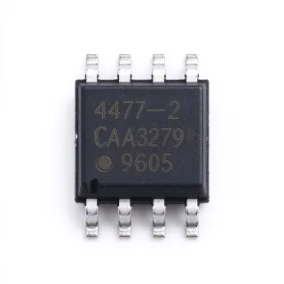
LT1007IS8 - Low-Noise Precision Op Amp | Analog Devices
MPN: LT1007IS8 ✓ सक्रियLT1007IS8 अवलोकन
A precision operational amplifier is a voltage-input analog integrated circuit that amplifies the difference between two input voltages. The LT1007 belongs to the operational-amplifier hierarchy, combining low-noise input stages, high open-loop gain, accurate offset behavior, and common-mode rejection. This makes it useful when a signal must be amplified without adding substantial noise or allowing supply variation and input offset to distort the result.
The principal performance feature is the LT1007 family's exceptionally low wideband noise density of 2.5 nV/√Hz. Its 1/f noise corner is 2 Hz, while the manufacturer describes 60 nV peak-to-peak noise from 0.1 Hz to 10 Hz. Precision is supported by 10 µV offset voltage, 0.2 µV/°C drift, and 130 dB common-mode and power-supply rejection. The LT1007 is optimized for low-noise signal conditioning rather than the very high gain-bandwidth operation of the decompensated LT1037.
The LT1007IS8's 8 MHz gain bandwidth provides useful bandwidth for audio, instrumentation, sensor, and control signals. Because the gain-bandwidth product limits closed-loop bandwidth, higher closed-loop gains reduce usable bandwidth. Input and output stability, source resistance, capacitive loading, and the power-supply bypass network must therefore be considered together when establishing signal-chain performance.
Typical uses include low-level sensor amplification, audio preamplification, strain-gauge and bridge-based measurements, precision current-to-voltage conversion, and analog instrumentation. The low-noise characteristic is especially valuable when the source impedance is similar to or below a few hundred ohms, although source resistance, resistor noise, and input-bias-current error must be evaluated together.
A practical design should keep feedback resistors and sensitive input nodes physically compact, use low-noise resistors where appropriate, and place bypass capacitors close to the supply pins. The 8-lead SOIC footprint permits conventional surface-mount assembly, but thermal performance and output drive remain important when driving heavy loads or operating across the extended temperature range.
This page combines the manufacturer's precision and noise characteristics, package information, drop-in alternatives, application guidance, and design considerations to provide a practical engineering reference for selecting and implementing the LT1007IS8.
के लिए ड्रॉप-इन विकल्प LT1007IS8 — समान पैकेज, पिन-टू-पिन संगत। PCB रीवर्क आवश्यक करने वाले भिन्न-पैकेज पार्ट्स शामिल नहीं हैं।
LT1007IS8#PBF
✅ ड्रॉप-इन📋 संदर्भ विकल्प (कैटलॉग में नहीं)
LT1007CS8#PBF
✅ ड्रॉप-इन ⚠️ विनिर्देश असत्यापित📋 संदर्भ विकल्प (कैटलॉग में नहीं)
LT1007IS8 Maximum Ratings और Electrical Characteristics
| Amplifier Type | General-purpose precision operational amplifier |
| Number of Circuits | 1 circuit |
| Gain Bandwidth Product | 8 MHz |
| Wideband Noise Density | 2.5 nV/√Hz |
| 1/f Noise Corner Frequency | 2 Hz |
| 0.1 Hz to 10 Hz Peak-to-Peak Noise | 60 nV |
| Input Offset Voltage | 10 µV |
| Input Offset Drift | 0.2 µV/°C |
| Common-Mode Rejection | 130 dB |
| Power-Supply Rejection | 130 dB |
| सप्लाई वोल्टेज | ±15 V |
| ऑपरेटिंग तापमान रेंज | -55°C to +125°C |
| पैकेज | 8-lead SOIC |
| माउंटिंग प्रकार | Surface mount |
| Lead-Free Ordering Suffix | #PBF |
LT1007IS8 पिन कॉन्फ़िगरेशन
| पिन 1 | OFFSET NULL — Offset-voltage null terminal |
| पिन 2 | INVERTING INPUT — Inverting input terminal |
| पिन 3 | NONINVERTING INPUT — Non-inverting input terminal |
| पिन 4 | V− — Negative supply-voltage terminal |
| पिन 5 | OFFSET NULL — Offset-voltage null terminal |
| पिन 6 | OUTPUT — Analog output terminal |
| पिन 7 | V+ — Positive supply-voltage terminal |
| पिन 8 | NC — Not connected |
सामान्य अनुप्रयोग
LT1007IS8 के लिए उपयुक्त है 6 अनुप्रयोगs: Precision Bridge Sensor Amplification, Low-Level Audio Preamplification, Precision Current-to-Voltage Conversion, Industrial Sensor Signal Conditioning, Test and Measurement Front Ends, Control and Monitoring Analog Channels.
Precision Bridge Sensor Amplification
The LT1007IS8 is appropriate for amplifying the small differential voltage produced by strain gauges, load cells, and resistive bridges. Its 2.5 nV/√Hz noise density avoids adding substantial noise to the sensed signal, while 130 dB common-mode rejection helps suppress the larger common-mode voltage present across many bridges. An instrumentation-style circuit should still use matched resistors with low absolute tolerance and suitable temperature coefficients. The practical benefit is improved resolution at low excitation voltages, where amplifier offset and drift can otherwise dominate the measurement.
अनुशंसित
Low-Level Audio Preamplification
The LT1007IS8 can form the input stage of a low-noise audio preamplifier when source impedance and gain are suitable for an 8 MHz operational amplifier. Its 2.5 nV/√Hz noise density and 60 nV peak-to-peak 0.1 Hz to 10 Hz noise support quiet signal-chain design, especially for microphone or magnetic-head sources. Feedback-resistor Johnson noise and the source impedance must be included in the total noise calculation. The result is a precision preamp that preserves small signals without relying on an unnecessarily high closed-loop gain.
अनुशंसित
Precision Current-to-Voltage Conversion
The LT1007IS8 suits current-to-voltage conversion in sensors where the target input current is small and measurement resolution matters. A transimpedance stage can use the amplifier's low voltage noise and 10 µV offset specification, but total error also depends on the feedback resistor and input-bias current. Keep the feedback resistor value compatible with the required transimpedance and bandwidth, because gain and speed trade against one another. This arrangement is useful for photodiode, electrochemical-cell, and current-output sensor interfaces.
अनुशंसित
Industrial Sensor Signal Conditioning
The LT1007IS8 is appropriate for conditioning low-level industrial sensor outputs where offset drift and noise constrain useful measurement range. Its 0.2 µV/°C drift and 130 dB power-supply rejection reduce errors in systems with multiple supply rails or varying ambient temperature. The amplifier should be paired with stable feedback components and protected against transient input voltages. Compared with a general-purpose op amp, its precision-focused characteristics provide a clearer margin when the sensor output is close to the measurement noise floor.
अनुशंसित
Test and Measurement Front Ends
The LT1007IS8 can serve as a low-noise input amplifier in precision test equipment, buffer stages, and programmable measurement interfaces. Its 8 MHz gain bandwidth supports moderate-bandwidth signals, while the low-noise and precision specifications help preserve small test signals. Designers should account for gain-bandwidth distribution when using high closed-loop gain and should verify output-swing limits against the intended signal range. This role is especially useful when the front end must reject supply noise and common-mode disturbances without adding substantial broadband noise.
अनुशंसित
Control and Monitoring Analog Channels
The LT1007IS8 is usable in analog control or monitoring channels that process low-level feedback signals and require stable offset behavior. The combination of 130 dB common-mode rejection, low drift, and low wideband noise helps preserve control-loop accuracy when the monitored signal is small. Stable feedback resistors and careful grounding remain essential because their tolerance and noise directly influence closed-loop performance. The part is best treated as a precision analog building block rather than a high-current driver, so downstream buffer stages may be needed for heavier loads.
अनुशंसित
अनुशंसित उत्पादों का सारांश
के लिए इंजीनियरिंग संदर्भ डेटा LT1007IS8 — तुलना, डिज़ाइन मार्गदर्शन और अनुपालन जानकारी।
चयन गाइड
विकल्पों के साथ तुलना
| पैरामीटर | यह उत्पाद | LT1007IS8#PBF | LT1007CS8#PBF |
|---|---|---|---|
| Brand | Analog Devices | Analog Devices | Analog Devices |
| Package | 8-lead SOIC | 8-lead SOIC | 8-lead SOIC |
| Amplifier Type | Low-noise precision operational amplifier | Low-noise precision operational amplifier | Low-noise precision operational amplifier |
| Number of Circuits | 1 circuit | 1 circuit | 1 circuit |
| Gain Bandwidth Product | 8 MHz | 8 MHz | 8 MHz |
| Wideband Noise Density | 2.5 nV/√Hz | 2.5 nV/√Hz | 2.5 nV/√Hz |
| Input Offset Voltage | 10 µV | 10 µV | 10 µV |
| Input Offset Drift | 0.2 µV/°C | 0.2 µV/°C | 0.2 µV/°C |
| Common-Mode Rejection | 130 dB | 130 dB | 130 dB |
मुख्य विशेषताएँ
- Very low wideband noise for a precision operational amplifier (बनामLT1007CS8#PBF)
- Low offset and drift for low-level analog measurement (बनामLT1007CS8#PBF)
- Exact lead-free ordering form is available for the target circuit (बनामLT1007CS8#PBF)
डिज़ाइन नोट्स
Keep the inverting input, feedback components, and non-inverting input traces compact and away from high-current switching nodes. Place bypass capacitors close to the V+ and V− pins and provide a low-impedance ground return. These layout practices matter because the LT1007IS8's 2.5 nV/√Hz noise performance cannot be realized if board leakage, ground potential differences, or switching-node pickup dominate the input.
Do not select the amplifier from noise density alone. Calculate the total input-referred noise from the source impedance, feedback resistors, amplifier noise, and 1/f contribution. In addition, check that the intended closed-loop gain fits within the 8 MHz gain-bandwidth product and confirm output swing and load-current limits at the selected supply voltage.
The manufacturer documentation identifies ±15 V conditions for the stated precision and noise specifications. Before using the part with single-supply or lower-voltage operation, verify the applicable electrical-characteristics curves and output-swing behavior. Avoid using the ±15 V test condition as an indication that every function or limit is identical at other supply voltages.
Although the SOIC-8 package supports compact surface-mount layouts, power dissipation and output drive depend on the selected feedback network, load, supply voltage, and ambient temperature. For continuous heavy-load operation, calculate dissipation from the actual output current and voltage drop, then verify the junction-temperature margin under the board's worst-case thermal conditions.
अनुपालन जानकारी
The #PBF ordering suffix identifies a lead-free form. Separate RoHS, REACH, halogen-free, conflict-minerals, and automotive qualification declarations were not stated in the supplied product information and therefore remain unknown. AEC-Q100 is not applicable to the standard industrial-temperature device.