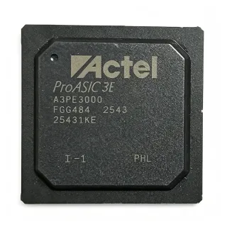
XC6SLX25T-4FGG484C - Spartan-6 LXT 24,051-Cell FPGA | Xilinx
MPN: XC6SLX25T-4FGG484C ✓ सक्रियXC6SLX25T-4FGG484C अवलोकन
An FPGA is a programmable digital logic device that replaces a combination of fixed-function gate arrays, interface controllers, and programmable glue logic. Within the semiconductor hierarchy, the XC6SLX25T-4FGG484C belongs to the Spartan-6 LXT FPGA family, a programmable-logic category combining configurable logic blocks, embedded block RAM, programmable I/O, and dedicated digital signal processing resources. Its large 484-ball package also exposes high-speed serial and parallel interfaces for communications and industrial-control equipment.
Key device attributes include 1,879 configurable logic blocks, 24,051 logic cells, 250 user I/O, and 958,464 total RAM bits. The 45 nm fabrication process supports a compact, high-performance implementation of parallel logic, memory, and dedicated serial transceivers. The LXT variant is intended for designs that need more connectivity than basic Spartan-6 LX devices while retaining the low-power programmable-logic architecture.
Typical uses include industrial Ethernet interfaces, data acquisition systems, video-processing pipelines, communications equipment, and embedded control platforms. The 250 I/O count supports external memory, parallel sensors, display controllers, and high-speed transceiver connections. Because the device uses a fine-pitch 484-ball BGA, its usefulness depends on multilayer PCB routing capability, controlled power delivery, and assembly processes capable of handling the package pitch.
A critical design consideration is that a faster or differently temperature-graded Spartan-6 LXT part must be checked against the original schematic, pinout, configuration design, and power-budget assumptions. The AMD Spartan-6 package pinout files remain the controlling reference for land patterns, ball assignments, and board-layout verification before a substitution is approved.
के लिए ड्रॉप-इन विकल्प XC6SLX25T-4FGG484C — समान पैकेज, पिन-टू-पिन संगत। PCB रीवर्क आवश्यक करने वाले भिन्न-पैकेज पार्ट्स शामिल नहीं हैं।
XC6SLX25T-2FGG484C
✅ ड्रॉप-इनकीमत के लिए संपर्क करें
डेटाशीट देखें →XC6SLX25T-3FGG484C
✅ ड्रॉप-इन📋 संदर्भ विकल्प (कैटलॉग में नहीं)
XC6SLX25T-N3FGG484C
✅ ड्रॉप-इन📋 संदर्भ विकल्प (कैटलॉग में नहीं)
XC6SLX25T-4FGG484I
✅ ड्रॉप-इन📋 संदर्भ विकल्प (कैटलॉग में नहीं)
XC6SLX25T-2FGG484I
✅ ड्रॉप-इन📋 संदर्भ विकल्प (कैटलॉग में नहीं)
XC6SLX25T-4FGG484C Maximum Ratings और Electrical Characteristics
| Device Type | Spartan-6 LXT Field Programmable Gate Array (FPGA) |
| Logic Cells | 24,051 cells |
| Configurable Logic Blocks | 1,879 CLBs |
| User I/O Count | 250 I/O |
| Total RAM | 958,464 bits |
| Process Technology | 45 nm |
| Core Supply Voltage | 1.2 V |
| Speed Grade | -4 |
| Package Type | 484-FBGA |
| Package Pin Count | 484 balls |
| Package Dimensions | 15 x 15 mm |
| Package Pitch | 0.80 mm |
| ऑपरेटिंग तापमान | 0°C to 85°C |
| माउंटिंग प्रकार | Surface Mount |
| Lead-Free Status | Lead-free package |
| Programmable Logic | Configurable logic blocks with embedded block RAM and DSP resources |
XC6SLX25T-4FGG484C 0.80 mm पिन कॉन्फ़िगरेशन गाइड
XC6SLX25T-4FGG484C (0.80 mm पैकेज) के लिए पिन कॉन्फ़िगरेशन। इस डिजिटल IC में GPIO, संचार इंटरफ़ेस (UART, SPI, I2C) और पावर पिन शामिल हैं। वैकल्पिक पिन फ़ंक्शन और कॉन्फ़िगरेशन विकल्पों के लिए निर्माता डेटाशीट देखें। एम्बेडेड सिस्टम डिज़ाइन और PCB लेआउट के लिए आवश्यक।

इसके लिए कोई विस्तृत pinout data उपलब्ध नहीं: XC6SLX25T-4FGG484C.
देखें डेटाशीट पूर्ण पिन कॉन्फ़िगरेशन के लिए।
सामान्य अनुप्रयोग
XC6SLX25T-4FGG484C के लिए उपयुक्त है 6 अनुप्रयोगs: Industrial Ethernet Control, Industrial Data Acquisition, Video and Image Processing, Communications Equipment, Embedded Control Platform, Programmable Logic Consolidation.
Industrial Ethernet Control
The XC6SLX25T-4FGG484C fits industrial Ethernet and networked-control designs that need programmable logic alongside high-speed serial connectivity. Its 24,051 logic cells can implement protocol state machines, packet buffers, filtering logic, and supervisory functions, while 958,464 RAM bits support queues and frame storage. The 250 I/O provide additional parallel control and status channels. Placing the device in the 484-ball package keeps high-speed serial and parallel interfaces on one component, but the board must satisfy fine-pitch escape-routing and multilayer return-path requirements. Timing closure for industrial link rates and margin analysis across temperature are essential before hardware release.
अनुशंसित
Industrial Data Acquisition
The XC6SLX25T-4FGG484C is suitable for multi-channel data-acquisition front ends where sensor outputs, counters, and digital interfaces must be coordinated in real time. The 24,051 logic cells provide enough parallel processing capacity for sampling control, trigger logic, and digital filtering, while the 958,464 RAM bits accommodate staged sample data and control structures. Its 250 I/O support parallel sensors, clocks, and external interfaces without requiring a separate large glue-logic device. Design the FPGA around deterministic clocking, register pipelining, and bounded acquisition latency, then verify power and timing against the -4 speed grade rather than assuming the behavior of a faster device.
अनुशंसित
Video and Image Processing
The XC6SLX25T-4FGG484C can support parallel video pipelines, pixel pre-processing, color conversion, and interface timing. Its programmable logic capacity allows fixed-function video functions to be combined with control logic, while block RAM provides line buffers, frame-staging memory, and lookup tables. The 250 I/O count is useful for parallel pixel and sync interfaces, and the LXT family includes dedicated high-speed resources for external data movement. Engineers should constrain output timing carefully because the -4 speed grade has less timing headroom than -2 or -3 alternatives. PCB signal-integrity work is equally important because high-volume pixel buses can couple into adjacent layers at 0.80 mm ball pitch.
अनुशंसित
Communications Equipment
The XC6SLX25T-4FGG484C fits communications equipment that combines packet handling, backplane interfaces, and dedicated serial connectivity. The 24,051 logic cells can support framing, filtering, rate conversion, and supervisory state machines, while 958,464 RAM bits provide packet buffering and deskew storage. Its 250 I/O leave room for parallel buses and legacy interfaces in addition to high-speed serial links. The design should use device-specific constraints for each serial transceiver and clock lane, preserve the recommended power and ground distribution, and confirm that the selected bitstream and speed grade satisfy line-rate timing before the layout is released for fabrication.
अनुशंसित
Embedded Control Platform
The XC6SLX25T-4FGG484C works well as the central programmable controller of an embedded platform containing parallel I/O, local memories, timers, and serial links. The 24,051 logic cells allow control firmware logic and hardware accelerators to coexist, while 958,464 RAM bits support local buffers, trace storage, or data queues. Its 250 I/O can connect external memories, sensors, actuators, and safety-monitoring signals. Firmware developers should define clock domains and reset behavior explicitly, isolate high-current switching loads from sensitive FPGA rails, and use the manufacturer's package files when planning the 484-ball footprint and power delivery network.
अनुशंसित
Programmable Logic Consolidation
The XC6SLX25T-4FGG484C can consolidate several fixed-function devices into one programmable platform, simplifying board partitioning and providing configurable interfaces. With 24,051 logic cells, 958,464 RAM bits, and 250 I/O, it can combine protocol conversion, glue logic, test control, and parallel data paths. Consolidation reduces the number of interconnects and creates a more flexible debugging environment through one programmable device. The engineering trade-off is a more demanding board layout: engineers must plan power delivery, decouple each supply properly, route high-speed signals with controlled return paths, and validate every mapped package ball against the AMD pinout files.
अनुशंसित
अनुशंसित उत्पादों का सारांश
के लिए इंजीनियरिंग संदर्भ डेटा XC6SLX25T-4FGG484C — तुलना, डिज़ाइन मार्गदर्शन और अनुपालन जानकारी।
चयन गाइड
विकल्पों के साथ तुलना
| पैरामीटर | यह उत्पाद | XC6SLX25T-2FGG484C | XC6SLX25T-3FGG484C | XC6SLX25T-N3FGG484C | XC6SLX25T-4FGG484I | XC6SLX25T-2FGG484I |
|---|---|---|---|---|---|---|
| Brand | Xilinx | Xilinx | Xilinx | Xilinx | Xilinx | Xilinx |
| Package | 484-FBGA | 484-FBGA - same | 484-FBGA - same | 484-FBGA - same | 484-FBGA - same | 484-FBGA - same |
| Device Family | Spartan-6 LXT | Spartan-6 LXT | Spartan-6 LXT | Spartan-6 LXT | Spartan-6 LXT | Spartan-6 LXT |
| Speed Grade | -4 | -2 | -3 | -3N | -4 | -2 |
| Logic Cells | 24,051 cells | 24,051 cells | 24,051 cells | 24,051 cells | 24,051 cells | 24,051 cells |
| User I/O Count | 250 I/O | 250 I/O | 250 I/O | 250 I/O | 250 I/O | 250 I/O |
| Total RAM | 958,464 bits | 958,464 bits | 958,464 bits | 958,464 bits | 958,464 bits | 958,464 bits |
| Process Technology | 45 nm | 45 nm | 45 nm | 45 nm | 45 nm | 45 nm |
| Core Supply Voltage | 1.2 V | 1.2 V | 1.2 V | 1.2 V | 1.2 V | 1.2 V |
मुख्य विशेषताएँ
- Retains the -4 speed grade while changing the temperature-grade suffix (बनामXC6SLX25T-4FGG484I)
- Provides additional timing margin in the same footprint (बनामXC6SLX25T-2FGG484C)
- Intermediate same-package performance option (बनामXC6SLX25T-3FGG484C)
- Supports a distinct same-package speed designation (बनामXC6SLX25T-N3FGG484C)
डिज़ाइन नोट्स
Use the AMD Spartan-6 package device pinout files as the controlling reference for the 484-ball FGG land pattern, ball assignments, and board dimensions. A 0.80 mm pitch package requires reliable fan-out from the inner balls, adequate via-in-pad or via-construction rules, and plane geometry that preserves escape routing. After component placement, compare the actual pad coordinates against the manufacturer package file rather than relying on a generic BGA footprint.
Separate the 1.2 V core rail from I/O and auxiliary supply requirements using the power architecture defined for the selected Spartan-6 device. Place local bypass capacitors close to their associated supply balls, preserve the recommended current-return paths, and avoid routing high-current or switching returns beneath the FPGA. Verify each rail's steady-state and transient requirement against the implemented design rather than deriving the complete power plan from the core voltage alone.
Apply device-specific timing constraints to clocks, high-speed serial lanes, and wide parallel buses. For each major interface, confirm that the selected -4 speed grade closes timing over the required voltage and temperature conditions. Use controlled-impedance routing, continuous reference planes, and appropriate via stitching, then run post-layout signal-integrity checks on the highest-failure-risk nets before releasing the board for fabrication.
Do not treat a same-package Spartan-6 ordering code as an automatic drop-in substitute. Speed suffixes change performance and power behavior, temperature suffixes change the intended operating range, and configuration support or ordering status may differ. Before substitution, verify the exact MPN in the FPGA design tool, rerun timing and bitstream generation, compare the AMD package files, and confirm procurement availability for the complete ordering code.
अनुपालन जानकारी
The FGG package is identified as lead-free in the device listing. RoHS, REACH, halogen-free, and conflict-minerals statements were not confirmed for the exact MPN, so those fields remain unknown. AEC-Q100 qualification is not applicable to this commercial Spartan-6 FPGA ordering code.