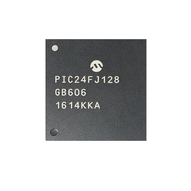
What is the PIC24FJ128GB606-E/MR, and is it currently available?
The PIC24FJ128GB606-E/MR is a Microchip Technology 16-bit PIC24F microcontroller with a maximum CPU frequency of 32 MHz, 128 KB of dual-partition Flash, 32 KB of RAM, and an integrated USB 2.0 full-speed OTG controller with an on-chip PHY. It operates from 2.0 V to 3.6 V and is packaged in a 64-pin VQFN measuring 9 x 9 mm with an exposed thermal pad. The device is AEC-Q100 qualified for automotive applications and rated for -40 C to +125 C operation. Current availability is 12,000 units with an MOQ of 1 as of 2026-11-01. Its lifecycle status is NRND, so buyers should use the available inventory for existing designs while obtaining sourcing confirmation for new production commitments. The database also lists a $3.78 base price and a separate quantity schedule beginning at $6.42 for one unit as of 2026-11-01; both values are reported here rather than silently treating them as the same price point.
View the PIC24FJ128GB606-E/MR product record for the complete database entry, or browse the XAIPART component catalog when reviewing the available inventory position.
How do you select and design in the PIC24FJ128GB606-E/MR?
Start with the requirements that distinguish this MCU: USB connectivity, updateable firmware, low-power operation, analog measurement, and an exposed-pad VQFN layout. The PIC24F core uses a modified-Harvard architecture with 16-bit data and a 24-bit instruction word. Peripheral Pin Select remapping allows functions to be assigned to remappable I/O pins, which helps designers route the PCB around fixed USB, oscillator, programming, and reference functions.
Which verified specifications drive component selection?
| Selection area | Verified specification | Engineering significance |
|---|---|---|
| Core and architecture | PIC24F, 16-bit RISC modified-Harvard; 16-bit data; 24-bit instruction word | Supports a 16-bit embedded control design with a 24-bit instruction word. |
| Maximum CPU frequency | 32 MHz | Sets the maximum processing clock for the selected operating conditions. |
| Program memory | 128 KB, organized as 43K x 24, with dual-partition Flash and Live Update | Supports field-firmware updates while the application continues running from the inactive partition. |
| RAM | 32 KB | Provides data memory for application and USB buffering requirements. |
| Supply voltage | 2.0 V to 3.6 V | Defines the operating range for Vcc/Vdd rail design. |
| USB | USB 2.0 full-speed OTG with on-chip PHY | Integrates the USB interface and removes the need for an external full-speed PHY. |
| ADC | 10/12-bit resolution, up to 16 channels | Supports analog sensor and front-end sampling. |
| Timers | Five 16-bit timers/counters | Provides timing resources for control, measurement, and peripheral functions. |
| Communications | UART, SPI, I2C, PMP, and RTCC | Covers serial buses, parallel expansion, and calendar timing functions. |
| I/O | Up to 53 pins | Provides dedicated remappable and fixed-function connectivity. |
| Package | 64-pin VQFN, MR package, 9 x 9 mm, exposed thermal pad | Requires an exposed-pad PCB footprint and an adequate copper pour. |
| Temperature | -40 C to +125 C, E grade | Supports extended-temperature equipment requirements. |
| Automotive qualification | AEC-Q100 qualified | Provides a documented qualification basis for automotive designs. |
| Environmental compliance | ROHS3 compliant | Records the device's stated RoHS compliance status. |
| Moisture sensitivity | MSL 3, 168-hour floor life | Sets the handling requirement for the packaged component. |
Takeaway: Select this MCU when the design specifically benefits from integrated USB OTG, 32 MHz performance, dual-partition Live Update, and extended-temperature operation; verify the complete electrical and qualification requirements before treating it as a new-design choice.
How should the 2.0 V to 3.6 V supply be implemented?
Design the power rail within the verified 2.0 V to 3.6 V Vcc/Vdd range. The verified product guidance calls for a 100 nF plus 10 uF decoupling network near each supply pin according to Microchip application note AN584. The exact placement and component selection should follow the current datasheet and application guidance for the assembled board rather than relying on a generic bulk-capacitor rule.
The USB section adds dedicated pins that the PCB layout must preserve: D+ on pin 30, D- on pin 31, VBUS on pin 32, and VUSB3V3 on pin 33. Do not treat VUSB3V3 as interchangeable with a general Vdd pin. Its database name identifies it as the internal USB 3.3 V regulator output, while the MCU's general Vdd pins are identified separately.
For an energy-limited design, evaluate the XLP sleep specification in the operating mode that matches the production firmware. The verified FAQ reports sleep currents typically below 20 nA in deep Sleep with the RTCC running and identifies a 32 kHz secondary oscillator for timing during sleep. It also states that Microchip associates this low-power capability with more than 10 years of coin-cell operation in applicable sensor and IoT designs. Treat the battery-life statement as a design target rather than a universal result because the final runtime depends on the application workload and duty cycle.
Takeaway: Build the supply and USB layout from the verified pin functions first: support a 2.0 V to 3.6 V rail, place the recommended 100 nF plus 10 uF network near each supply pin, and preserve the dedicated D+, D-, VBUS, and VUSB3V3 connections.
How does Live Update change the firmware architecture?
The 128 KB Flash is organized as two 64 KB partitions with Live Update support. The application can continue running from the active partition while a new image is programmed into the inactive partition. After verification, the device changes to the new image without an application reboot or the update-induced downtime that a conventional single-bank design can experience.
Use the dual-image partition arrangement required by Live Update in the linker configuration. Treat the inactive bank as reserved for update operations rather than ordinary application storage. The verified applications identify industrial sensor hubs, automotive body modules, portable medical and fitness equipment, and USB-provisioned IoT nodes as suitable use cases because these systems benefit from firmware maintenance without interrupting their primary function.
| Live Update design item | Verified basis | Action for the design team |
|---|---|---|
| Flash organization | 128 KB, 43K x 24, dual partition | Reserve the inactive partition for the update image. |
| Bank size | Two 64 KB banks | Configure the linker and update process for the dual-image layout. |
| Update behavior | Application continues from the inactive partition; swap follows verification | Define image verification and recovery steps before field deployment. |
| Primary use cases | Industrial, medical, automotive, and USB-connected applications | Prioritize the MCU where uninterrupted operation during maintenance is valuable. |
Takeaway: Configure two 64 KB image banks and a verified update workflow before enabling Live Update in production; partitioning alone does not establish the update, rollback, and validation process.
Which pins need special attention on the 64-VQFN footprint?
The exposed thermal pad is pin 64 and must be soldered to a sufficient copper pour. Pin 1 is the package dot marker. Fixed or high-priority functions include the oscillator pins, MCLR, programming lines, USB pins, and ADC reference pins. The following selection identifies the functionally critical pins without reproducing the complete product-page pin table.
| Pin | Exact pin name | Design consideration |
|---|---|---|
| 7 | VDD | Positive supply voltage; include in decoupling and rail planning. |
| 6 | VSS | Ground connection. |
| 13 | OSC1/RC12 | Crystal oscillator input / Port C bit 12. |
| 14 | OSC2/RC13 | Crystal oscillator output / Port C bit 13. |
| 15 | SOSCO/RC14 | Secondary oscillator output / RTCC. |
| 16 | SOSCI/RC15 | Secondary oscillator input / RTCC. |
| 19 | MCLR | Master clear reset input. |
| 22 | PGED1/RP22 | Programming data line 1 / remappable I/O. |
| 23 | PGEC1/RP23 | Programming clock line 1 / remappable I/O. |
| 30 | D+ | USB D+ data line. |
| 31 | D- | USB D- data line. |
| 32 | VBUS | USB VBUS detect. |
| 33 | VUSB3V3 | USB internal 3.3 V regulator output. |
| 45 | AN0/RA0 | Analog input 0 / Port A bit 0. |
| 51 | VREF-/RA6 | ADC negative reference / Port A bit 6. |
| 52 | VREF+/RA7 | ADC positive reference / Port A bit 7. |
| 64 | VSS | Ground connection for the exposed thermal pad. |
For broader design workflow coverage, compare MCU prototyping practices in the XAIPART article on AI-assisted microcontroller prototyping. The product-specific decisions remain governed by the PIC24FJ128GB606 datasheet and the verified pinout.
Takeaway: Freeze the PCB footprint around the exact VQFN pin functions and exposed-pad requirement, then validate the oscillator, programming, USB, analog-reference, supply, and ground assignments against the official datasheet before layout release.
How do the USB, ADC, and communications peripherals affect architecture choice?
Use the integrated USB controller for device, host, or OTG designs that otherwise require an external full-speed PHY. The verified application data identifies HID, mass storage, CDC bridges, composite USB devices, and USB-connected provisioning as target functions. Full-speed operation is listed as 12 Mbps, and 128 KB of Flash plus 32 KB of RAM provides the stated memory base for USB class drivers, descriptors, application logic, and buffering.
For sensor hubs, the 16-channel 10/12-bit ADC can digitize compatible analog inputs, while UART, SPI, and I2C support external sensors and serial peripherals. Peripheral Pin Select remapping can reduce routing constraints by assigning supported functions to remappable pins. The ADC reference pins require deliberate PCB treatment because they are dedicated RA6 and RA7 functions in the supplied pinout.
The five 16-bit timers/counters and hardware CRC support timing, integrity, and control tasks without replacing the core CPU. The PMP and RTCC expand the device beyond a basic USB bridge. For a graphical interface on a separate MCU platform, the XAIPART article on MCU graphics without an operating system provides a separate design reference.
Takeaway: Map USB class, analog channels, serial buses, timers, and fixed-function pins during architecture review so the software feature set matches the available package connectivity without forcing avoidable PCB rerouting.
Which drop-in alternatives can replace the PIC24FJ128GB606-E/MR?
The verified alternatives list identifies the PIC24FJ1024GB606-I/MR as the supported comparison part. It has the same 64-VQFN footprint, the same PIC24F core, USB OTG, and 1 MB of Flash rather than 128 KB. Those shared attributes support PCB reuse, but they do not make the higher-density part a like-for-like memory substitution. Its RAM, supply range, temperature grade, qualification, and exact pin-level differences are not included in the supplied product data.
| Parameter | PIC24FJ128GB606-E/MR | PIC24FJ1024GB606-I/MR |
|---|---|---|
| Core | PIC24F 16-bit RISC modified-Harvard core | Same PIC24F core |
| Program memory | 128 KB, 43K x 24, dual-partition Flash with Live Update | 1 MB Flash |
| Flash capacity relative to primary device | Baseline | 8x larger |
| USB | USB 2.0 full-speed OTG with on-chip PHY | USB OTG |
| Package | 64-pin VQFN, MR, 9 x 9 mm, with exposed pad | Same 64-VQFN footprint |
The table intentionally does not copy the -40 C to +125 C rating, AEC-Q100 qualification, 32 KB RAM, 2.0 V to 3.6 V operating range, or pricing from the primary device onto the alternative. Those values were not provided as specifications for PIC24FJ1024GB606-I/MR. The verified FAQ also discusses the USB-free PIC24FJ128GA606-I/MR and the higher-density PIC24FJ1024GB606-I/MR as reuse options, but only the 1024GB606 part has comparison data in the alternatives block.
Use the PIC24FJ1024GB606-I/MR when the existing board can accept its memory configuration and the product's additional Flash is needed. Do not approve it as a drop-in substitute based only on the shared footprint. Confirm the unavailable parameters, especially electrical limits, qualification, and device-specific functions, from the manufacturer's complete documentation before release.
Takeaway: Treat the PIC24FJ1024GB606-I/MR as a footprint- and core-compatible candidate for PCB reuse, not as a fully qualified replacement until the parameters absent from the verified comparison have been confirmed.
What does the PIC24FJ128GB606-E/MR lifecycle and supply position mean for buyers?
The product's lifecycle status is NRND, which the verified FAQ identifies as Microchip's “Not Recommended for new designs” status. This status does not mean that inventory is unavailable: the database reports 12,000 units and an MOQ of 1. It does mean that procurement and engineering teams should avoid treating this exact suffix as the default choice for a new production release without confirming Microchip's roadmap and availability.
The quantity schedule provides exact unit pricing as of 2026-11-01:
| Quantity threshold | Verified unit price as of 2026-11-01 |
|---|---|
| 1 or more | $6.42 |
| 10 or more | $5.85 |
| 100 or more | $5.12 |
| 500 or more | $4.43 |
| 1,000 or more | $3.78 |
The database separately labels $3.78 as the base price. That label differs from the quantity schedule, which starts at $6.42 for a quantity of one. The table preserves the published tier structure rather than assuming that the base-price label applies to every single-unit order.
For existing production, use the available stock to plan consumption and replenishment. For a new design, evaluate the NRND position alongside an alternative strategy rather than assuming that current stock guarantees long-term continuity. The supplied data does not provide a production-life schedule, forecast, or dated end-of-life commitment.
Takeaway: Use the 12,000-unit inventory for supported existing demand, quote against the dated tier schedule, and secure a lifecycle review before selecting the NRND suffix for a new product launch.
What should buyers watch in the PIC24FJ128GB606-E/MR roadmap?
The strongest design watchpoints are already visible in the verified specifications: USB OTG integration, dual-partition Live Update, XLP sleep behavior, analog conversion, and a large remappable I/O count. These features shape product differentiation more reliably than unsupported market forecasts.
USB consolidation remains a practical selection driver because the MCU includes an on-chip PHY. A product that moves from a discrete USB interface to this MCU can reduce PHY component count, but the redesign must still preserve D+, D-, VBUS, and VUSB3V3. Full-speed operation is appropriate for the listed HID, mass storage, CDC, and provisioning roles. Firmware growth also needs attention: the 128 KB Flash includes two 64 KB Live Update banks, so application size and update-image size must fit the selected partition strategy.
Low-power differentiation depends on firmware and system behavior. The verified below-20 nA deep-sleep specification with RTCC running, combined with the 32 kHz secondary oscillator, supports designs that spend substantial time asleep. Evaluate wake sources, analog-sampling schedules, USB attachment behavior, and update frequency rather than using the sleep-current figure as a standalone battery-life prediction.
Analog and communications integration determine how much of a sensor hub remains on-chip. The MCU provides up to 16 ADC channels, UART, SPI, I2C, PMP, RTCC, five 16-bit timers, and up to 53 I/O pins. The product's 10/12-bit ADC should be matched to the required signal resolution, while dedicated reference pins and remappable I/O require an early package-level review.
For new platforms, the most important procurement question is not whether the feature set is attractive; it is whether the NRND lifecycle position fits the product's commercialization plan. Because the source data provides an alternative with 1 MB Flash and the same 64-VQFN footprint, teams that need substantially more code space can evaluate that device against the primary MCU without starting from an entirely unrelated package family.
Takeaway: Monitor three design constraints together—USB PHY integration, the two-bank 128 KB Flash budget, and the NRND supply position—and validate the 1 MB Flash alternative when application growth or lifecycle continuity outweighs like-for-like feature retention.
Komentar
Jadi orang pertama yang menulis komentar
🔐 Silakan masuk untuk mengirim komentar.
Tidak punya akun? Daftar