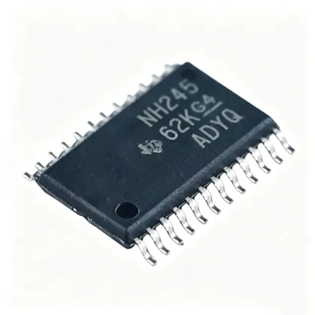
Produk (38.000+)

SN74LVC244APWR - Octal Buffer 3-State 24mA | TI | Bus Driver
SN74LVC244APWR

SN74LVC244APWR - Octal Buffer 3-State 24mA | TI | Bus Driver

The Texas Instruments SN74LVC244APWR is an octal buffer/line driver with 3-state outputs, designed for 1.65-V to 3.6-V VCC operation in a 20-pin TSSOP (PW) package rated from -40C to +125C. Organized as two 4-bit non-inverting buffers with separate active-low output-enable (OE) inputs, it provides asynchronous communication between data buses. A buffer/line driver is a digital logic IC that provides signal amplification, isolation, and fan-out between system blocks. Within the logic IC hierarchy, it belongs to the standard logic family alongside transceivers, latches, and flip-flops. The 3-state output feature lets the device disconnect from a shared bus, enabling multiple drivers to share a common data line without bus contention. Key features include a wide 1.65-V to 3.6-V supply range covering both 1.8-V and 3.3-V logic domains, inputs that tolerate voltages up to 5.5 V for mixed-voltage systems, and +/-24 mA output drive at 3.3 V. The Ioff partial-power-down circuitry prevents damaging backflow current when VCC is removed, and latch-up performance exceeds 100 mA per JESD 78 Class II. ESD protection exceeds 2000-V HBM (JESD 22 A114-A) and 1000-V CDM. Fabricated in advanced CMOS, the SN74LVC244A achieves a typical propagation delay of 4.3 ns at 3.3 V while maintaining low static power consumption, balancing speed and efficiency for bus-interface timing budgets. Typical applications include memory address buffering, clock distribution, and general-purpose I/O expansion for microcontrollers, FPGAs, and DSPs, plus level shifting between 1.8-V and 3.3-V domains in industrial control and telecommunications equipment. Design tip: decouple VCC with a 0.1-uF ceramic capacitor placed close to the pin, tie unused OE pins to a defined logic level, and keep traces short for high-speed signals.

Permintaan RFG Kontak
SN74LVC244QAPWRQ1 - Auto 8-Bit 3-State Buffer | TI
SN74LVC244QAPWRQ1

SN74LVC244QAPWRQ1 - Auto 8-Bit 3-State Buffer | TI

The Texas Instruments SN74LVC244QAPWRQ1 is an automotive-qualified (AEC-Q100) octal buffer/driver with 3-state outputs, organized as two independent 4-bit sections with separate output-enable (OE) inputs. It operates from a 1.65 V to 3.6 V supply in a 20-pin TSSOP (PW) surface-mount package with tape-and-reel packing. An octal buffer is a digital logic device that strengthens (buffers) eight signal lines at once, providing higher output drive and isolation between a controller and a load. Within the logic hierarchy, it belongs to the buffer/driver family of CMOS logic ICs, positioned above single-gate buffers and below bus transceivers, which add bidirectional capability. Key features include fully 3-state outputs for shared-bus connections, individual OE control for each 4-bit half, LVC-family CMOS technology supporting partial-power-down operation with Ioff protection, and an operating temperature range of -40C to +125C suitable for automotive and industrial environments. According to the TI SN74LVC244A-Q1 datasheet (Rev. D), the device performs the non-inverting buffer function Y = A for each channel. The LVC process provides low quiescent current, TTL-compatible input thresholds at 3.3 V operation, and balanced output drive for typical 24 mA-class loads at 3.3 V, making it suitable for address/data bus driving, clock distribution, and level-stable signal buffering between a microcontroller and peripherals. Typical applications include automotive body control modules, gateways and infotainment buses, industrial PLC I/O isolation, and memory or peripheral chip-select driving in embedded systems. Design tip: tie unused OE inputs to VCC through a pull-up resistor so outputs stay in the high-impedance state during power-up, and decouple the VCC pin with a 0.1 uF ceramic capacitor placed within 2 mm of the pin to suppress transient currents during simultaneous switching.

Permintaan RFG Kontak
SN74LVC2G125DCUR - Dual Bus Buffer 3-State Output | Texas Instruments
SN74LVC2G125DCUR

SN74LVC2G125DCUR - Dual Bus Buffer 3-State Output | Texas Instruments

The Texas Instruments SN74LVC2G125DCUR is a dual non-inverting bus buffer gate with 3-state outputs, integrating two independent 1-bit buffer/driver channels in an 8-pin VSSOP (DCU) package. Each channel operates across a wide 1.65 V to 5.5 V VCC supply range, supports ±24 mA output drive at 3.3 V, and features an active-low output-enable (OE) input that places the outputs in a high-impedance state when driven high. A bus buffer (also called a line driver or 3-state buffer) is a non-inverting signal-routing building block used to isolate a source from a shared bus, increase fan-out, or provide bidirectional control over which device drives a line. Buffers belong to the broader logic IC family (combinational logic), which sits under the digital semiconductor hierarchy. The SN74LVC2G125 implements LVC (Low-Voltage CMOS) technology, which is a sub-family of CMOS logic optimized for low static power and 5 V-tolerant I/O on mixed-voltage rails. Key features include a typical propagation delay (tpd) of 3.7 ns at 3.3 V, ±24 mA output drive capability (IoL/IoH) at 3.3 V, support of partial-power-down applications through Ioff circuitry that disables outputs to prevent backflow current, and an operating temperature range of -40 °C to +125 °C. The LVC2G family provides 5.5 V tolerance on the input pins even when VCC is lower, enabling level translation between 1.8 V, 3.3 V, and 5 V domains. From an architectural perspective, the device uses TI's EPIC (Enhanced-Performance Implanted CMOS) submicron process, giving it ESD protection exceeding 2000 V per MIL-STD-883 Method 3015 and 200 V using the machine model (C = 200 pF, R = 0 Ω). Each buffer consists of an input stage, an output-enable gate, and a 3-state CMOS output stage with controlled rise/fall symmetry. Typical applications include I2C/SPI bus isolation, point-to-point signal buffering on memory and module interfaces, GPIO expansion in microcontroller boards, level shifting between 1.8 V / 3.3 V / 5 V logic domains, and fan-out extension for low-drive clock or reset lines. The compact VSSOP-8 footprint makes it suitable for handheld and space-constrained designs. When designing with this device, ensure the OE pin is driven to a defined logic level (tie to GND through a pull-down if unused) to prevent the output from floating into a high-impedance state unintentionally. Decoupling VCC with a 0.1 µF ceramic capacitor placed within 5 mm of the supply pin is recommended for clean switching at high frequencies. This page synthesizes real-time distributor pricing, validated drop-in alternatives, and practical PCB design guidance for the SN74LVC2G125DCUR that goes beyond the manufacturer datasheet alone, helping engineers evaluate sourcing and design trade-offs at a glance.

Permintaan RFG Kontak
SN74LVC2G132YZPR - Dual 2-Input NAND Gate, Schmitt-Trigger, 8-DSBGA | Texas Instruments
SN74LVC2G132YZPR

SN74LVC2G132YZPR - Dual 2-Input NAND Gate, Schmitt-Trigger, 8-DSBGA | Texas Instruments

The Texas Instruments SN74LVC2G132YZPR is a dual 2-input NAND gate IC with Schmitt-trigger inputs, housed in an 8-pin DSBGA (NanoFree) wafer-level chip-scale package. The device operates from a 1.65 V to 5.5 V VCC supply, supports 5 V tolerant inputs up to 5.5 V, and provides two independent Schmitt-trigger NAND gates with ±24 mA output drive at 3.3 V. The Schmitt-trigger architecture gives different positive-going (VT+) and negative-going (VT-) input thresholds, providing superior noise immunity in harsh or slowly-changing input environments. A Schmitt-trigger NAND gate is a digital logic device that combines a NAND Boolean function with hysteresis at its input stage. NAND gates are universal logic primitives used to construct AND, OR, NOT, and any other Boolean function. Adding Schmitt-trigger hysteresis prevents oscillation when the input signal has slow edges or noise, which is critical in industrial, automotive, and battery-powered applications where supply rails can be noisy and rise/fall times are uncontrolled. Key features include 3.3 V typical low-power consumption of 10 µA ICC max, ±24 mA output drive at 3.3 V for driving heavily loaded buses, support for 5 V VCC operation, and an output ground bounce (VOLP) that meets LVC-family switching specifications. The DSBGA package is part of TI's NanoFree family, which eliminates lead-frame mass and provides a footprint as small as the silicon die itself, ideal for space-constrained handheld and wearable designs. The SN74LVC2G132 uses a standard CMOS implementation with CMOS-compatible inputs. The LVC logic family is designed for low-voltage, low-power operation while still delivering high drive strength. The device performs the Boolean function Y = A · B (active-low) in positive logic and is fully specified for partial-power-down applications with Ioff circuitry that prevents backflow current when the device is powered down but I/O lines remain active. Typical applications include portable consumer electronics, mobile handsets, tablet computing, industrial control logic, automotive body and infotainment modules, signal conditioning for noisy sensor lines, level shifting between low-voltage microcontrollers and 5 V peripherals, and wearable health monitors where board space is at a premium. The wide operating voltage range makes it compatible with 1.8 V, 2.5 V, 3.3 V, and 5 V system rails. When designing with this device, route input traces away from noisy power or switching nodes to take full advantage of Schmitt hysteresis. Bypass VCC with a 0.1 µF ceramic capacitor placed within 5 mm of the supply pin. Note that the DSBGA package requires precise PCB land pattern and reflow profile control; refer to TI application note SCBA017 for DSBGA handling guidelines. This page synthesizes distributor pricing, drop-in alternatives, and practical design notes not found in the manufacturer datasheet alone, including cross-reference information verified against TI product family listings and the Site MPN cross-reference database.

Permintaan RFG Kontak
SN74LVC2G17 - Dual Schmitt-Trigger Buffer 5.5V | Texas Instruments
SN74LVC2G17

SN74LVC2G17 - Dual Schmitt-Trigger Buffer 5.5V | Texas Instruments

The Texas Instruments SN74LVC2G17 is a dual Schmitt-trigger buffer designed for 1.65-V to 5.5-V VCC operation, performing the Boolean function Y = A on two independent channels. Packaged in the popular SOT-23-6 (DBV), SON-6 (DRY), and NanoStar (YEP) options, it suits space-constrained designs requiring noise-tolerant signal buffering. A Schmitt-trigger buffer is a digital logic gate that uses positive feedback to create different input thresholds for rising (VT+) and falling (VT-) signals. This hysteresis eliminates false triggering from noise or slow input edges, making Schmitt buffers essential for conditioning noisy signals, debouncing mechanical switches, and squaring up slow-rise-time waveforms. The SN74LVC2G17 belongs to the LVC logic family, part of the broader low-voltage CMOS buffer and line-driver category in the logic IC hierarchy. Key features include a wide supply range of 1.65 V to 5.5 V, 5.5-V input tolerance for mixed-voltage interfacing, and a maximum propagation delay (tpd) of 3.3 ns at 3.3 V. Output drive is ±24 mA at 3.3 V with a push-pull stage providing rail-to-rail output swing. Maximum ICC is 10 uA, enabling low-power designs, and the Ioff feature fully supports partial-power-down operation by preventing damaging backflow current when VCC is removed. Architecturally, the device uses a CMOS process with comparator-based Schmitt input circuits that guarantee stable switching even with very slow input transitions. Typical VOLP (output ground bounce) and VOHV (output VOH undershoot) are specified at 25C to characterize system-level signal integrity. Both an automotive SN74LVC2G17-Q1 (AEC-Q100 qualified) variant and the enhanced SN74LVC2G17-EP for demanding applications are available. Typical applications include switch debouncing, sensor signal conditioning, level shifting between 3.3-V and 5-V logic domains, and buffering of slow or noisy signals in industrial, consumer, and automotive electronics. Design tip: leverage the hysteresis characteristics for your noise environment and observe proper power sequencing - Ioff supports partial power-down, but unintended current paths should still be avoided.

Permintaan RFG Kontak
SN74LVC2G17DBVR - Dual Schmitt-Trigger Buffer 1.65V-5.5V | TI
SN74LVC2G17DBVR

SN74LVC2G17DBVR - Dual Schmitt-Trigger Buffer 1.65V-5.5V | TI

The Texas Instruments SN74LVC2G17DBVR is a dual-channel non-inverting Schmitt-trigger buffer housed in a 6-pin SOT-23 (DBV) package, designed for 1.65 V to 5.5 V VCC operation. Each channel performs the Boolean function Y = A and supports push-pull output drive with 32 mA of sink/source current, while the Schmitt-trigger inputs deliver separate positive-going (VT+) and negative-going (VT-) thresholds for high-noise-immunity signal conditioning. A Schmitt-trigger buffer is a type of logic buffer whose input stage uses positive feedback to create two distinct switching thresholds: VT+ for the rising edge and VT- for the falling edge. The hysteresis between these thresholds (typically around 0.5 V at 3 V VCC) rejects input noise and slow edges, making the device well suited for interfacing with mechanical switches, long PCB traces, or any signal that may be distorted by reflections and crosstalk. The SN74LVC2G17 sits in the LVC (Low-Voltage CMOS) logic family - a subcategory of standard logic ICs within the broader semiconductor hierarchy: logic gate -> buffer/driver -> 74-series logic -> integrated circuit. Key features include 5.5 V tolerant inputs that accept rails higher than VCC, an Ioff partial-power-down mode that disables outputs to prevent back-drive current when the device is unpowered, ±24 mA output drive at 3 V, and 4.4 ns typical propagation delay at 3.3 V. The NanoFree package technology eliminates traditional lead frames, and the SOT-23-6 footprint occupies just 2.9 mm x 1.6 mm of PCB area, enabling high-density designs in portable equipment. Typical applications include debouncing mechanical switches in consumer and industrial controls, buffering slow or noisy edges in sensor signal chains, single-direction level shifting between 1.8 V, 3.3 V and 5 V domains, fan-out for clock or reset lines, and LED or relay driver interfaces. The wide supply range also allows the part to operate across multiple rails in mixed-voltage systems. When designing with this device, place decoupling capacitors (0.1 uF ceramic typical) as close to VCC and GND as possible and keep input traces short to preserve noise margin. Because the outputs are push-pull CMOS, no external pull-up resistors are required and the device produces symmetrical rise and fall times into capacitive loads. This page synthesizes distributor stock and pricing, drop-in alternatives in the same SOT-23-6 footprint, and practical design notes that complement the TI datasheet's typical-application circuits.

Permintaan RFG Kontak
SN74LVC2G34DCKR - Dual Buffer 1.65-5.5V SC-70-6 | Texas Instruments
SN74LVC2G34DCKR

SN74LVC2G34DCKR - Dual Buffer 1.65-5.5V SC-70-6 | Texas Instruments

The Texas Instruments SN74LVC2G34DCKR is a dual non-inverting buffer gate designed for 1.65-V to 5.5-V VCC operation, performing the Boolean function Y = A in positive logic. It comes in a compact 6-pin SC-70 (DCK) surface-mount package measuring 2.0 mm x 1.25 mm with a 0.65-mm pin pitch. A buffer gate is a digital logic circuit that amplifies or isolates a signal without changing its logic level. In the logic IC hierarchy, it falls under gates within the 74LVC CMOS logic family, ultimately classified as a standard logic integrated circuit. Buffers increase fan-out, drive longer PCB traces, and provide impedance isolation between a signal source and its load. Key features include support for 5-V VCC operation, inputs tolerant up to 5.5 V regardless of supply, and a typical propagation delay (tpd) of 3.3 ns at VCC = 3.3 V. Output drive is +/-24 mA at 3.3 V, ensuring solid signal integrity. Maximum ICC is only 10 uA, making the part ideal for battery-powered designs. The device is fully specified for partial-power-down applications using Ioff circuitry, which disables outputs to prevent damaging backflow current when VCC is removed. The SN74LVC2G34 uses a CMOS process delivering high noise immunity and low static power dissipation. Typical VOLP (output ground bounce) and VOHV (undershoot) performance keeps switching noise minimal in mixed-signal boards. NanoStar and NanoFree package technologies are available in the family for ultra-miniature footprints. Typical applications include MCU GPIO buffering, clock distribution, level-compatible interfacing between 3.3-V and 5-V domains, and general logic isolation in consumer, industrial, and communication equipment. Pair it with TI translation parts such as TXS0102-Q1 or SN74LVC1T45 for full level shifting. Design tip: decouple VCC with a 0.1-uF ceramic capacitor close to the pin, and keep buffered traces short and impedance-controlled to preserve the 3.3-ns speed advantage.

Permintaan RFG Kontak
SN74LVC374A-Q1 - Octal D Flip-Flop, 3-State | Texas Instruments
SN74LVC374A-Q1

SN74LVC374A-Q1 - Octal D Flip-Flop, 3-State | Texas Instruments

The Texas Instruments SN74LVC374A-Q1 is an automotive-catalog octal edge-triggered D-type flip-flop with 3-state outputs, operating from a 1.65V to 3.6V supply (designed for 2.7V to 3.6V VCC operation) and available in 20-pin surface-mount packages including SOIC-20 (DW) and TSSOP-20 (PW). An octal D-type flip-flop is a sequential logic IC in the 74-series logic family that captures eight data bits simultaneously on the rising edge of a clock signal and holds them until the next clock edge. Within the logic hierarchy, it belongs to the flip-flop/latch category of CMOS integrated circuits, which sit inside the broader domain of digital logic ICs and semiconductor components. The 3-state outputs allow the device to be electrically disconnected from a shared bus, enabling multi-drop bus architectures. Key features include 3-state outputs designed specifically for driving highly capacitive or relatively low-impedance loads, 5.5V-tolerant input pins allowing safe interfacing with 5V logic systems, and typical output ground bounce (VOLP) and VOH undershoot (VOHV) specifications provided at VCC = 3.3V, 25C. As a high-drive CMOS device, it delivers 32 mA of drive current at 3.3V, making it ideal for driving multiple outputs and for high-speed applications up to 100 MHz, according to TI's SNx4LVC374A literature. The Q1 automotive-catalog variant is qualified for automotive environments and suits AEC-relevant designs. The architecture uses edge-triggered master-slave storage with a common clock (CP) pin and an active-low output-enable (OE) pin that controls all eight 3-state outputs independently of the clock. Typical applications include automotive body electronics, bus-interface buffering and data retention, register banks in instrumentation, and memory address/data latching where a shared 3-state bus is required. Design tip: tie the OE pin high through a pull-up resistor at power-up to keep the bus disconnected until the clock and data lines are stable, avoiding bus contention during system initialization.

Permintaan RFG Kontak
SN74LVC8T245PW - 8-Bit Dual-Supply Level Translator | TI (Tape & Reel)
SN74LVC8T245PW

SN74LVC8T245PW - 8-Bit Dual-Supply Level Translator | TI (Tape & Reel)

The Texas Instruments SN74LVC8T245PW is an 8-bit dual-supply bus transceiver with configurable voltage translation and 3-state outputs, packaged in a 24-pin TSSOP (PW) with Tape and Reel delivery. Both the VCCA and VCCB ports operate over the full 1.65V to 5.5V supply range, enabling bidirectional level translation between any combination of 1.8V, 2.5V, 3.3V, and 5V logic domains. A bus transceiver is a digital logic IC that moves data bidirectionally between two buses, with direction (DIR) and output-enable (OE) controls providing the handshake. The SN74LVC8T245 belongs to the voltage-level translator / logic IC hierarchy and is a member of the TI Widebus+ family, solving the classic mixed-voltage problem in systems where MCUs, FPGAs, and peripherals run on different rails. Key features include the fully configurable dual-rail architecture, 3-state outputs for bus sharing, mixed-mode signal operation (5V-tolerant I/O with reduced supply), and Ioff plus power-up 3-state support that blocks damaging backflow current during partial power-down and hot-insertion events. DIR and OE are referenced to VCCA, simplifying control-logic design. Technically, the device uses two independent supply-referenced port circuits with low-impedance LVC output drivers. The typical data rate of 100 Mbps supports SPI, I2C, UART, and parallel bus translation while preserving signal integrity with up to 15 pF load capacitance. Inputs accept voltages up to 5.5V regardless of supply level. Typical applications include level shifting for SD and SIM card interfaces, sensor and memory modules, 3.3V-to-5V industrial control I/O, and FPGA/CPLD I/O-bank adaptation to external peripherals. Design tip: decouple both VCCA and VCCB with 0.1uF ceramic capacitors placed close to the pins, tie OE to its proper logic level to avoid a 3-state bus at power-up, and set DIR according to data flow direction. Prices as of 2026-08-30.

USD $0,18 Kontak
SN74LVC8T245PWR - 8-Bit Dual-Supply Level Translator | TI
SN74LVC8T245PWR

SN74LVC8T245PWR - 8-Bit Dual-Supply Level Translator | TI

The Texas Instruments SN74LVC8T245PWR is an 8-bit dual-supply bus transceiver with configurable voltage translation and 3-state outputs, packaged in a 24-pin TSSOP (PW) with Tape and Reel delivery. Both the VCCA and VCCB ports operate over the full 1.65V to 5.5V supply range, enabling bidirectional level translation between any combination of 1.8V, 2.5V, 3.3V, and 5V logic domains. A bus transceiver is a digital logic IC that moves data bidirectionally between two buses, with direction (DIR) and output-enable (OE) controls providing the handshake. The SN74LVC8T245 belongs to the voltage-level translator / logic IC hierarchy and is a member of the TI Widebus+ family, solving the classic mixed-voltage problem in systems where MCUs, FPGAs, and peripherals run on different rails. Key features include the fully configurable dual-rail architecture, 3-state outputs for bus sharing, mixed-mode signal operation (5V-tolerant I/O with reduced supply), and Ioff plus power-up 3-state support that blocks damaging backflow current during partial power-down and hot-insertion events. DIR and OE are referenced to VCCA, simplifying control-logic design. Technically, the device uses two independent supply-referenced port circuits with low-impedance LVC output drivers. The typical data rate of 100 Mbps supports SPI, I2C, UART, and parallel bus translation while preserving signal integrity with up to 15 pF load capacitance. Inputs accept voltages up to 5.5V regardless of supply level. Typical applications include level shifting for SD and SIM card interfaces, sensor and memory modules, 3.3V-to-5V industrial control I/O, and FPGA/CPLD I/O-bank adaptation to external peripherals. Design tip: decouple both VCCA and VCCB with 0.1uF ceramic capacitors placed close to the pins, tie OE to its proper logic level to avoid a 3-state bus at power-up, and set DIR according to data flow direction. Prices as of 2026-08-30.

USD $0,18 Kontak
SN74LVC8T245QPWRQ1 - 8-Bit Auto Level Shifter | Texas Instruments
SN74LVC8T245QPWRQ1

SN74LVC8T245QPWRQ1 - 8-Bit Auto Level Shifter | Texas Instruments

The Texas Instruments SN74LVC8T245QPWRQ1 is an automotive-grade, 8-bit dual-supply bus transceiver with configurable voltage translation and 3-state outputs, supplied in a 24-pin TSSOP (PW) package. It is AEC-Q100 qualified for operation from -40C to +125C, making it suited for harsh automotive and industrial environments. A dual-supply bus transceiver is a logic component that moves data between two digital buses operating at different voltage levels. In the power-management and signal-chain hierarchy, it belongs to the level-translator family within the broader logic IC category. The SN74LVC8T245-Q1 uses two independent supply rails, VCCA and VCCB, each operable from 1.65V to 5.5V, enabling bidirectional translation between any two voltage domains, such as 1.8V MCUs communicating with 3.3V or 5V peripherals. Key features include direction-controlled (DIR) and output-enable (OE) pins supplied by VCCA, 3-state outputs for bus sharing, Ioff and power-up 3-state support for hot-insertion safety, and 5.5V-tolerant inputs. The device transmits data from A to B when B-port outputs are active, and from B to A otherwise, supporting asynchronous two-way bus communication with configurable translation on every bit. Architecturally, the device belongs to the TI LVC (Low-Voltage CMOS) family and the Widebus+ 8-bit format, combining fast propagation times at 3.3V with robust mixed-mode signal operation on all ports. Data-sheet-level design freedom comes from independent VCCA/VCCB pinout ordering, which simplifies PCB routing between voltage domains. Typical applications include automotive body and gateway ECUs translating MCU GPIO to CAN/LIN transceiver logic levels, infotainment and display module bus isolation, and industrial PLC I/O modules interfacing 3.3V controllers with 5V sensors. The 3-state outputs let multiple transceivers share one bus without contention. Design tip: tie OE high or low through a pull resistor at power-up to prevent bus contention, since the control pins are referenced to VCCA; ensure VCCA ramps before the uncontrolled bus is driven. This page synthesizes distributor pricing, drop-in alternatives, and practical design notes not found in the manufacturer datasheet. Pricing shown as of 2026-09-01.

USD $0,72 Kontak
SN74LVT244APWR - 3.3V ABT Octal Buffer/Line Driver | TI
SN74LVT244APWR

SN74LVT244APWR - 3.3V ABT Octal Buffer/Line Driver | TI

The Texas Instruments SN74LVT244APWR is a 3.3V ABT (Advanced BiCMOS Technology) octal buffer and line driver with 3-state outputs, housed in a 20-pin TSSOP (PW) package. It operates from a 2.7V to 3.6V supply, provides TTL-compatible input thresholds for 5V system interfacing, and is organized as two independent 4-bit buffers with separate output-enable (OE) inputs. A buffer and line driver is a digital logic IC that increases the drive current of a weak signal source so it can fan out to multiple loads or drive long bus lines. Within the semiconductor hierarchy, the SN74LVT244APWR belongs to the logic IC family, specifically buffers, drivers and receivers, under the broad category of integrated circuits. Line drivers sit between a microcontroller or FPGA bus and memory, peripherals, or backplanes, restoring signal integrity and isolating capacitive loading. Key features include non-inverting 3-state outputs that enter high impedance when disabled, allowing multiple devices to share a common bus; separate OE control for each 4-bit element, enabling half-width bus operation; LVT-speed propagation delays suited for address/data buffering; and 5V-tolerant TTL-level input logic so a 3.3V device can interface with legacy 5V systems. Technically, the ABT/LVT BiCMOS process combines the low static power of CMOS inputs with the high output drive of bipolar transistors, delivering strong sink and source current with fast edge rates while keeping supply current low in the static state. Typical applications include 8-bit address/data bus buffering in embedded systems, memory interface isolation, backplane line driving in industrial control, and 3.3V-to-5V TTL signal translation in mixed-voltage designs. Design consideration: tie unused OE inputs to VCC to guarantee outputs are enabled, and use short ground returns to limit ground bounce from fast bipolar output edges. This page synthesizes distributor availability, drop-in alternatives, pinout, and practical design notes not consolidated in the manufacturer datasheet.

Permintaan RFG Kontak
SN74LVTH16374-EP - 3.3V 16-Bit D Flip-Flop EP | Texas Instruments
SN74LVTH16374-EP

SN74LVTH16374-EP - 3.3V 16-Bit D Flip-Flop EP | Texas Instruments

The Texas Instruments SN74LVTH16374-EP is an Enhanced Product (EP) version of the 3.3-V ABT 16-bit edge-triggered D-type flip-flop with 3-state outputs. Designed for low-voltage 3.3-V VCC operation, the device provides TTL-level interface capability to 5-V system environments, making it well suited for defense, aerospace, and medical applications. It integrates sixteen positive-edge-triggered D-type flip-flops with common clock (CP) and output-enable (OE) controls in a space-saving 48-pin SSOP/TSSOP-style surface-mount package. A D-type flip-flop is a fundamental sequential logic element in the CMOS/TTL logic IC family hierarchy: it is a bistable storage circuit that captures the value at its D input on the rising edge of a clock signal and holds it at the Q output until the next clock edge. Sixteen-bit registered buffers like the SN74LVTH16374-EP belong to the broader categories of bus interface flip-flops, logic ICs, and digital semiconductors, providing pipeline registers, data latching, and bus isolation functions in digital systems. Key features include EP (Enhanced Product) qualification supporting defense, aerospace, and medical applications, 3.3-V operation with 5-V TTL-compatible inputs, 3-state outputs for bus-oriented applications, and ABT (Advanced BiCMOS Technology) combining CMOS low power with TTL drive capability and speed. The device is qualified against the standard SN74LVTH16374, with identical electrical behavior and pinout. Technically, the LVTH family uses BiCMOS process technology to achieve fast edge rates, balanced drive, and low dynamic power. The 3-state outputs place all sixteen Q outputs into a high-impedance state when OE is high, allowing multiple devices to share a common data bus. Edge-triggered clocking on the positive clock edge simplifies synchronous pipeline design versus level-sensitive latches. Typical applications include pipeline data registers in space-constrained avionics and defense electronics, bus isolation and buffering in medical imaging equipment, address/data latching in industrial control, and general-purpose 16-bit synchronous storage where EP-level reliability documentation is required. Design consideration: tie unused inputs to VCC or GND to prevent floating-node oscillation, and always bypass VCC with a 0.1-uF ceramic capacitor close to the device. Verify availability as of 2026-08-30 before committing to a variant.

Permintaan RFG Kontak
SN74LVTH245APW - 3.3V ABT Octal Bus Transceiver TSSOP-20 | TI
SN74LVTH245APW

SN74LVTH245APW - 3.3V ABT Octal Bus Transceiver TSSOP-20 | TI

The Texas Instruments SN74LVTH245APW is a 3.3-V ABT octal bus transceiver with 3-state outputs, packaged in a 20-pin TSSOP (PW). It contains eight non-inverting bidirectional buffers with direction-control (DIR) and output-enable (OE) pins, operating across a VCC range of 2.7V to 3.6V with TTL-compatible inputs and outputs that interface cleanly to 5V systems. A bus transceiver (also known as a bus driver/receiver pair, octal transceiver, or bidirectional buffer) is a digital logic device that converts and bridges signals between two buses while providing 3-state isolation. In the system hierarchy, transceivers sit between microprocessors and peripherals: transceiver -> bus driver -> buffer/driver -> logic IC -> integrated circuit. The bidirectional architecture allows data to flow in either direction on a shared data path, making bus transceivers fundamental building blocks in any system that needs to multiplex or isolate parallel buses. Key features of the SN74LVTH245APW include support for live insertion through Ioff and power-up 3-state, hot-insertion capability, bus-hold on data inputs (eliminates external pull-up resistors), and typical VOLP (output ground bounce) performance under 0.8V at 25°C with VCC = 3.3V. The device supports unregulated battery operation down to 2.7V, allowing direct connection to single Li-ion cells or other battery sources without a regulated supply. The SN74LVTH245A family uses TI's ABT (Advanced BiCMOS Technology) process, combining bipolar and CMOS transistors to deliver TTL-compatible voltage thresholds with low static power dissipation. The bus-hold circuitry uses a small active feedback circuit on each I/O pin to retain the last driven logic state, eliminating the need for external pull-up or pull-down resistors on idle or tri-stated lines. The 3-state outputs isolate either bus when disabled, supporting bus multiplexing across multiple sources. Typical applications include point-to-point asynchronous data transfer between data buses in networking switches, memory modules, and embedded CPU/memory expansion boards. The wide VCC range and TTL input compatibility also suit industrial backplane designs, PCI bus interfaces, and 3.3V/5V mixed-voltage systems. The hot-insertion capability makes it suitable for hot-swappable cards and field-replaceable modules. Designers should note that the A-port and B-port pins are not 5V tolerant unless VCC is at least 3.0V; for 5V-only legacy buses, a level shifter such as the SN74LVC4245A should be considered. Place VCC decoupling capacitors of 0.1 µF ceramic as close as possible to the device supply pin, with a bulk 10 µF tantalum or ceramic on the same rail. This page consolidates distributor pricing, drop-in alternatives including both same-brand and cross-brand TSSOP-20 devices, and practical design notes that are not collected in the manufacturer datasheet, giving engineers a single authoritative source for procurement and substitution decisions.

Permintaan RFG Kontak
SN74LVTH245APWE4 - 3.3V ABT Octal Bus Transceiver 20-TSSOP | TI
SN74LVTH245APWE4

SN74LVTH245APWE4 - 3.3V ABT Octal Bus Transceiver 20-TSSOP | TI

The Texas Instruments SN74LVTH245APWE4 is a 3.3-V Advanced BiCMOS Technology (ABT) octal bus transceiver with 3-state outputs, packaged in a 20-pin TSSOP (PW) and qualified for industrial -40C to +85C operation. It contains 8 non-inverting bidirectional channels organized as 1 element of 8 bits per element, with direction control via the DIR pin and output enable via the active-low OE bar pin. The device supports mixed-mode signal operation, accepting 5-V inputs and producing 5-V tolerant outputs while operating from a 2.7-V to 3.6-V VCC supply. What is an octal bus transceiver? A bus transceiver is a digital logic interface IC that bridges two buses, allowing data to flow in either direction between them. It belongs to the broader family of buffers, drivers, and transceivers within the Logic ICs category, and is commonly used in microcontroller and memory interfaces to isolate bus segments, level-shift signals, or drive heavy capacitive loads. The LVTH sub-family from TI combines low-voltage (3.3-V) CMOS with the high-drive capability of ABT bipolar technology. Key features of the SN74LVTH245APWE4 include bus-hold circuitry on the data inputs (eliminating the need for external pull-up resistors when drivers are tri-stated), typical propagation delay of around 3-4 ns, and Ioff support that allows partial-power-down operation without backfeeding current through the device. The bus-hold cells retain the last driven logic state, which simplifies hot-swap and live-insertion scenarios in modular backplanes and plug-in cards. The SN74LVTH245A family is built on TI's state-of-the-art Advanced BiCMOS Technology (ABT) process, optimized for 3.3-V operation with low static power dissipation. Live insertion is supported, meaning the device can be plugged into a live backplane without disturbing active data on the bus, an important feature for CompactPCI, VME, and ATCA card designs. The high-drive output stage delivers strong edges into heavily loaded buses, which is critical for backplane signal integrity. Typical applications include point-to-point bidirectional data transfer between processors and peripherals, memory-address/data buffering, bus isolation in hot-swappable systems, and level translation between 3.3-V and 5-V logic domains. Designers use this transceiver wherever two busses must communicate bidirectionally with controlled direction and high-impedance isolation, including PC motherboard chipset interfaces and industrial backplanes. When designing with the SN74LVTH245APWE4, note that the DIR input controls data flow direction and OE bar enables or disables the outputs. Unused bus-hold inputs can be left floating, but unused standard inputs should be tied to VCC or GND through a resistor to define the logic state. The exposed thermal pad is not present on the TSSOP-20, so board layout relies on the standard TSSOP land pattern. This page synthesizes distributor pricing, drop-in same-brand TSSOP-20 alternatives, and practical bus-interface design notes that are not consolidated in any single TI datasheet table.

Permintaan RFG Kontak
SN74LVTH245APWG4 - 3.3V ABT Octal Bus Transceiver | Texas Instruments
SN74LVTH245APWG4

SN74LVTH245APWG4 - 3.3V ABT Octal Bus Transceiver | Texas Instruments

The Texas Instruments SN74LVTH245APWG4 is a 3.3-V ABT (Advanced BiCMOS Technology) octal bus transceiver with 3-state outputs, packaged in a 20-pin TSSOP (PW) package. It provides non-inverting bidirectional data flow between two 8-bit buses, supports mixed-mode operation (5-V input/output with 3.3-V VCC), and is optimized for asynchronous communication between data buses in low-voltage systems. A bus transceiver is a logic IC that connects two buses and selectively drives data in either direction, with 3-state outputs allowing multiple devices to share the same physical bus. In the broader taxonomy, this device belongs to the buffer/driver/transceiver family, which falls under standard logic ICs, which are themselves part of integrated circuits. The LVTH variant uses ABT BiCMOS processes that combine low static power consumption with high drive strength. Key features include bidirectional control via a single DIR pin, low static power dissipation, support for live insertion with Ioff and power-up 3-state (PU3S) circuitry, and 5-V tolerant inputs and outputs when operating from a 3.3-V supply. The device can be used in mixed-voltage systems where 3.3-V logic interfaces with 5-V legacy buses. Its bus-hold feature on the data inputs eliminates the need for external pull-up resistors when the input is not actively driven. The SN74LVTH245A architecture uses BiCMOS output stages for balanced drive strength (typical sink/source of 24 mA / 32 mA at 3.3 V) and TTL-compatible input thresholds. This makes it well-suited for driving heavily loaded backplanes, memory buses, and peripheral interfaces in computing and embedded systems. The wide operating voltage range and unregulated battery operation down to 2.7 V enable portable and battery-powered designs. Typical applications include point-to-point board-to-board interfaces in industrial controllers, memory address/data bus buffering in networking equipment, level translation between 3.3-V and 5-V logic domains, and general-purpose bus isolation in modular embedded designs. The G4 suffix indicates Pb-free (lead-free) packaging per TI's legacy suffix scheme. When designing with this part, ensure the DIR pin is driven to a valid logic level before VCC ramps into the active range to avoid bus contention during power-up. Use series damping resistors on heavily loaded buses to control ringing, and confirm that the load current does not exceed the absolute maximum ratings under worst-case temperature and voltage conditions. This page synthesizes distributor pricing, drop-in pin-compatible alternatives, and practical design notes that supplement the TI datasheet, helping engineers quickly select and source the correct variant for 3.3-V bus-interface designs.

Permintaan RFG Kontak
SN74LVTH245APWR - 3.3V ABT Octal Bus Transceiver TSSOP-20 | TI
SN74LVTH245APWR

SN74LVTH245APWR - 3.3V ABT Octal Bus Transceiver TSSOP-20 | TI

The Texas Instruments SN74LVTH245APWR is a 3.3-V ABT octal bus transceiver with 3-state outputs, packaged in a 20-pin TSSOP (PW) with 8 bits per element and a non-inverting logic function. It operates across a 2.7 V to 3.6 V VCC range, supports 64 mA drive / 32 mA sink currents per channel, and is designed for asynchronous two-way communication between data buses with TTL-compatible inputs. A bus transceiver is a buffer/driver that electrically interfaces and routes signals between two buses. The 74x245 family is the industry-standard octal bidirectional bus transceiver; the LVT variant adds low-voltage (3.3 V) operation with TTL-compatible input thresholds, enabling direct interface to legacy 5-V TTL logic while running the part on a 3.3-V rail. The '245' family falls under the broader logic IC hierarchy: bus transceiver -> buffer/driver -> interface IC -> standard logic. Key features include bidirectional data flow controlled by a single DIR pin, an active-low OE (output enable) for 3-state output control, partial-power-down capability via Ioff and live-insertion support, bus-hold circuitry on data inputs (eliminates need for external pull-up resistors), and ±24 mA balanced output drive. The device uses TI's Advanced BiCMOS Technology (ABT) for low static power dissipation combined with high switching speed. Typical propagation delay is 3.5 ns (typical) at 3.3 V VCC and 25 °C, making it suitable for moderately fast bus interfaces including PCI, memory buses, and backplane buffering. The TSSOP-20 package provides a compact 6.5 mm x 4.4 mm footprint suitable for high-density PCB designs. Common applications include memory data routing, address/control bus buffering, board-to-board interface in telecom equipment, industrial automation backplanes, and level translation between 3.3 V logic and 5-V TTL inputs. The bus-hold feature is particularly valuable in hot-swap and live-insertion scenarios where floating inputs must be avoided. When designing with this device, ensure DIR is not allowed to float (use a defined logic level via bus-hold or external pull resistor) to prevent bus contention. Decoupling: place a 0.1 µF X7R ceramic capacitor as close as possible to the VCC pin to suppress switching noise. For mixed-voltage designs, confirm that the higher-voltage side does not exceed the absolute maximum ratings of 4.6 V on any input or output. This page synthesizes distributor pricing, drop-in alternatives, and practical design notes not found on the manufacturer datasheet to accelerate your 74LVT245 selection.

Permintaan RFG Kontak
SN751177NSR - Dual RS-422/RS-485 Transceiver, 10Mbps, 16-SO | TI
SN751177NSR

SN751177NSR - Dual RS-422/RS-485 Transceiver, 10Mbps, 16-SO | TI

The Texas Instruments SN751177NSR is a dual differential driver and receiver pair in a 16-pin Small-Outline (SOIC, NS package) form factor, designed for full-duplex RS-422 and RS-485 balanced multipoint bus transmission at data rates up to 10 Mbits/s. It integrates two drivers and two receivers in a monolithic BiCMOS IC, with positive- and negative-output current limiting on the driver stages for robust bus-fault handling in noisy industrial environments. A transceiver IC is an interface device that converts single-ended logic signals (TTL/CMOS) into the differential voltage levels required by standards such as RS-422 and RS-485, while also converting incoming differential signals back to single-ended logic for a UART, MCU, or ASIC. The RS-485 family in particular enables robust multipoint communication over long twisted-pair cables by using differential signaling with high common-mode rejection, supporting up to 32 nodes on a single bus segment. The SN751177 meets ANSI TIA/EIA-422-B and TIA/EIA-485-A standards as well as ITU-T V.10 and V.11 recommendations, making it suitable for interbuilding and industrial backbone links. Key specifications include 10 Mbits/s signaling rate, a wide 4.75V to 5.25V supply range, 50 mV typical receiver hysteresis for noise immunity, and thermal shutdown with current limiting on the driver outputs. The driver slew-rate design enables reliable 10 Mbps operation without excessive EMI. This part is implemented in TI's bipolar/CMOS mixed process, allowing low power consumption (typical supply current around 50 mA) combined with high drive strength (differential output >2V across 50 ohm loads). The 16-pin SOIC (NS) package provides a compact footprint suitable for point-to-point cables, multidrop backplanes, and isolated data links when paired with digital isolators. An enable pin arrangement supports half-duplex direction control on the SN751178 variant; the SN751177 offers a fixed direction split suitable for full-duplex point-to-point links. Typical applications include factory-floor PLC networking, building-automation RS-485 trunks, point-of-sale (POS) terminals, motor-control encoder feedback links, and industrial sensor aggregation nodes. Its 50 mV receiver hysteresis makes it tolerant of slow edge rates from long cables and opto-isolated interfaces. When designing with the SN751177NSR, ensure proper bus termination (typically 120 ohms across the differential pair at each cable end) and use a fail-safe biasing network to prevent false receiver output during idle bus states. A 100 nF decoupling capacitor placed within 5 mm of the VCC pin is essential for stable high-speed operation. This page synthesizes distributor stock, parametric drop-in alternatives, and practical RS-485 design notes not typically consolidated in the manufacturer datasheet, helping engineers quickly evaluate fit, supply, and second-source options.

Permintaan RFG Kontak
SN75117D - 5V Differential Line Transceiver | Texas Instruments
SN75117D

SN75117D - 5V Differential Line Transceiver | Texas Instruments

The Texas Instruments SN75117D is a 5 V differential line transceiver in an 8-pin SOIC package, combining a differential driver, a differential receiver, and three-state driver output circuitry in one device. It operates from a single 5 V supply, accepts a maximum supply voltage of 5.5 V, and provides a maximum transmit delay of 30 ns with a maximum receive delay of 75 ns. A differential line transceiver is an interface IC that transmits and receives data across a balanced connection. The transmitter converts a single-ended logic signal into a differential pair, while the receiver detects the voltage difference between the two conductors. Differential signaling rejects common-mode noise, reduces electromagnetic interference, and supports dependable communication over cables or board-level twisted-pair interconnects. The SN75117D features TTL-compatible driver inputs and a TTL-compatible receiver output. Its driver output can be placed in a three-state condition, allowing the driver to be disabled when shared bus direction control is required. The receiver supports differential line operation and includes receiver-output strobe control as a family-level feature of the SN75117 device. The device is intended for balanced data links where low propagation delay, noise immunity, and bus direction control are important. Its 30 ns maximum transmit delay is suitable for moderate-speed control and instrumentation links, while the 75 ns maximum receive delay provides a defined upper limit for receiver-side timing. The single 5 V supply also simplifies interfacing with TTL and other 5 V digital systems. Typical uses include industrial equipment links, instrumentation buses, data acquisition systems, telecommunications equipment, and computer peripherals. In these systems, the SN75117D can place a balanced signal onto a cable, recover the signal at the far end, and provide a logic-compatible receiver output to downstream digital circuitry. PCB design should preserve the differential signal path, use a controlled ground reference, and place termination and protection components close to the line interface. The receiver and driver timing should be checked against the connected cable length and system clock requirements. Power decoupling should follow the manufacturer datasheet layout to minimize supply disturbance during output transitions. This product page combines the manufacturer's device features with practical interface-circuit guidance, timing considerations, package information, sourcing instructions, and design guidance for engineers evaluating the SN75117D in a differential communications design.

Permintaan RFG Kontak
SN75123D - Dual TTL Line Driver | Texas Instruments
SN75123D

SN75123D - Dual TTL Line Driver | Texas Instruments

Texas Instruments SN75123D is a dual line-driver interface IC designed for IBM System 360 input/output interfaces and compatible with standard TTL logic. The device operates from a single 5 V supply, provides a 3.11 V output at -59.3 mA, and reaches a maximum transmit delay of 25 ns. It is packaged in a 16-pin SOIC. A line driver is a digital interface IC that converts logic-level inputs into stronger output signals capable of driving terminated cables, coaxial links, or twisted-pair lines. The dual SN75123 belongs to the line-driver and receiver class of interface ICs. Its primary role is to improve signal integrity and drive capability across long or shared bus wiring rather than to perform data conversion or voltage regulation. The SN75123D operates from one 5 V supply and is compatible with standard-TTL logic levels. Its emitter-follower outputs are designed for low-impedance line driving and support party-line operation, where multiple drivers can share a bus when their outputs are appropriately controlled. The output structure also provides short-circuit protection, a useful characteristic when a connected line is faulted or incorrectly terminated. The 3.11 V output level at -59.3 mA indicates strong high-level output drive capability. With a maximum transmit delay of 25 ns, the device supports communication systems that require faster edge propagation than general-purpose logic buffers. The manufacturer identifies the SN75123 family as meeting or exceeding the IBM System 360 input/output interface requirements while remaining compatible with standard-TTL supply and logic levels. Typical uses include terminated coaxial cable links, twisted-pair communication channels, computer peripheral interfaces, industrial data links, and legacy equipment built around TTL or IBM System 360 interfaces. Because the outputs use an uncommitted emitter-follower structure, designers can implement party-line networks in which connected drivers share the same physical conductor. For a new design, verify the receiver's threshold requirements, line termination, cable length, and grounding arrangement before assigning the driver. The 16-pin SOIC package simplifies assembly and rework, but the output enable, input, ground, and supply pins must be connected according to the manufacturer datasheet. A single 5 V rail and common ground reference are fundamental to reliable operation. This product page combines the manufacturer's functional description with engineering-focused comparison, application, and design guidance. It also clearly distinguishes directly substitutable components from candidates that require different packages or interfaces, helping engineers preserve PCB compatibility when planning replacements or design reuse.

Permintaan RFG Kontak
SN75127N - Seven-Channel 5V Line Receiver | Texas Instruments
SN75127N

SN75127N - Seven-Channel 5V Line Receiver | Texas Instruments

The Texas Instruments SN75127N is a seven-channel line receiver designed for single 5 V operation, with a 20 kΩ input resistance and outputs compatible with TTL Schottky-clamped transistors. The device belongs to the interface-IC hierarchy and is intended for receiving digital signals in equipment built around the IBM 360/370 I/O specification. Its seven independent receiver channels consolidate repetitive point-to-point logic interfaces into one integrated circuit. A line receiver is an interface IC that converts a digital signal arriving through a cable, bus, or wired connection into a clean logic-level output suitable for the next digital circuit. Within the broader semiconductor hierarchy, the SN75127N is a receiver within the interface IC family, where it sits between external wiring and TTL-compatible logic. This makes it useful in legacy computer, peripheral, industrial-control, and communication equipment where a multi-channel receiver offers a simpler implementation than seven discrete receiver circuits. The primary features are seven receiver channels, operation from one 5 V supply, 20 kΩ input resistance, and compatibility with TTL Schottky-clamped output stages. The IBM 360/370 I/O compatibility cited in the manufacturer documentation indicates that the device was designed for a defined class of high-speed digital interfaces. Its multi-channel organization also reduces package count and simplifies board-level routing when several related lines must be received. The SN75127N is a bipolar logic interface device whose receiver channels convert incoming digital voltage levels into standard logic signals. Although the available manufacturer-linked material identifies the device as a high-speed receiver, complete timing, propagation-delay, supply-current, and logic-threshold values must be taken from the manufacturer datasheet before final timing-budget and worst-case analysis. Engineers should also account for the effects of cable length, source termination, grounding, and system noise when applying the receiver at the end of a wired interface. Typical applications include IBM 360/370-compatible peripheral interfaces, TTL-compatible computer equipment, multi-bit data buses, industrial control systems, test equipment, and communications equipment requiring several received logic channels. The seven-channel architecture is particularly useful where parallel data or control lines arrive together and need buffering before reaching TTL logic. A single package can therefore replace repetitive single-channel receiver circuitry where the system already uses compatible voltage levels. When designing a board around the SN75127N, verify every package pin, logic threshold, enable condition, and propagation delay against the manufacturer datasheet. Keep input and ground-return paths short where practical, maintain compatible logic levels throughout the interface, and avoid treating the receiver as a modern differential line transceiver. These checks are especially important when replacing an older device because footprint compatibility alone does not establish timing or threshold equivalence. This product page combines the verified device identity, operating characteristics, and application context with practical guidance for replacement, layout, sourcing, and interface design. It also distinguishes documented functions from parameters that require a final datasheet review, helping engineers make a technically defensible decision when maintaining or redesigning a seven-channel TTL-compatible interface.

Permintaan RFG Kontak
SN75128N - 8-Channel TTL Line Receiver | Texas Instruments
SN75128N

SN75128N - 8-Channel TTL Line Receiver | Texas Instruments

Texas Instruments SN75128N is an eight-channel line receiver for TTL-compatible digital interfaces, operating from a single 5 V supply in a 20-pin PDIP package. The receiver provides eight channels, a 53 mA supply current, a 30 ns receive delay, and an input resistance of 20 kΩ. Its output interface is compatible with TTL Schottky-clamped transistors, making it suited to legacy parallel-bus and computer-interface systems that require multiple digital return paths on one package. An eight-channel line receiver is an interface IC that receives digital signals and restores them to valid logic levels for the following logic stage. In the product hierarchy, a line receiver belongs to the interface-IC family, which sits between external signal wiring and digital logic or processing electronics. Unlike a single-ended transceiver, the SN75128N is identified specifically as a receiver, making it relevant where a system needs reliable detection of eight incoming logic signals but does not require a matching driver in the same package. The SN75128N meets or exceeds the requirements stated for the IBM System 360/370 input/output specification. Its eight-channel organization reduces component count in wide parallel data paths, while the 30 ns receive delay supports communication systems operating at data rates where that propagation interval remains relevant. The single 5 V supply and 53 mA supply current simplify legacy power planning compared with a multi-rail interface design. Its 20 kΩ input resistance is designed to work with TTL-compatible source circuits, and its outputs are compatible with TTL Schottky-clamped transistor loads. These characteristics make it most applicable to older computer peripheral interfaces, bus-control equipment, instrumentation, and industrial control systems that retain discrete parallel logic rather than modern serial field buses. The device belongs to the interface IC category, not the amplifier, logic, or microprocessor categories. Typical applications include legacy peripheral bus receivers, parallel status and control links, digital test equipment, industrial control interfaces, and embedded systems communicating with older TTL-compatible logic. Eight independent receive channels are useful when a board needs to bring multiple lines from a cable, backplane, or logic connector into a digital controller while maintaining a common 5 V supply architecture. The main design consideration is interface compatibility. Confirm that the source voltage levels, cable termination, system timing, and required output rise and fall times agree with the SN75128 family characteristics before placing the device in a new design. Keep interconnect routing short and use an appropriate ground-return path, particularly when long cables or slow edges can allow reflections and noise coupling to distort the received signal. This product page combines the identified device specifications, package information, lifecycle-related sourcing considerations, interface applications, and engineering guidance into a focused engineering reference. It also distinguishes verified drop-in substitutions from general cross-reference tools, helping designers avoid assuming that a similar line receiver is automatically pin-compatible.

Permintaan RFG Kontak
SN75174N - 4-Channel 4 MBd RS-485 Driver | Texas Instruments
SN75174N

SN75174N - 4-Channel 4 MBd RS-485 Driver | Texas Instruments

The Texas Instruments SN75174N is a monolithic quadruple differential line driver with four independent 3-state outputs, support for balanced multipoint buses at rates up to 4 megabaud, and operation from a 5 V supply in a 16-pin PDIP package. It is designed to meet ANSI EIA/TIA-422-B, RS-485, and ITU Recommendation V.11 requirements, including wide positive and negative common-mode output voltage ranges for party-line systems operating in noisy environments. A differential line driver is an interface IC that converts a single-ended logic signal into two complementary, balanced outputs. In the broader semiconductor hierarchy, a line driver belongs to interface ICs and communication transceivers, providing the physical signaling layer between digital controllers and wired buses. Its balanced differential output reduces sensitivity to common-mode noise and ground-potential differences compared with an unbalanced single-ended driver. The SN75174N integrates four differential drivers, allowing one package to serve four data channels or two bidirectional interfaces when paired with suitable receivers. Every channel has an enable control that can place its differential outputs in a high-impedance 3-state condition. This feature allows several devices to share a bus, supports controlled bus segmentation, and permits external circuitry to establish an idle state. The device supports multipoint architectures without requiring separate single-driver-per-node packages. Its principal verified performance points are four driver channels, a maximum signaling rate of 4 megabaud, 3-state outputs, and compatibility with EIA/TIA-422-B, RS-485, and ITU V.11 requirements. These figures position the part for industrial control, instrumentation, data acquisition, and embedded systems that use balanced copper wiring. The wide output common-mode range is particularly useful in party-line installations where nodes and cables introduce voltage variation. The SN75174N is a driver, not a complete RS-485 transceiver, because it does not include receivers. Systems requiring bidirectional communication should pair it with a suitable receiver or transceiver. Signal integrity depends on controlled-impedance routing, correct pair geometry, termination at the physical endpoints, and common-mode considerations. The data supplied for this record does not include supply-voltage, output-current, propagation-delay, temperature, or absolute-maximum-rating values, so those values remain marked as data needed rather than inferred. This page consolidates the verified manufacturer and distributor records, interface-standard context, application guidance, and replacement limitations in one engineering-oriented reference. Pricing and stock conditions are intentionally not represented as confirmed because the supplied distributor snippets provide availability language but no transaction-specific price table or inventory quantity.

Permintaan RFG Kontak
SN75174NG4 - Quad RS-485 Driver, 4 MBd | Texas Instruments
SN75174NG4

SN75174NG4 - Quad RS-485 Driver, 4 MBd | Texas Instruments

The Texas Instruments SN75174NG4 is a monolithic quadruple differential line-driver IC supporting balanced multipoint bus transmission at rates up to 4 megabaud. The device provides four differential driver channels with 3-state outputs and is packaged as a 16-pin plastic dual in-line package identified as 16-PDIP. A differential line driver is a digital interface component that converts one-sided logic signals into balanced differential outputs. A differential line-driver IC belongs to the broader interface-IC hierarchy, where driver and receiver devices support communication across cables, backplanes, and industrial buses. Balanced signaling improves noise immunity by combining equal-and-opposite signal paths, making this type of driver useful where ground potential differences and coupled noise can affect single-ended links. According to the Texas Instruments SN75174 datasheet, the SN75174 is designed to meet ANSI EIA/TIA-422-B, RS-485, and ITU Recommendation V.11 requirements. Its key operating features include four driver channels, 3-state output capability, operation up to 4 megabaud, and wide positive and negative common-mode output voltage ranges. The wide output range supports party-line bus arrangements in electrically noisy environments. The monolithic implementation provides four differential drivers in one package, reducing the number of separate line-driver packages required for a multi-channel communications interface. The 3-state outputs permit a driver to enter a high-impedance state when it is not actively driving a bus. This feature supports shared-bus architectures and gives system designers control over which connected node participates in transmission. Typical uses include industrial RS-485 equipment, EIA/TIA-422-B balanced data links, multidrop party-line networks, instrumentation interfaces, and communications equipment requiring several differential outputs. Because the device is intended for balanced multipoint transmission, system design should account for cable impedance, termination, grounding, and the electrical behavior of every node connected to the bus. Designers should use the manufacturer pin-description table when assigning PCB tracks and should verify the device's electrical limits and enable-control behavior against the specific system interface. Care is also needed when combining outputs on a shared bus so that multiple 3-state drivers are never enabled simultaneously, as simultaneous active outputs can produce contention. This page combines the manufacturer's device information with practical interface-design guidance, application-fit analysis, and a package-focused comparison framework. It is intended to help engineers identify when the SN75174NG4 belongs in an RS-485 or EIA/TIA-422-B design before beginning board-level implementation.

Permintaan RFG Kontak