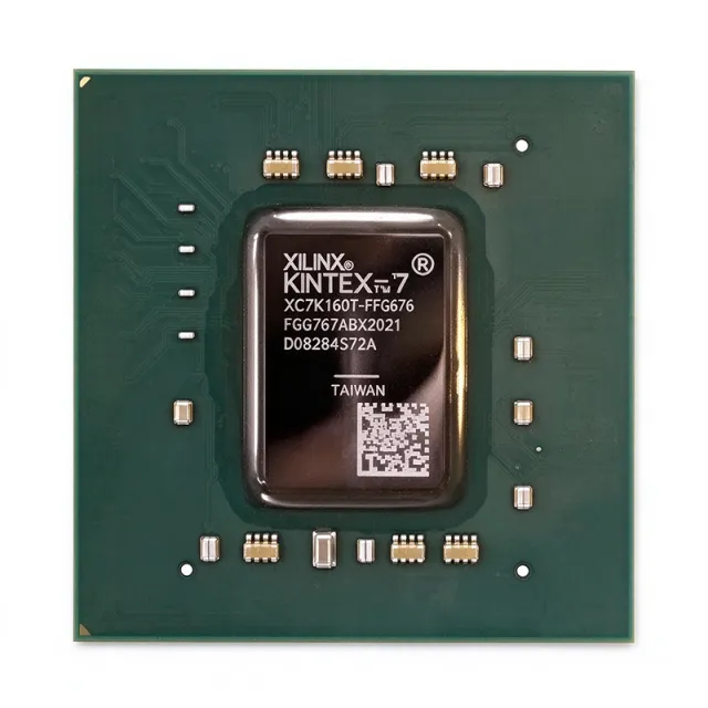
XCKU3P-1FFVB676I
XCKU3P-1FFVB676I - Kintex UltraScale+ FPGA | AMD
AMD XCKU3P-1FFVB676I is a Kintex UltraScale+ field-programmable gate array in a 676-pin FCBGA package. The device combines programmable logic, block RAM, DSP resources, high-speed serial connectivity, and general-purpose I/O in a single heterogeneous FPGA. Its XCKU3P designation identifies the high-performance Kintex UltraScale+ product family, while the -1 suffix identifies the -1 speed grade. The FFVB676 package designation identifies the 676-ball flip-chip BGA configuration used by this part.
A field-programmable gate array, or FPGA, is a semiconductor whose digital logic is configured after manufacture. FPGA architecture belongs to the broader programmable-logic hierarchy and can be classified as a semiconductor, integrated circuit, and digital logic device. Instead of implementing every digital function with fixed application-specific circuitry, an FPGA combines configurable logic blocks and dedicated hard resources with an interconnect fabric. This enables parallel processing, rapid hardware revision, and high integration in systems that require deterministic real-time behavior.
The XCKU3P family targets demanding communications, industrial, networking, signal-processing, and embedded-control systems. A Kintex UltraScale+ FPGA is useful when a design needs substantially more logic and serial throughput than lower-density programmable devices, while retaining a single-package implementation. The device combines a -1 performance grade with a large 676-pin package that provides extensive package I/O and power connectivity. Exact logic-cell, memory, DSP, I/O, and power specifications should be taken from the current AMD Kintex UltraScale+ data sheet for the selected package and speed grade.
Use the part in designs that benefit from parallel datapaths, hardware-assisted filtering, protocol termination, high-speed data movement, or adaptive control. Common engineering roles include accelerator logic, video and image processing, industrial control, test instrumentation, communications infrastructure, and high-speed interface bridging. AMD UltraScale+ devices use programmable logic, block RAM, DSP slices, high-speed I/O, and integrated power-management resources, allowing one device to implement control, datapath, and interface functions in parallel rather than requiring several discrete components.
The 676-ball FCBGA package is mechanically and electrically demanding. Board design must follow the AMD package pinout files and the device PCB-design guidance, including exact power and ground-plane connections, via arrays, decoupling placement, and ball-grid escape routing. Differential and high-speed interfaces require controlled impedance, careful return-path continuity, and compliance with the stated maximum transition-rate and board-routing constraints. Use the package-device pinout files from AMD when assigning every ball and when cross-checking the schematic, PCB library, and assembly drawings.
Thermal design is also central to FPGA implementation because logic utilization, I/O activity, and switching can increase dynamic power. The power budget should be calculated from the actual clocking, memory, DSP, serial-link, and I/O assumptions in the design, including worst-case activity factors. A conservative approach is to use the AMD power estimator and system-design guidance with the exact device, package, speed grade, and utilization. This page identifies the verified commercial configuration and the engineering constraints that should be checked before schematic release.
This product record combines the verified XCKU3P-1FFVB676I configuration, package information, related same-footprint variants, selection trade-offs, and practical implementation guidance. It is intended to help engineers identify the correct AMD/Xilinx Kintex UltraScale+ device and prepare a package-compliant, thermally valid, and production-ready FPGA design.
Permintaan RFG
Kontak