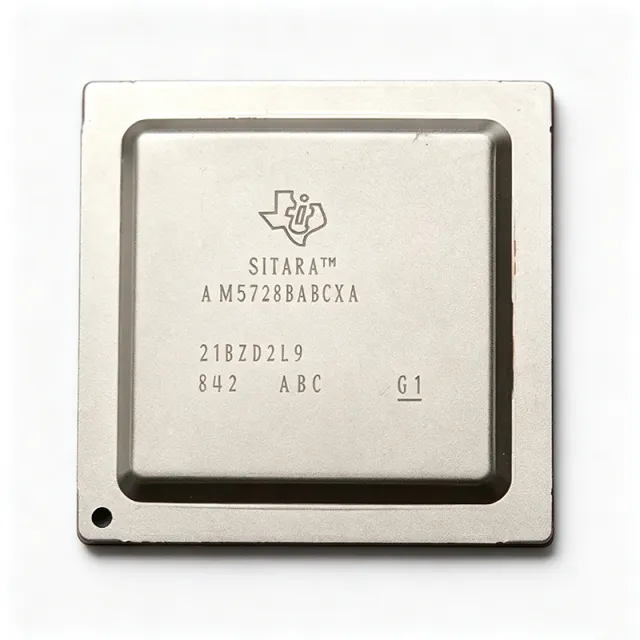
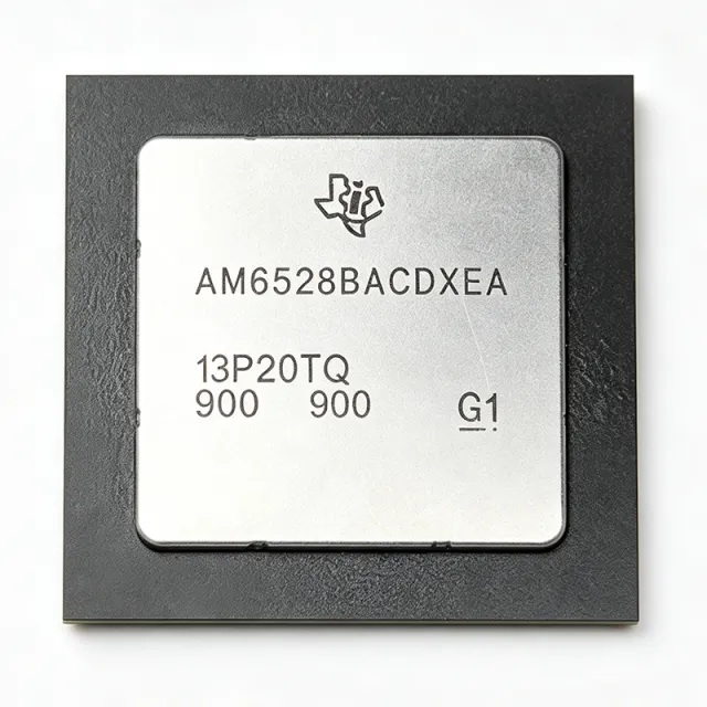
APA075-PQ208
APA075-PQ208 - 75K Gate Flash FPGA | Microchip Technology
The Microchip Technology APA075-PQ208 is a ProASICPLUS flash field-programmable gate array with 75,000 system gates, 3,072 logic cells, 158 user I/Os, and a maximum operating frequency of 180 MHz, packaged in a 208-lead BFQFP. The device combines reprogrammability and nonvolatile configuration with an ASIC-oriented development flow.
A field-programmable gate array is a programmable-logic semiconductor in which configurable logic blocks and interconnect resources implement digital functions after the device has been manufactured. In the application hierarchy, an FPGA belongs to programmable logic, CPLDs and FPGAs, digital integrated circuits, and semiconductors. The APA075 family is positioned as a low-density, flash-based alternative to mask-programmed ASIC development for prototypes, embedded control, interface logic, and general-purpose digital subsystems.
The ProASICPLUS architecture provides 75,000 system gates across 3,072 cells and 158 I/Os. Its nonvolatile flash configuration allows the programmed design to be retained when power is removed and supports live operation at power-up. A stated maximum frequency of 180 MHz provides a useful reference point for clocked designs, although actual operating frequency depends on the selected logic resources, routing paths, timing constraints, I/O standards, and system implementation.
This device uses a 208-lead quad flat package identified as 208-BFQFP in distributor records. The large pin count provides substantial board-level connectivity for parallel data buses, control interfaces, memory interfaces, and multi-clock digital subsystems. Its 158 user I/Os make it more suitable for parallel interface consolidation than low-pin-count FPGA or CPLD options, while the nonvolatile configuration supports repeatable field updates without separate configuration memories.
Typical uses include industrial control logic, data-acquisition systems, communications equipment, embedded instrumentation, and general-purpose interface bridging. In each case, the design can be programmed and revised during development, then deployed without changing the physical FPGA package or relying on an external volatile configuration device. The 180 MHz performance target also makes it appropriate for moderately timed control, status, and data-processing logic when timing closure is completed in the appropriate design tools.
PCB implementation should preserve the 208-BFQFP land pattern, power and ground distribution, clock integrity, and I/O signal routing specified by the manufacturer. Because this package has many leads, assembly and inspection require adequate solder-mask definition, pad geometry, and thermal management. The main design trade-off is the high pin count: it enables extensive I/O connectivity but requires a larger PCB footprint and more careful routing than compact low-pin-count programmable-logic packages.
This page combines the device identity, package, programming characteristics, verified alternatives, comparison rows, and practical integration considerations into a procurement-oriented engineering reference. It also highlights the principal selection issue: APA075-PQ208 should be chosen for flash-based, nonvolatile FPGA operation with a large 208-lead package, while any substitute must preserve both the land pattern and the timing, logic, and I/O requirements of the original design.
Permintaan RFG
Kontak