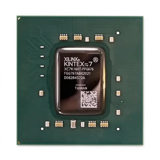
XCKU025-2FFVA1156E
XCKU025-2FFVA1156E - 318K Logic Cell FPGA | AMD
AMD XCKU025-2FFVA1156E is a Kintex UltraScale field-programmable gate array with 318,150 logic cells, 18,180 configurable logic blocks, 312 input/outputs, and a nominal 0.95 V core voltage. It is packaged in a 1156-ball FCBGA package for high-performance programmable logic, digital signal processing, and high-speed connectivity designs. The -2 speed grade, industrial temperature option, and extended-grade marking distinguish this configuration.
A field-programmable gate array is a semiconductor whose digital logic is configured after manufacture. FPGA devices sit within the broader programmable-logic hierarchy, combining configurable logic blocks, fixed or semi-hard DSP resources, block RAM, input/output resources, clocking, and programmable interconnect. Their advantage over fixed logic is rapid design iteration and adaptation, while their disadvantage compared with application-specific ASICs is generally higher unit cost and lower power efficiency.
The XCKU025 device provides 318,150 logic cells organized into 18,180 CLBs, creating substantial parallelism for control logic, protocol bridging, data acquisition, and high-throughput digital processing. Its 312 I/O resources support interfaces to external memory, clocks, serial transceivers, and board-level peripherals. The device also uses monolithic and advanced stacked-silicon interconnect technology, connecting an unusually large programmable fabric with dedicated resources and next-generation transceivers.
The 0.95 V nominal core voltage identifies this as a high-performance FPGA platform intended for demanding signal-processing and connectivity applications. Available architecture features should be assigned through the Vivado Design Suite, which provides device-aware synthesis, implementation, timing analysis, and programming support. Designers must also use the AMD UltraScale package-device pinout files when assigning balls and PCB constraints for the 1156-ball FCBGA footprint.
Typical uses include high-speed data acquisition, industrial control, test and measurement, networking, embedded vision, signal processing, and communications infrastructure. In each case, the large logic-cell count supports parallel algorithms, while the 312 available I/Os and high-speed transceivers provide connectivity between the FPGA fabric, memory, and external interfaces. The 1156-ball package demands careful power delivery, decoupling, thermal planning, and high-density PCB layout execution.
A critical design consideration is that the speed grade, temperature grade, package suffix, and device marking must all match the intended production environment. Programming files and bitstream compatibility must be checked against the exact device identifier before manufacturing. Because this is a large BGA device, assembly yield, via-in-pad construction, solder-paste control, and X-ray inspection quality can materially affect production cost.
This page combines the exact device identity, pinout-resource location, package information, engineering selection criteria, and same-footprint replacement guidance. It also distinguishes direct configuration alternatives from broader FPGA options, helping engineers evaluate performance grade, temperature range, lifecycle requirements, and board compatibility before requesting a quotation.
Permintaan RFG
Kontak