STM32F767NIH7
STM32F767NIH7 - 216MHz Cortex-M7 2MB MCU | STMicroelectronics
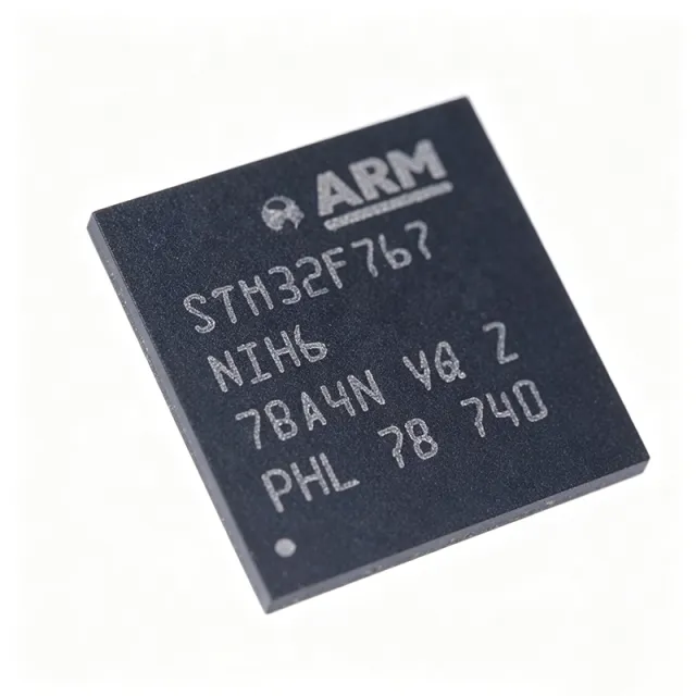
STMicroelectronics STM32F767NIH7 is an Arm Cortex-M7 32-bit microcontroller with a 216 MHz maximum operating frequency, 2 MB of embedded Flash memory, and a 216-pin TFBGA package measuring 13 mm by 13 mm. It also provides a floating-point unit, 462 DMIPS, DSP instructions, an MPU, and separate 16 KB instruction and data caches. The MCU is designed for high-performance embedded control, data acquisition, communications, and applications requiring substantial local memory.
A microcontroller is a programmable semiconductor that integrates a processor core, memory, peripherals, and communication interfaces on one device. In the embedded-device hierarchy, the STM32F767NIH7 belongs to the 32-bit Arm Cortex-M7 microcontroller class, combining real-time control capability with high-throughput digital signal processing. Its 2 MB Flash stores firmware and constants, while its SRAM supports working data, stack operations, DMA buffers, graphics data, and communication frames.
Key features include operation up to 216 MHz, a 462 DMIPS processing rating, and a dedicated floating-point unit for mathematically intensive control and signal-processing tasks. The Cortex-M7 core supports DSP instructions, zero-wait-state execution from embedded Flash through the stated cache architecture, and an MPU for memory protection. Verified sources also identify USB OTG high-speed and full-speed operation, up to 28 communication interfaces, LCD and DSI support, and a broad collection of analog and timer peripherals.
The device architecture combines a high-performance 32-bit RISC core with extensive connectivity. Its 16 KB instruction cache and 16 KB data cache help reduce memory-access penalties, while the ART Accelerator supports embedded-Flash execution according to the manufacturer datasheet. Total SRAM is listed as 512 KB, 16 KB, and 4 KB in separate memory regions, allowing firmware designers to partition code, data, and communications or display buffers without relying entirely on external memory.
Typical applications include industrial data-acquisition and factory-control equipment, connected embedded systems requiring USB, high-speed graphical or camera interfaces, and real-time signal-processing systems. The 216 MHz core and FPU benefit filtering, control algorithms, and protocol handling, while the 2 MB Flash accommodates larger firmware images and richer user interfaces. The 216-pin TFBGA also provides access to the family's extensive GPIO and peripheral set but requires careful escape routing and multilayer PCB design.
Designers should base the PCB footprint and pin assignments on the manufacturer package drawing rather than generic BGA conventions. The 13 mm by 13 mm TFBGA requires a dense, controlled fanout, thermal management appropriate for the selected power dissipation, and verification of signal integrity on high-speed interfaces. Firmware should also account for peripheral errata, clock-tree configuration, memory placement, and independent USB, Ethernet, display, and DMA requirements before production release.
This page consolidates the verified manufacturer specifications, distributor package information, comparison parameters, and application guidance for STM32F767NIH7. It also distinguishes directly compatible STM32F7 package options from cross-brand alternatives, helping engineering teams choose a replacement while preserving PCB, firmware, qualification, and procurement requirements.
Permintaan RFG
Kontak