XC7A100T-L2CSG324E vs XC7A100T-2CSG324C Perbandingan
Perbandingan bersamaan detil XC7A100T-L2CSG324E dari AMD dan XC7A100T-2CSG324C dari AMD. Bandingkan spesifikasi penting, parameter listrik, pengemasan, status cycle, harga, dan ketersediaan untuk menentukan komponen terbaik untuk kebutuhan desain Anda.

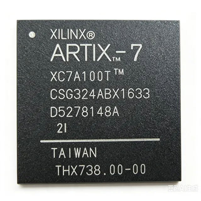
Perbandingan Spesifikasi
| Parameter Umum | XC7A100T-L2CSG324E | XC7A100T-2CSG324C |
|---|---|---|
| Merek | AMD | AMD |
| Kategori | FPGA & CPLD | FPGA & CPLD |
| Status Lingkungan Hidup | Aktif | Aktif |
| Harga Unit (USD) | — | $59,50 |
| FPGA Family | Artix-7 | — |
| Logic Cells | 101,440 cells | 101440 |
| Block RAM | 4,860 Kb | 4860 Kb |
| DSP Slices | 240 slices | 240 |
| Process Technology | 28 nm | — |
| Operating Voltage Class | 1 V | — |
| Paket | 324-terminal FC-BGA (CSG324) | CSBGA-324 (CSG324) |
| Terminal Count | 324 terminals | — |
| Temperature Grade | Extended, E grade | — |
| Junction Temperature Range | 0°C to 100°C | — |
| Speed Grade | -L2 | -2 |
| Tipe Mounting | Surface mount | — |
| Programmable Logic Type | FPGA | — |
| On-Chip RAM | 4,860 Kb block RAM | — |
| Digital Signal Processing | 240 DSP slices | — |
| Configuration Memory | [DATA_NEEDED: configuration memory type and capacity] | — |
| Maximum I/O Count | [DATA_NEEDED: maximum user I/O count] | — |
| RoHS Compliance | [DATA_NEEDED: RoHS compliance status] | — |
| Family | — | Artix-7 |
| User I/O | — | 210 |
| Core Voltage | — | 1.0 V |
| I/O Voltage | — | 1.2V to 3.3V |
| Suhu Kerja | — | 0C to +85C |
| Clock Management Tiles | — | 6 |
| PCIe Blocks | — | 1 (Gen2 x1) |
| Gigabit Transceivers | — | 4 (up to 6.6 Gbps) |
| Configuration | — | SRAM-based, supports SPI, BPI, JTAG |
| Status RoHS | — | Compliant |