XC7K325T-2FFG900I vs XC7K325T-1FFG900CES Perbandingan
Perbandingan bersamaan detil XC7K325T-2FFG900I dari AMD dan XC7K325T-1FFG900CES dari AMD. Bandingkan spesifikasi penting, parameter listrik, pengemasan, status cycle, harga, dan ketersediaan untuk menentukan komponen terbaik untuk kebutuhan desain Anda.
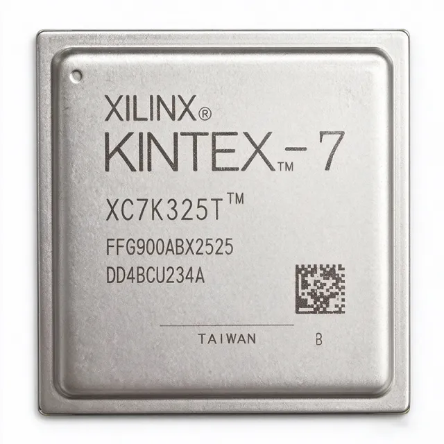

Perbandingan Spesifikasi
| Parameter Umum | XC7K325T-2FFG900I | XC7K325T-1FFG900CES |
|---|---|---|
| Merek | AMD | AMD |
| Kategori | FPGA & CPLD | FPGA & CPLD |
| Status Lingkungan Hidup | Aktif | Aktif |
| Status Stok | In Stock | — |
| Harga Unit (USD) | $65,00 | — |
| Family | Kintex-7 | — |
| Logic Cells | 326080 | — |
| Block RAM | 16404480 bits | — |
| DSP Slices | 840 | — |
| User I/O | 500 | 500 I/O |
| Paket | 900-BBGA, FCBGA | 900-BBGA FCBGA, FFG900 |
| Speed Grade | -2 | -1 |
| Temperature Grade | Industrial (-40°C to +100°C) | — |
| Process Technology | 28nm | — |
| Core Voltage (VCCINT) | 1.0V | — |
| I/O Standards | LVCMOS, LVDS, HSTL, SSTL | — |
| Transceivers | 16 (GTX) | — |
| PCIe Support | Gen3 | — |
| Status RoHS | Compliant | — |
| Tipe Mounting | Surface Mount | Surface mount |
| Device Type | — | Kintex-7 Field Programmable Gate Array (FPGA) |
| Programmable Logic Cells | — | 326080 cells |
| Configurable Logic Blocks | — | 25475 CLBs |
| Internal Memory | — | 16404480 bits |
| Maximum Clock Figure | — | 1098 MHz |
| High-Speed Transceivers | — | 16 transceivers |
| Ball Count | — | 900 balls |
| Programmable Logic Type | — | CMOS FPGA |
| Series | — | Kintex-7 |
| Configuration | — | FPGA configuration bitstream |
| Logic Resources | — | Programmable logic, block RAM, DSP, I/O, clocking, and GTX transceiver resources |
| Package Pinout Reference | — | Kintex-7 package device pinout files and UG475 |
| Operating Voltage | — | [DATA_NEEDED: core and I/O operating voltage] |
| Rentang Suhu Kerja | — | [DATA_NEEDED: ES suffix temperature range] |
| I/O Standard | — | [DATA_NEEDED: supported I/O standards] |
| RoHS Compliance | — | unknown |
| REACH Compliance | — | unknown |