XCKU035-1FBVA676C vs XCKU035-3FBVA676E Perbandingan
Perbandingan bersamaan detil XCKU035-1FBVA676C dari AMD dan XCKU035-3FBVA676E dari AMD. Bandingkan spesifikasi penting, parameter listrik, pengemasan, status cycle, harga, dan ketersediaan untuk menentukan komponen terbaik untuk kebutuhan desain Anda.
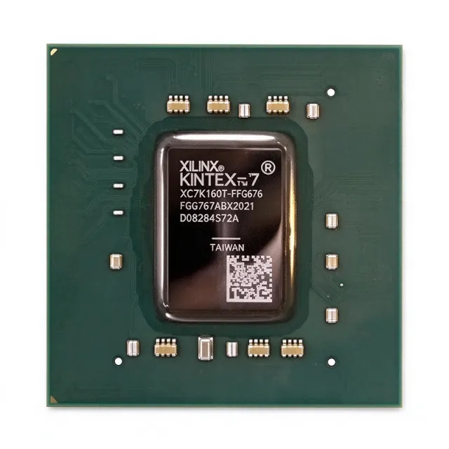

Perbandingan Spesifikasi
| Parameter Umum | XCKU035-1FBVA676C | XCKU035-3FBVA676E |
|---|---|---|
| Merek | AMD | AMD |
| Kategori | FPGA & CPLD | FPGA & CPLD |
| Status Lingkungan Hidup | Aktif | Aktif |
| Status Stok | In Stock | — |
| Harga Unit (USD) | $467,66 | — |
| Family | Kintex UltraScale | — |
| Process Node | 20 nm TSMC planar CMOS | — |
| Logic Cells | 444,343 | — |
| System Gates | 19,456,000 | — |
| Speed Grade | -1 | -3 |
| Maximum Fabric Frequency | 630 MHz | — |
| Paket | 676-ball FCBGA (FBVA676), 27 mm × 27 mm | — |
| User I/Os | 312 | — |
| DSP48E2 Slices | 240 | — |
| Block RAM | 2,160 Kb (540 × 36 Kb blocks) [DATA_NEEDED: distributed RAM total] | — |
| Distributed RAM | 4.7 Mb | — |
| MMCM / PLL | 3 MMCM, 8 PLL | — |
| GTH Transceivers | 16 (12.5 Gb/s) [DATA_NEEDED: confirm for integrated XCKU035 part] | — |
| Memory Interface Support | DDR4 up to 1,250 Mbps | — |
| PCIe Hard Cores | 1 × PCIe Gen3 x8 [DATA_NEEDED: confirm lane count for integrated XCKU035 part] | — |
| Core Voltage (VCCINT) | 0.95 V | — |
| Temperature Grade (suffix C) | 0 °C to +85 °C (Commercial) | — |
| Tipe Mounting | Surface Mount, BGA | Surface mount |
| Status RoHS | Compliant | [DATA_NEEDED: RoHS status] |
| Device Type | — | Kintex UltraScale field-programmable gate array |
| Programmable Logic Cells | — | 444343 cells |
| Listed Programmable Resources | — | 19456000 |
| Listed Package Entries | — | 312 |
| Performance Class | — | Highest-performance Kintex UltraScale speed grade |
| FPGA Process Technology | — | 20 nm |
| Package Type | — | 676-BBGA FCBGA |
| Package Ball Count | — | 676 balls |
| Logic Architecture | — | Configurable digital logic fabric |
| Programmable Resources | — | 444343-cell Kintex UltraScale FPGA |
| Configuration Interface | — | [DATA_NEEDED: Configuration interface details] |
| Operating Voltage | — | [DATA_NEEDED: VCCINT and auxiliary supply voltages] |
| Rentang Suhu Kerja | — | [DATA_NEEDED: Exact operating temperature range for the E suffix] |
| I/O Standard | — | [DATA_NEEDED: Supported I/O standards] |
| Maximum I/O Performance | — | [DATA_NEEDED: Maximum I/O data rate] |
| Transceiver Count | — | [DATA_NEEDED: Transceiver count] |
| DSP Block Count | — | [DATA_NEEDED: DSP block count] |
| Block RAM Capacity | — | [DATA_NEEDED: Block RAM capacity] |