XCKU5P-2FFVB676I vs XCKU5P-1FFVB676I Perbandingan
Perbandingan bersamaan detil XCKU5P-2FFVB676I dari AMD dan XCKU5P-1FFVB676I dari AMD. Bandingkan spesifikasi penting, parameter listrik, pengemasan, status cycle, harga, dan ketersediaan untuk menentukan komponen terbaik untuk kebutuhan desain Anda.
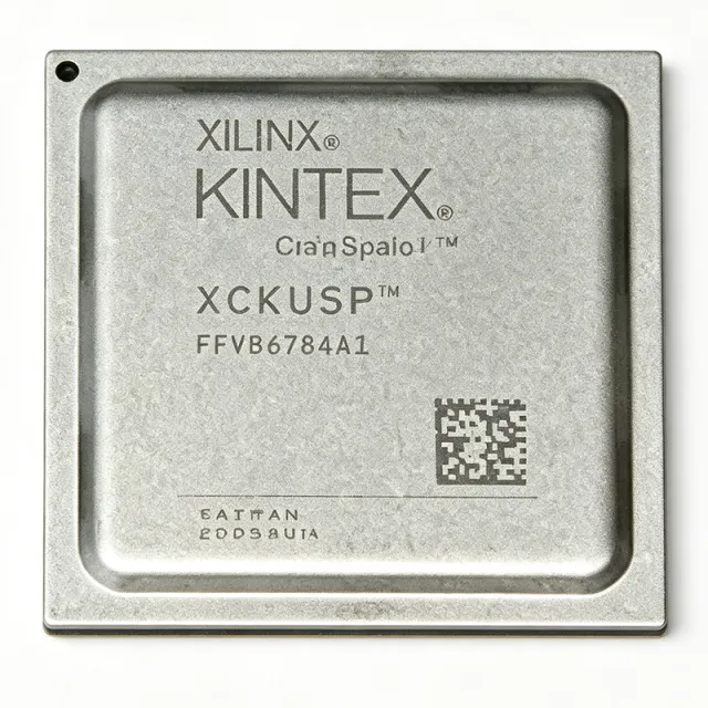

Perbandingan Spesifikasi
| Parameter Umum | XCKU5P-2FFVB676I | XCKU5P-1FFVB676I |
|---|---|---|
| Merek | AMD | AMD |
| Kategori | FPGA & CPLD | FPGA & CPLD |
| Status Lingkungan Hidup | Aktif | Aktif |
| Harga Unit (USD) | $1.660,00 | — |
| Family | Kintex UltraScale+ | — |
| Logic Cells | 474600 | 474,600 cells |
| System Logic Cells | 474600 | — |
| Block RAM | 41984000 bits | 41,984,000 bits |
| User I/O | 280 | — |
| Maximum Internal Clock Frequency | 725 MHz | — |
| Core Supply Voltage | 825 mV to 876 mV | — |
| Speed Grade | -2 | -1 |
| Clock Management | MMCM, PLL | — |
| Process Technology | 16 nm FinFET | 16 nm FinFET+ |
| Paket | 676-BBGA, FCBGA (FFVB676) | 676-ball FCBGA |
| Terminal Form | Ball | — |
| Tipe Mounting | Surface Mount | — |
| Suhu Kerja | -40C to +100C (Industrial) | — |
| Temperature Grading | Industrial (I) | — |
| Status RoHS | Compliant | [DATA_NEEDED: RoHS compliance status] |
| Device Type | — | Kintex UltraScale+ FPGA |
| Configurable Logic Blocks | — | 27,120 CLBs |
| User I/Os | — | 280 I/Os |
| DSP Slices | — | 1,824 DSP slices |
| High-Speed Transceivers | — | 16 GTY transceivers |
| Maximum Transceiver Data Rate | — | 32.75 Gb/s per transceiver |
| Maximum Operating Frequency | — | 630 MHz |
| Core Voltage Range | — | 825 mV to 876 mV |
| Package Dimensions | — | 27 mm x 27 mm |
| Clocking Features | — | MMCM and PLL |
| Rentang Suhu Kerja | — | [DATA_NEEDED: operating temperature range] |
| Supply Voltage Tolerance | — | [DATA_NEEDED: supply voltage tolerance] |