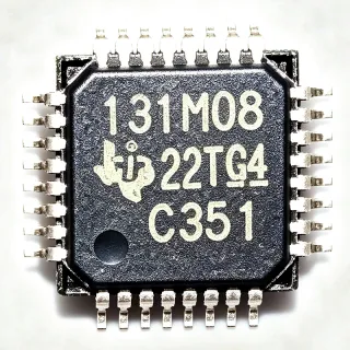
ADS8322YB/2KG4 - 16-Bit 500kSPS SAR ADC, 32-TQFP | Texas Instruments
MPN: ADS8322YB/2KG4 ✗ Akhir HidupADS8322YB/2KG4 Ringkasan
A SAR ADC is a type of analog-to-digital converter that uses a binary search algorithm against an internal precision DAC to determine each bit sequentially within one conversion cycle. SAR ADCs sit in the signal chain between the analog front end (sensor, amplifier, anti-alias filter) and the digital controller (FPGA, MCU, DSP); they offer deterministic latency, no pipeline delay, and inherently good DC accuracy - making them the converter class of choice for multiplexed data acquisition, industrial control loops, and precision instrumentation.
Key features of the ADS8322YB/2KG4 include a 16-bit capacitor-based SAR core with inherent sample-and-hold, an integrated 2.5V reference (eliminating an external reference IC and saving BOM cost), low power consumption at 500 kSPS throughput, and a parallel interface that supports either 16-bit or 8-bit bus mode. The /2K suffix indicates tape-and-reel packaging, while G4 denotes a Pb-free (lead-free) finish.
Architecturally, the device combines a charge-redistribution DAC, a precision internal bandgap reference, and a successive-approximation register. The single 5V supply simplifies system power, and the high-speed parallel interface allows direct connection to FPGAs and DSPs without glue logic. Compared with pipelined ADCs of similar speed, the ADS8322 delivers better DC linearity for multiplexed-channel scanning because there is no pipeline latency to flush between conversions.
Typical applications include data acquisition systems, industrial process control, optical networking power monitoring, portable instrumentation, and battery-powered test equipment. Designers also use the part in precision weigh scales, medical patient monitoring front ends, and motor-control feedback loops.
When designing with the ADS8322YB/2KG4, ensure the analog input is driven by a low-impedance buffer with sufficient bandwidth to settle within the acquisition window, and use a clean 5V analog supply well decoupled at the AVdd pin. The /2K G4 ordering code identifies lead-free tape-and-reel packaging.
This page synthesizes distributor pricing, drop-in alternatives, and practical design notes not found in the manufacturer datasheet.
Alternatif penggantian untuk ADS8322YB/2KG4 — paket yang sama, pin-pada-pin kompatibel. Bagian paket yang berbeda memerlukan kerja ulang PCB diabaikan.
ADS8322YB/250
✅ Drop-In📋 Alternatif referensi (tidak dalam katalog)
ADS8322YB/2K
✅ Drop-In📋 Alternatif referensi (tidak dalam katalog)
ADS8322YB
✅ Drop-In ⚠️ Spesifikasi Tidak Disahkan📋 Alternatif referensi (tidak dalam katalog)
ADS8322E/2K
✅ Drop-In ⚠️ Spesifikasi Tidak Disahkan📋 Alternatif referensi (tidak dalam katalog)
ADS8323
✅ Drop-In ⚠️ Spesifikasi Tidak Disahkan📋 Alternatif referensi (tidak dalam katalog)
ADS8322YB/2KG4 Rating Maksimal & Karakteristik Listrik
| Resolusi | 16 bit |
| Laju Pengambilan Sampel | 500 kSPS |
| Converter Type | SAR (Successive Approximation Register) |
| Number of Input Channels | 1 |
| Input Range | Unipolar |
| Internal Reference Voltage | 2.5 V |
| Tegangan Pemuat | 5 V (single supply) |
| Data Interface | Parallel (16-bit or 8-bit mode) |
| Conversion Time | 1.6 us (typ) |
| Linearity Error (DNL/INL) | 0.0092% |
| Paket | 32-TQFP (5x5 mm) |
| Package Code | TFQFP (TQFP-32, gull wing) |
| Temperature Grade | Industrial |
| Status RoHS | Pb-free (lead-free) per G4 suffix |
Konfigurasi Pin ADS8322YB/2KG4
| Pin produk 1 | AVDD — Analog supply voltage (5 V) |
| Pin produk 2 | AGND — Analog ground |
| Pin produk 3 | IN+ — Analog input (positive) |
| Pin produk 4 | IN- — Analog input (negative, normally tied to AGND for unipolar) |
| Pin produk 5 | REF — Reference decoupling pin (internal 2.5 V reference) |
| Pin produk 6 | AGND — Analog ground |
| Pin produk 7 | AVDD — Analog supply voltage (5 V) |
| Pin produk 8 | DGND — Digital ground |
| Pin produk 9 | BYTE — Bus-width select (16-bit or 8-bit mode) |
| Pin produk 10 | CS — Chip select (active low) |
| Pin produk 11 | RD — Read strobe (active low) |
| Pin produk 12 | CONVST — Conversion start input |
| Pin produk 13 | EOC/INT — End-of-conversion / interrupt output |
| Pin produk 14 | DVDD — Digital supply voltage (5 V) |
| Pin produk 15 | DB15 — Data bit 15 (MSB) |
| Pin produk 16 | DB14 — Data bit 14 |
| Pin produk 17 | DB13 — Data bit 13 |
| Pin produk 18 | DB12 — Data bit 12 |
| Pin produk 19 | DB11 — Data bit 11 |
| Pin produk 20 | DB10 — Data bit 10 |
| Pin produk 21 | DB9 — Data bit 9 |
| Pin produk 22 | DB8 — Data bit 8 |
| Pin produk 23 | DB7 — Data bit 7 |
| Pin produk 24 | DB6 — Data bit 6 |
| Pin produk 25 | DB5 — Data bit 5 |
| Pin produk 26 | DB4 — Data bit 4 |
| Pin produk 27 | DB3 — Data bit 3 |
| Pin produk 28 | DB2 — Data bit 2 |
| Pin produk 29 | DB1 — Data bit 1 |
| Pin produk 30 | DB0 — Data bit 0 (LSB) |
| Pin produk 31 | DGND — Digital ground |
| Pin produk 32 | DVDD — Digital supply voltage (5 V) |
Aplikasi Umum
ADS8322YB/2KG4 cocok untuk 6 aplikasis: Industrial Data Acquisition Systems, Optical Networking Power Monitoring, Portable Instrumentation and Test Equipment, Precision Weigh Scales, Motor Control Feedback Loops, Medical Patient Monitoring Front End.
Industrial Data Acquisition Systems
The ADS8322YB/2KG4 fits 16-bit multiplexed data acquisition front ends because its 500 kSPS SAR throughput and deterministic single-cycle latency allow rapid scanning of sensor channels without the pipeline delay of pipelined ADCs. The internal 2.5 V reference removes one BOM line and improves long-term gain stability in calibration loops. Use it between the analog front end (sensor + buffer + anti-alias filter) and an FPGA or MCU back end; the parallel 16-bit interface drops straight into standard 16-bit DSP or FPGA data buses.
Direkomendasikan
Optical Networking Power Monitoring
In optical line cards and transponder modules the ADS8322YB/2KG4 monitors photodiode current via a transimpedance amplifier feeding its 0 V to 2.5 V unipolar input. The 500 kSPS rate captures fast AGC settling events, while the parallel 16-bit interface pairs naturally with the FPGA on the line card. Low power at 500 kSPS helps stay within the tight power budget of multi-port dense wavelength-division multiplexing (DWDM) modules.
Direkomendasikan
Portable Instrumentation and Test Equipment
Handheld multimeters, oscilloscope front ends, and laboratory data loggers benefit from the ADS8322YB/2KG4's integrated 2.5 V reference, low power at 500 kSPS, and parallel read that simplifies timing in microcontroller-based designs. The 32-TQFP footprint enables compact PCB layouts in portable enclosures, and the SAR architecture gives one-conversion deterministic latency ideal for triggered single-shot measurements.
Direkomendasikan
Precision Weigh Scales
The ADS8322YB/2KG4 drives precision weigh scale signal chains where load-cell output is amplified to the 0 V to 2.5 V range and digitized directly. The 16-bit resolution and low integral nonlinearity support high-resolution weight readings, while the SAR topology's lack of pipeline delay produces stable readings right after the load is applied. The internal reference simplifies factory calibration and reduces long-term drift.
Direkomendasikan
Motor Control Feedback Loops
In brushless DC and servo motor drives the ADS8322YB/2KG4 samples current-sense amplifier output to close the FOC current loop. The 500 kSPS rate is sufficient for several-microsecond current-loop update times, and the SAR's single-cycle latency eliminates the pipeline delay that complicates control law timing in pipelined converters. Place it on the same 5 V analog rail that powers the gate drivers for a clean, isolated feedback path.
Direkomendasikan
Medical Patient Monitoring Front End
Patient monitors digitize ECG, SpO2, and temperature signals with the ADS8322YB/2KG4 in a precision 16-bit SAR configuration. The deterministic latency and parallel 16-bit interface simplify the timing logic in DSP-based monitor designs, while the low power dissipation helps meet IEC 60601-1 patient-leakage budgets when the monitor is battery powered. Use a low-noise LDO on the 5 V analog rail to preserve the ADC's noise floor.
Direkomendasikan
Ringkasan Produk Direkomendasikan
Data referensi engineering untuk ADS8322YB/2KG4 — pembandingan, panduan desain, dan informasi konformitas.
Panduan Pemilihan
Pembandingan dengan Alternatif
| Parameter Umum | Produk Ini | ADS8322YB/250 | ADS8322YB/2K | ADS8322YB | ADS8322E/2K | ADS8323 |
|---|---|---|---|---|---|---|
| Package | 32-TQFP (5x5 mm) | 32-TQFP (5x5) - same | 32-TQFP (5x5) - same | 32-TQFP (5x5) - same | 32-TQFP (5x5) - same | 32-TQFP (5x5) - same |
| Brand | Texas Instruments | Texas Instruments | Texas Instruments | Texas Instruments | Texas Instruments | Texas Instruments |
| Resolution | 16 bit | 16 bit | 16 bit | 16 bit | 16 bit | 16 bit |
| Internal Reference | 2.5 V (internal) | 2.5 V (internal) | 2.5 V (internal) | 2.5 V (internal) | 2.5 V (internal) | 2.5 V (internal) |
| Input Range | Unipolar | Unipolar | Unipolar | Unipolar | Unipolar | Unipolar |
| Data Interface | Parallel (16/8-bit) | Parallel (16/8-bit) | Parallel (16/8-bit) | Parallel (16/8-bit) | Parallel (16/8-bit) | Parallel |
| Lifecycle Status (2026-10-13) | Obsolete | Active | Active | Active | Active | Active |
Diferensiator Kunci
- Integrated 2.5 V reference on-chip (vsADS8322YB/250)
- SAR architecture with deterministic single-cycle latency (vsPipelined ADCs (e.g. AD9226))
- Parallel 16-bit or 8-bit multiplexed bus (vsADS8322E/2K (extended temperature grade))
Catatan Desain
Estimated: power dissipation at 5 V AVDD and 500 kSPS continuous conversion is approximately 5 V x I_AVDD. Per the TI ADS8322 datasheet the analog supply current scales linearly with sampling rate; place a 10 uF tantalum plus 0.1 uF ceramic decoupling pair directly at the AVDD and DVDD pins. Power AVDD from a low-noise LDO (e.g. TPS7A4701) to preserve the SAR's noise floor, and keep the analog and digital 5 V rails star-grounded at the ADC.
Route analog input traces as a guarded differential pair from the buffer output directly to IN+ and IN-, with AGND guard traces on both sides to reject switching noise from the parallel digital bus. Keep the parallel data bus (DB0-DB15, CS, RD, CONVST, EOC) tightly bunched and series-terminated near the digital side, with a ground island separating the analog input pins from the digital bus on the top layer. Place the reference decoupling capacitor (typically 4.7 uF) directly at the REF pin to filter internal reference noise.
The SAR conversion requires the analog input to settle within the acquisition window (typically less than 500 ns at 500 kSPS); drive IN+ through a low-impedance, wide-bandwidth op-amp buffer such as the OPA2227 or THS4032. Verify with a scope that the input settles to within 1 LSB (152 uV for 2.5 V reference) before CONVST rising edge, otherwise DNL/INL errors will appear in the conversion result.
Common pitfalls with the ADS8322YB/2KG4 include: (1) leaving the BYTE pin floating - tie BYTE high for 8-bit mode or low for full 16-bit mode; (2) cross-coupling between IN- and ground - tie IN- to AGND at the IC pin, not at the source; (3) using a single AVDD/DVDD supply without separate filtering - the parallel digital switching can couple noise into AVDD. Also note the /2KG4 suffix is obsolete as of 2026-10-13, so secure last-time-buy inventory before design-in.
Informasi Konformitas
G4 suffix per TI ordering code indicates Pb-free (lead-free) finish. RoHS and REACH compliant per TI product page; AEC-Q100 not qualified - choose automotive-grade alternatives for vehicle applications.