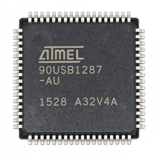
ATXMEGA256D3-AU - 32MHz 256KB Flash AVR MCU | Microchip
MPN: ATXMEGA256D3-AU ✓ AktifATXMEGA256D3-AU Ringkasan
An 8/16-bit microcontroller is a compact embedded-processing device that executes instructions from internal Flash memory while using dedicated peripherals to interact with sensors, communication circuits, and actuators. Within the component hierarchy, the ATXMEGA256D3-AU is an AVR XMEGA microcontroller, an enhanced RISC processor family designed to combine deterministic control, event-driven hardware handling, and low-power operation in a single device.
The XMEGA D3 feature set includes a four-channel event system, a programmable multi-level interrupt controller, a 16-bit real-time counter, and five flexible 16-bit timer/counter blocks with compare modes and PWM support. These resources allow software to offload periodic timing, edge detection, and signal routing to dedicated hardware, reducing interrupt-handling overhead in motor, lighting, and industrial control systems.
The device operates from a 2.7 V to 3.6 V supply and reaches a maximum clock rate of 32 MHz. Its memory architecture is organized for embedded firmware and parameter storage: 256 KB of Flash holds application code and the 8 KB boot section, 4 KB of EEPROM preserves configuration values across power cycles, and 16 KB of SRAM supports stack, buffers, and real-time state. The 34-port figure reported for the device reflects the usable port resources associated with the 50 general-purpose I/O lines and package implementation.
Typical applications include industrial automation modules, data loggers, motor and pump controllers, LED lighting systems, USB-connected peripherals, and compact sensor-hub products. The 50 I/O lines permit multiple digital interfaces to coexist on one board, while the event system and five timer/counter blocks support deterministic periodic control without excessive firmware polling.
When laying out a board, route the clock, programming interface, and sensitive analog inputs according to the pin-description table in the manufacturer datasheet. Decoupling requirements and external component recommendations should also follow that document. Confirm the operating voltage, clock source, programming method, and boot configuration before releasing a PCB layout, because incorrect peripheral multiplexing or startup settings can prevent a fully populated board from operating as intended.
This page combines the manufacturer's XMEGA D3 specifications with a package-focused comparison, practical design guidance, drop-in candidate evaluation, and application-specific engineering context. It is intended to accelerate component selection and board planning beyond the basic distributor specification table.
Alternatif penggantian untuk ATXMEGA256D3-AU — paket yang sama, pin-pada-pin kompatibel. Bagian paket yang berbeda memerlukan kerja ulang PCB diabaikan.
ATXMEGA256D3-MH
✅ Drop-In📋 Alternatif referensi (tidak dalam katalog)
ATXMEGA256D3-MNR
✅ Drop-In📋 Alternatif referensi (tidak dalam katalog)
ATXMEGA128A4U-AN
✅ Drop-In📋 Alternatif referensi (tidak dalam katalog)
ATXMEGA128C3-AN
✅ Drop-In📋 Alternatif referensi (tidak dalam katalog)
ATXMEGA256D3-AU Rating Maksimal & Karakteristik Listrik
| Product Type | 8/16-bit AVR XMEGA D3 microcontroller |
| Maximum Clock Speed | 32 MHz |
| Flash Memory | 256 KB (128K x 16) |
| Boot Code Section | 8 KB |
| EEPROM | 4 KB |
| SRAM | 16 KB |
| General-Purpose I/O Lines | 50 |
| I/O Port Count | 34 |
| Event System | 4 channels |
| Interrupt Controller | Programmable multi-level |
| Real-Time Counter | 16-bit |
| Timer/Counter Blocks | 5 flexible 16-bit blocks with compare modes and PWM |
| Supply Voltage Range | 2.7 V to 3.6 V |
| Paket | 64-TQFP, 14 x 14 mm |
| Tipe Mounting | Surface mount |
| Program Memory Type | ISP Flash with read-while-write capability |
| Status Lingkungan Hidup | Active |
ATXMEGA256D3-AU 64-tqfp, 14 x 14 mm Diamant Konfigurasi Panduan
Konfigurasi pin untuk ATXMEGA256D3-AU (64-tqfp, 14 x 14 mm pakai pakai). IC digital ini termasuk GPIO, antarmuka komunikasi (UART, SPI, I2C), dan pin kuasa. Lihat datasheet produsen untuk fungsi pin alternatif dan opsi konfigurasi. Penting untuk desain sistem pengemasan dan PCB.

Tidak ada data diatribut pin yang tersedia untuk ATXMEGA256D3-AU.
Lihat ke: datasheet produk untuk konfigurasi pin penuh.
Aplikasi Umum
ATXMEGA256D3-AU cocok untuk 6 aplikasis: Industrial Automation Controller, Three-Phase Motor and Pump Control, USB Connected Data Logger, LED Lighting and Dimming Controller, Battery-Powered Sensor Hub, Security and Access-Control Panel.
Industrial Automation Controller
The ATXMEGA256D3-AU fits compact industrial automation modules that coordinate sensors, digital actuators, and field-bus transceivers. Its 50 general-purpose I/O lines provide ample routing for limit switches, status indicators, interlocks, and isolated interface signals, while the five 16-bit timer/counter blocks support periodic sampling and output timing. The 256 KB Flash provides room for protocol stacks, diagnostics, and field-upgrade logic. The device's four-channel event system can route external events directly to peripherals, reducing firmware polling and improving response time. Firmware should still reserve bootloader space, validate the 2.7 V to 3.6 V supply during transitions, and isolate external signals according to the system's noise environment.
Direkomendasikan
Three-Phase Motor and Pump Control
The ATXMEGA256D3-AU is appropriate for brushless motor, pump, and actuator controllers requiring precise PWM generation and multiple timing inputs. Five 16-bit timer/counter blocks with compare modes can produce PWM and capture input edges, while the 16-bit real-time counter supports long-duration scheduling. Fifty I/O lines leave room for gate-driver signals, hall-effect sensors, fault inputs, and an encoder interface. Firmware can use the event system to link sensor changes to timer actions, reducing interrupt latency. Confirm timer-clock limits, dead-time implementation, PWM frequency, and overcurrent response in the manufacturer datasheet before driving a power stage.
Direkomendasikan
USB Connected Data Logger
The ATXMEGA256D3-AU can serve as the control hub in a USB-connected data logger or configuration device. Its 256 KB of ISP Flash stores firmware, logging formats, and parameter sets, while 16 KB of SRAM supports working buffers and protocol state. Read-while-write Flash capability and the 8 KB boot-code section enable controlled field updates, and 4 KB of EEPROM retains calibration values across power cycles. The 50 I/O lines allow expansion for sensors, status LEDs, and storage-control signals. Firmware should use the boot section for a recoverable update path and should confirm the exact USB interface pin mapping and external transceiver requirements in the datasheet.
Direkomendasikan
LED Lighting and Dimming Controller
The ATXMEGA256D3-AU can coordinate multiple LED channels, status indicators, and lighting effects in a commercial or industrial luminaire. Its timer/counter blocks generate accurate PWM for dimming, while 50 I/O lines support color channels, buttons, occupancy sensors, and fault LEDs. Sixteen kilobytes of SRAM is useful for color and animation buffering, and the programmable multi-level interrupt controller helps organize timing-sensitive tasks. The 2.7 V to 3.6 V operating range supports 3.3 V system designs. Confirm PWM frequency, flicker requirements, thermal behavior of the LED driver, and the datasheet's recommended output-drive configuration before production release.
Direkomendasikan
Battery-Powered Sensor Hub
The ATXMEGA256D3-AU suits battery-powered sensor hubs that gather measurements and transmit short data packets while managing multiple low-power peripherals. The four-channel event system can coordinate sensor-ready and timing events, while the 16-bit real-time counter and timer blocks handle acquisition intervals without excessive polling. Sixteen kilobytes of SRAM supports packet staging and protocol buffers, and 4 KB of EEPROM can retain calibration or network settings. The 50 I/O lines allow expansion of environmental, motion, or asset-tracking sensors. Duty-cycle the MCU carefully, confirm low-power peripheral support for the exact family variant, and size storage for the longest permitted radio-offline interval.
Direkomendasikan
Security and Access-Control Panel
The ATXMEGA256D3-AU can serve as the central controller in an access-control terminal, keypad reader, or alarm panel. Fifty I/O lines accommodate keypad scanning, indicator control, door sensors, relay feedback, and communications signaling, while the event system responds to external state changes. The 256 KB Flash provides room for protocol handling, logging, and secure feature logic, and the 8 KB boot section supports controlled firmware maintenance. A programmable multi-level interrupt controller allows different event priorities for security inputs, communication tasks, and user feedback. Validate cryptographic implementation requirements, tamper-response behavior, relay isolation, and logging retention against the complete product security architecture before deployment.
Direkomendasikan
Ringkasan Produk Direkomendasikan
Data referensi engineering untuk ATXMEGA256D3-AU — pembandingan, panduan desain, dan informasi konformitas.
Panduan Pemilihan
Pembandingan dengan Alternatif
| Parameter Umum | Produk Ini | ATXMEGA256D3-MH | ATXMEGA256D3-MNR | ATXMEGA128A4U-AN | ATXMEGA128C3-AN |
|---|---|---|---|---|---|
| Package | 64-TQFP (14 x 14 mm) | 64-TQFP (14 x 14 mm) | 64-TQFP (14 x 14 mm) | 64-TQFP (14 x 14 mm) | 64-TQFP (14 x 14 mm) |
| Brand | Microchip Technology | Microchip Technology | Microchip Technology | Microchip Technology | Microchip Technology |
| Flash Memory | 256 KB | 256 KB | 256 KB | 128 KB | 128 KB |
Diferensiator Kunci
- Substantial embedded memory for a compact 8/16-bit controller (vsATXMEGA128A4U-AN)
- Five dedicated 16-bit timing blocks (vsATXMEGA128C3-AN)
- Direct hardware event routing (vsATXMEGA256D3-MH)
- Broad I/O availability for multifunction embedded products (vsATXMEGA128A4U-AN)
Catatan Desain
Design the 3.3 V rail with sufficient headroom across the 2.7 V to 3.6 V operating range of the ATXMEGA256D3-AU. Place the manufacturer's recommended bypass capacitors close to the supply and ground pins, and account for voltage droop when the 32 MHz core and multiple peripherals operate simultaneously. Use separate return paths for switching regulators and sensitive analog circuitry to prevent noise from appearing on the MCU supply.
Use the 64-pin package drawing and the device-specific pin-description table when assigning tracks. Do not route PCB signals solely from a generic TQFP-64 diagram because XMEGA port multiplexing assigns functions differently by peripheral. Keep the clock source and programming interface away from high-current switching nodes, route the ground reference continuously, and verify exposed supply and ground connectivity according to the package drawing.
The -AU suffix identifies a specific ordering configuration and should not be replaced solely because another XMEGA 256 D3 code uses a similar package. Confirm the temperature grade, reel format, boot option, clock configuration, and pin multiplexing before substitution. Also avoid assuming that 50 general-purpose I/O lines are simultaneously available as independent digital outputs; alternate peripheral functions can reduce the usable channel count on selected pins.
Informasi Konformitas
The ATxmega256D3 family is listed as active. Exact RoHS, REACH, halogen-free, and conflict-minerals declarations for the ATXMEGA256D3-AU ordering suffix must be confirmed on the manufacturer product page or declaration of compliance.