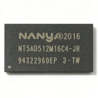
K4S510432D-UC75 - 512Mb SDRAM 133MHz 54-TSOP II | Samsung
MPN: K4S510432D-UC75 ✓ AktifK4S510432D-UC75 Ringkasan
Synchronous DRAM is a class of DRAM that interfaces with a system clock, allowing burst-mode data transfer synchronized to the memory controller rather than asynchronous row/column strobing. Within the memory hierarchy, SDRAM sits between legacy asynchronous DRAM and modern DDR generations, and remains the standard main-memory technology for legacy embedded systems, industrial controllers, and older PC platforms (PC133 era).
Key features of the K4S510432D include the D-die process node, fully synchronous operation to the positive clock edge, and a burst length of 1, 2, 4, 8, or full-page with sequential and interleave burst modes. CAS latency options of 2 or 3 allow the memory controller to trade access latency against clock speed. Auto-refresh and self-refresh modes are supported, along with power-down mode for reduced standby consumption.
Technically, the device uses CMOS circuitry with a four-bank architecture addressed via two bank-select pins, providing high effective bandwidth at 133 MHz. The LVTTL input/output structure simplifies interfacing with 3.3V memory controllers, FPGAs, and ASICs. The UC75 speed grade guarantees 133 MHz operation at CL3 and 100 MHz at CL2 across the commercial temperature range.
Typical applications include legacy industrial main memory, telecom line cards, set-top boxes, test and measurement instrumentation, and FPGA-based designs requiring 3.3V synchronous memory such as systems built around Lattice and Microsemi (now Microchip) FPGA families.
When designing with this SDRAM, ensure proper termination on the high-speed address/control bus and strictly observe refresh intervals (64 ms per 4096 rows typical for the class); omitting the mode-register-set sequence after power-up is the most common bring-up failure.
This page synthesizes distributor pricing, drop-in family alternatives, and practical design notes not consolidated in the manufacturer datasheet.
Alternatif penggantian untuk K4S510432D-UC75 — paket yang sama, pin-pada-pin kompatibel. Bagian paket yang berbeda memerlukan kerja ulang PCB diabaikan.
Variasi di dalam seri ini
Model-series yang sama yang kompatibel dengan penggantian K4S510432D-UC75 (sama faktor bentuk dan footprint) — berbeda di dalam CAS Latency, Memory Type, Package, RoHS Status, Technology.
K4S510432D-UC750
✅ Drop-In📋 Alternatif referensi (tidak dalam katalog)
K4S510432D-UC60
✅ Drop-In ⚠️ Spesifikasi Tidak Disahkan📋 Alternatif referensi (tidak dalam katalog)
K4S510432D-UC75T00
✅ Drop-In ⚠️ Spesifikasi Tidak DisahkanKontak untuk harga
Lihat Datasheet →K4S510432D-UC75T00
✅ Drop-InKontak untuk harga
Lihat Datasheet →K4S510432D-UC75 Spesifikasi
| Tipe Memori | SDRAM (Synchronous DRAM) |
| Ukuran Memori | 512 Mbit |
| Organisasi | 128M x 4 |
| Clock Frequency | 133 MHz |
| Access Time | 65 ns |
| Tipe Antarmuka | LVTTL |
| Supply Voltage Min | 3.0 V |
| Supply Voltage Max | 3.6 V |
| Technology | CMOS, D-die |
| Latensi CAS | 2 or 3 |
| Burst Length | 1, 2, 4, 8, full page |
| Refresh | Auto-refresh and self-refresh |
| Paket | 54-TSOP II (PDSO54, 0.80 mm pitch) |
| Package Dimensions | 0.400 x 0.875 inch (10.2 x 22.2 mm) |
| Tipe Mounting | Surface Mount |
| Suhu Kerja | Commercial temperature range |
| Status RoHS | RoHS compliant |
| Number of Terminals | 54 |
Konfigurasi Pin K4S510432D-UC75
| Pin produk 1 | VDD — Core power supply (3.0V to 3.6V) |
| Pin produk 2 | DQ0 — Data input/output bit 0 |
| Pin produk 3 | VDDQ — I/O power supply |
| Pin produk 4 | DQ1 — Data input/output bit 1 |
| Pin produk 5 | NC — Not connected (per datasheet) |
| Pin produk 6 | VDDQ — I/O power supply |
| Pin produk 7 | NC — Not connected (per datasheet) |
| Pin produk 8 | VDDQ — I/O power supply |
| Pin produk 9 | NC — Not connected (per datasheet) |
| Pin produk 10 | VDDQ — I/O power supply |
| Pin produk 11 | NC — Not connected (per datasheet) |
| Pin produk 12 | VSSQ — I/O ground |
| Pin produk 13 | NC — Not connected (per datasheet) |
| Pin produk 14 | VSSQ — I/O ground |
| Pin produk 15 | NC — Not connected (per datasheet) |
| Pin produk 16 | VSSQ — I/O ground |
| Pin produk 17 | NC — Not connected (per datasheet) |
| Pin produk 18 | VSSQ — I/O ground |
| Pin produk 19 | NC — Not connected (per datasheet) |
| Pin produk 20 | VSS — Core ground |
| Pin produk 21 | DQ2 — Data input/output bit 2 |
| Pin produk 22 | DQM — Data input/output mask |
| Pin produk 23 | WE — Write enable |
| Pin produk 24 | CAS — Column address strobe |
| Pin produk 25 | RAS — Row address strobe |
| Pin produk 26 | CS — Chip select |
| Pin produk 27 | BA0 — Bank address select 0 |
| Pin produk 28 | BA1 — Bank address select 1 |
| Pin produk 29 | A12 — Address input (row/column) |
| Pin produk 30 | A11 — Address input |
| Pin produk 31 | A9 — Address input |
| Pin produk 32 | A8 — Address input |
| Pin produk 33 | A7 — Address input |
| Pin produk 34 | A6 — Address input |
| Pin produk 35 | A5 — Address input |
| Pin produk 36 | A4 — Address input |
| Pin produk 37 | A3 — Address input |
| Pin produk 38 | A2 — Address input |
| Pin produk 39 | A1 — Address input |
| Pin produk 40 | A0 — Address input |
| Pin produk 41 | VDD — Core power supply |
| Pin produk 42 | VSS — Core ground |
| Pin produk 43 | CKE — Clock enable |
| Pin produk 44 | CLK — System clock input |
| Pin produk 45 | NC — Not connected (per datasheet) |
| Pin produk 46 | NC — Not connected (per datasheet) |
| Pin produk 47 | DQ3 — Data input/output bit 3 |
| Pin produk 48 | VSSQ — I/O ground |
| Pin produk 49 | NC — Not connected (per datasheet) |
| Pin produk 50 | VDDQ — I/O power supply |
| Pin produk 51 | NC — Not connected (per datasheet) |
| Pin produk 52 | VSSQ — I/O ground |
| Pin produk 53 | VDDQ — I/O power supply |
| Pin produk 54 | VSS — Core ground |
Aplikasi Umum
K4S510432D-UC75 cocok untuk 6 aplikasis: Legacy Industrial Main Memory, FPGA-Based Processing Systems, Telecom and Networking Line Cards, Set-Top Box and Consumer Multimedia, Test and Measurement Instrumentation, Aerospace and Defense Legacy Sustainment.
Legacy Industrial Main Memory
Industrial controllers, PLCs, and motion-control systems built in the PC133 era rely on 3.3V LVTTL SDRAM as main working memory. The K4S510432D-UC75 fits these designs directly: its 512Mbit capacity in 128M x 4 organization matches the 32-bit-wide buses formed by four x4 devices, and its 133 MHz rating with 65 ns access time comfortably supports the 100-133 MHz memory clocks common on PowerPC and ARM-class industrial SoCs. Because it is fully synchronous with CAS latency 2/3 programmability, existing SDRAM controllers need no firmware changes. RoHS compliance allows continued use in EU-market industrial equipment, and the commercial temperature range covers standard factory floor environments.
Direkomendasikan
FPGA-Based Processing Systems
The K4S510432D-UC75 serves as external working memory in FPGA systems, particularly with 3.3V LVTTL I/O families such as Microsemi ProASIC3 (A3P600) and RTAX radiation-tolerant devices whose banks natively drive 3.3V memory signaling. Its 133 MHz clock rate aligns with standard SDRAM controller IP offering CL2/CL3 latency, burst lengths of 1/2/4/8, and full-page modes for video or packet buffering. Because the x4 organization allows width expansion to x32/x64 with minimal fanout per data line, signal integrity at 133 MHz remains manageable on two-layer to four-layer boards. Designers must implement the mandatory initialization sequence: 100 us delay, precharge-all, eight auto-refresh cycles, then mode register set.
Direkomendasikan
Telecom and Networking Line Cards
Telecom line cards, E1/T1 framers, and legacy network processing platforms historically used banks of x4 SDRAM for deep packet buffering and statistics counters, where the narrow x4 organization enabled very wide ECC-protected buses. The K4S510432D-UC75 provides 512Mbit per device with LVTTL compatibility to the 3.3V backplane domain, 133 MHz operation for sustained buffering throughput, and full-page burst mode suited to sequential FIFO-like traffic. Four devices in x32 configuration deliver 2Gbit of buffered storage with auto-refresh handled transparently by the controller. Self-refresh mode permits line-card standby states without data loss, valuable in redundant carrier-grade architectures requiring hot-standby memory retention.
Direkomendasikan
Set-Top Box and Consumer Multimedia
Digital set-top boxes and consumer multimedia decoders of the early-2000s generation used 3.3V SDRAM for MPEG-2 video frame buffering. The K4S510432D-UC75 suits this role with 512Mbit density per device, 133 MHz clock for the ~800 MB/s aggregate bandwidth of a 64-bit bus, and CAS latency 3 timing at the video-refresh clock rates. Its LVTTL interface connects directly to the 3.3V memory controller in SoCs of that era, and its commercial temperature rating covers typical consumer operating environments. Full-page burst mode maximizes efficiency in the predominantly sequential access pattern of video frame buffers, and auto-refresh maintains picture data during decoder idle periods.
Direkomendasikan
Test and Measurement Instrumentation
Oscilloscope, logic analyzer, and data-acquisition platforms require deep sample memory; legacy instruments based on 3.3V SDRAM controllers use parts like the K4S510432D-UC75 for acquisition buffers. The 65 ns access time and CL2/CL3 programmability let designers tune latency versus throughput for streaming capture, while 1/2/4/8/full-page burst modes support both scattered-channel reads and high-speed sequential streaming. Four devices in x32 plus ECC-wide configurations give the error coverage needed for measurement credibility. The D-die CMOS process keeps standby power low for battery-powered portable instruments, and self-refresh preserves buffered waveforms through processor sleep states between analysis passes.
Direkomendasikan
Aerospace and Defense Legacy Sustainment
Aerospace and defense programs with 15-25 year lifecycles face recurring shortages of PC133-era SDRAM for avionics buffers, radar pre-processing memory, and ground-support equipment. The K4S510432D-UC75 sustains these designs with a pin-compatible Samsung family (UC60/UC75/UC750 grades) enabling supply-chain hedging through multiple qualified speed grades on the same footprint. Its fully static-friendly synchronous interface requires no redesign when substituting within the family, and RoHS compliance simplifies logistics for refurbished hardware. Radiation-tolerant system builders frequently pair commercial SDRAM with watchdog refresh schemes; the part's defined auto-refresh timing (4096 cycles per 64 ms) supports deterministic refresh scheduling in fault-tolerant memory managers.
Direkomendasikan
Ringkasan Produk Direkomendasikan
Data referensi engineering untuk K4S510432D-UC75 — pembandingan, panduan desain, dan informasi konformitas.
Panduan Pemilihan
Pembandingan dengan Alternatif
| Parameter Umum | Produk Ini | K4S510432D-UC750 | K4S510432D-UC60 | K4S510432D-UC7 | K4S510432D-UC75T00 |
|---|---|---|---|---|---|
| Package | 54-TSOP II | 54-TSOP II - same | 54-TSOP II - same | 54-TSOP II - same | 54-TSOP II - same |
| Brand | Samsung Electronics | Samsung Electronics | Samsung Electronics | Samsung Electronics | Samsung Electronics |
| Memory Size | 512 Mbit | 512 Mbit | 512 Mbit | 512 Mbit | 512 Mbit |
| Organization | 128M x 4 | 128M x 4 | 128M x 4 | 128M x 4 | 128M x 4 |
| Clock Frequency | 133 MHz | 133 MHz class | 100 MHz class | 133 MHz class | 133 MHz |
| Supply Voltage | 3.0 V to 3.6 V | 3.0 V to 3.6 V | 3.0 V to 3.6 V | 3.0 V to 3.6 V | 3.0 V to 3.6 V |
| Interface | LVTTL | LVTTL | LVTTL | LVTTL | LVTTL |
Diferensiator Kunci
- Highest speed grade within the K4S510432D family (vsK4S510432D-UC60)
- Tape-and-reel availability for volume production (vsK4S510432D-UC75T00)
- RoHS compliant D-die process (vsK4S510432D-UC750)
Catatan Desain
For 133 MHz SDRAM bus routing, keep CLK trace short and route all address/control signals as a matched group with controlled skew relative to clock (target < 500 ps skew for the D-die setup/hold budget). Use a solid ground plane under the memory bus, series-terminate address/control lines (22-33 ohm) and parallel-terminate data lines per controller driver strength. Decouple each VDD/VDDQ pin pair with 0.1 uF ceramic plus bulk 10 uF per device. Samsung application notes for D-die SDRAM provide reference AC timing parameters for CL3 at 133 MHz.
Power the device from a clean 3.3V rail (3.0-3.6V absolute window). Estimated: at typical operating current levels for 512Mb SDRAM of this class, four devices on a 64-bit bus draw on the order of a few hundred milliamps active; budget rail capacity accordingly and sequence power so VDD and VDDQ ramp together. CKE should be held low during power ramp to keep outputs tri-stated and prevent bus contention with the memory controller during controller initialization.
The most common bring-up failure is omitting or mis-ordering the initialization sequence: the controller must wait 100 us after stable power, issue PRECHARGE ALL, perform 8 AUTO REFRESH cycles, then set the mode register (CAS latency, burst length, burst type, write burst mode) before any access. A second frequent error is missing the 15.6 us refresh deadline (4096 cycles per 64 ms), producing intermittent bit errors instead of hard failure. Verify the speed-grade suffix on delivered parts: a UC60 cannot be assumed to close timing at 133 MHz.
Informasi Konformitas
RoHS compliant per distributor datasheet record (ROHS COMPLIANT, TSOP2-54). REACH, lead-free plating, halogen-free, and conflict-minerals statuses were not specified in the retrieved data - consult Samsung official product compliance declarations.