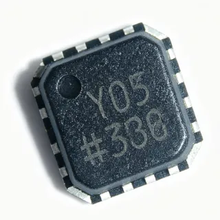
LMK00306SQX/NOPB - 3.1GHz 6-Output Clock Buffer | Texas Instruments
MPN: LMK00306SQX/NOPB ✓ AktifLMK00306SQX/NOPB Ringkasan
A clock buffer is a component that takes an input clock signal and generates multiple output copies with minimal added jitter and skew, ensuring signal integrity across multiple loads. It sits between a clock source (such as an oscillator or PLL) and downstream devices like ADCs, FPGAs, and SERDES, forming a critical part of the clock distribution network in high-speed digital systems. The LMK00306 belongs to the clock buffer family, which is a subset of clock and timing ICs within the broader semiconductor category.
Key features include ultra-low additive jitter of 50 fs RMS (typical) at 100 MHz, a wide input frequency range up to 3.1 GHz, and independent output bank power supplies (VCCO) for level translation. The device supports 3:7 fanout (3 inputs, 7 outputs) and offers pin-programmable output modes, making it highly configurable. Its low additive jitter ensures minimal degradation of the clock signal, critical for high-speed data converters and networking equipment.
Technically, the LMK00306 uses a differential input stage with internal termination resistors, and each output bank can be independently configured for LVPECL, LVDS, or HCSL signaling. The device includes an LVCMOS output for low-frequency monitoring or system clocking. The WQFN package with exposed pad provides excellent thermal performance, and the device operates from a 3.3V supply with separate VCCO pins for output level shifting.
Typical applications include clock distribution for high-speed ADCs/DACs, FPGA and ASIC clocking, networking switches and routers, and test and measurement equipment. Its low jitter and flexible level translation make it ideal for systems requiring precise timing across multiple boards.
When designing with this device, ensure proper termination of unused outputs and place decoupling capacitors close to each power pin. The exposed pad must be soldered to a thermal via array for optimal heat dissipation.
Alternatif penggantian untuk LMK00306SQX/NOPB — paket yang sama, pin-pada-pin kompatibel. Bagian paket yang berbeda memerlukan kerja ulang PCB diabaikan.
Variasi di dalam seri ini
Model-series yang sama yang kompatibel dengan penggantian LMK00306SQX/NOPB (sama faktor bentuk dan footprint) — berbeda di dalam Number of Outputs, Package.
LMK00306SQE/NOPB
✅ Drop-In📋 Alternatif referensi (tidak dalam katalog)
LMK00306SQ/NOPB
✅ Drop-In📋 Alternatif referensi (tidak dalam katalog)
LMK00804B
✅ Drop-In ⚠️ Spesifikasi Tidak Disahkan📋 Alternatif referensi (tidak dalam katalog)
NB7L1008M
✅ Drop-In ⚠️ Spesifikasi Tidak Disahkan📋 Alternatif referensi (tidak dalam katalog)
ADCLK946
✅ Drop-In ⚠️ Spesifikasi Tidak Disahkan📋 Alternatif referensi (tidak dalam katalog)
LMK00306SQX/NOPB Spesifikasi
| Fungsi | Clock Fanout Buffer (Distribution), Multiplexer, Translator |
| Input:Output Ratio | 3:7 |
| Maximum Input Frequency | 3.1 GHz |
| Additive Jitter | 50 fs RMS (typical) at 100 MHz |
| Jumlah Output | 6 differential + 1 LVCMOS |
| Output Logic Levels | LVPECL, LVDS, HCSL |
| Input Types | 2 universal inputs, 1 crystal input |
| Supply Voltage (VCC) | 3.3 V |
| Output Supply Voltage (VCCO) | 2.5 V to 3.3 V (per bank) |
| Rentang Suhu Kerja | -40°C to +85°C |
| Paket | 36-WFQFN Exposed Pad (NJK) |
| Tipe Mounting | Surface Mount |
| Status RoHS | Compliant |
| REACH Status | Compliant |
Konfigurasi Pin LMK00306SQX/NOPB
| Pin produk 1 | CLKIN0 — Differential input 0 (positive) |
| Pin produk 2 | CLKIN0* — Differential input 0 (negative) |
| Pin produk 3 | CLKIN1 — Differential input 1 (positive) |
| Pin produk 4 | CLKIN1* — Differential input 1 (negative) |
| Pin produk 5 | VCC — Main power supply (3.3V) |
| Pin produk 6 | GND — Ground |
| Pin produk 7 | CLKOUT0 — Differential output 0 (positive) |
| Pin produk 8 | CLKOUT0* — Differential output 0 (negative) |
| Pin produk 9 | VCCO0 — Output supply for bank 0 |
| Pin produk 10 | CLKOUT1 — Differential output 1 (positive) |
| Pin produk 11 | CLKOUT1* — Differential output 1 (negative) |
| Pin produk 12 | CLKOUT2 — Differential output 2 (positive) |
| Pin produk 13 | CLKOUT2* — Differential output 2 (negative) |
| Pin produk 14 | VCCO0 — Output supply for bank 0 (shared) |
| Pin produk 15 | CLKOUT3 — Differential output 3 (positive) |
| Pin produk 16 | CLKOUT3* — Differential output 3 (negative) |
| Pin produk 17 | CLKOUT4 — Differential output 4 (positive) |
| Pin produk 18 | CLKOUT4* — Differential output 4 (negative) |
| Pin produk 19 | VCCO1 — Output supply for bank 1 |
| Pin produk 20 | CLKOUT5 — Differential output 5 (positive) |
| Pin produk 21 | CLKOUT5* — Differential output 5 (negative) |
| Pin produk 22 | CLKOUT6 — LVCMOS output |
| Pin produk 23 | GND — Ground |
| Pin produk 24 | SEL0 — Input select 0 |
| Pin produk 25 | SEL1 — Input select 1 |
| Pin produk 26 | EN — Enable (active high) |
| Pin produk 27 | VCC — Main power supply (3.3V) |
| Pin produk 28 | GND — Ground |
| Pin produk 29 | CLKIN_XTAL — Crystal input |
| Pin produk 30 | CLKIN_XTAL* — Crystal input (complementary) |
| Pin produk 31 | GND — Ground |
| Pin produk 32 | VCC — Main power supply (3.3V) |
| Pin produk 33 | NC — No connect |
| Pin produk 34 | NC — No connect |
| Pin produk 35 | NC — No connect |
| Pin produk 36 | NC — No connect |
| Pin produk PAD | Exposed Pad — Thermal pad, connect to GND |
Aplikasi Umum
LMK00306SQX/NOPB cocok untuk 6 aplikasis: High-Speed ADC/DAC Clock Distribution, FPGA and ASIC Clocking, Networking and Communications, Test and Measurement Equipment, Broadcast Video and Audio, Aerospace and Defense.
High-Speed ADC/DAC Clock Distribution
The LMK00306SQX/NOPB provides ultra-low jitter clock distribution for high-speed data converters. Its 50 fs RMS additive jitter ensures that the sampling clock integrity is preserved, which is critical for achieving high SNR and SFDR in ADCs and DACs. The device can fan out a single clock to multiple converters, reducing skew and maintaining synchronization. With support for LVPECL, LVDS, and HCSL outputs, it can interface with various converter clock inputs. The 3.1-GHz maximum frequency accommodates the latest high-speed converters, while the configurable output banks allow independent voltage levels for different converter families.
Direkomendasikan
FPGA and ASIC Clocking
In FPGA and ASIC designs, the LMK00306SQX/NOPB distributes a clean clock to multiple logic blocks, ensuring timing closure and reducing clock skew. Its low additive jitter is essential for high-speed serial interfaces like PCIe, Ethernet, and JESD204B. The device's 3:7 fanout allows a single clock source to drive multiple FPGA banks or ASIC domains. The LVCMOS output can be used for system monitoring or as a low-frequency reference. The independent VCCO pins enable level translation between different I/O standards, simplifying board design. The WQFN package's small footprint is ideal for dense PCB layouts.
Direkomendasikan
Networking and Communications
The LMK00306SQX/NOPB is used in networking switches, routers, and line cards to distribute reference clocks to SERDES, PHYs, and switch fabrics. Its 3.1-GHz bandwidth supports high-speed Ethernet (100GbE) and optical transport. The low jitter ensures bit-error-rate (BER) performance meets industry standards. The device can translate between different logic levels, allowing it to interface with various PHY devices. The configurable outputs enable flexible clock tree design, reducing component count. The industrial temperature range makes it suitable for outdoor and harsh environment networking equipment.
Direkomendasikan
Test and Measurement Equipment
In test and measurement instruments, the LMK00306SQX/NOPB provides precise clock distribution for signal generators, oscilloscopes, and spectrum analyzers. Its ultra-low jitter is critical for maintaining measurement accuracy and repeatability. The device can fan out a reference clock to multiple measurement channels, ensuring synchronization. The level translation capability allows interfacing with different logic families used in test equipment. The wide frequency range supports various test signals. The compact WQFN package is suitable for benchtop and portable instruments.
Direkomendasikan
Broadcast Video and Audio
The LMK00306SQX/NOPB is used in broadcast video routers and audio mixing consoles to distribute word clocks and video sync signals. Its low jitter ensures stable audio/video synchronization, preventing artifacts. The device can translate between different clock standards, such as AES/EBU and SDI. The multiple outputs allow driving multiple devices from a single clock source. The LVCMOS output can be used for system control. The industrial temperature range is suitable for broadcast environments.
Direkomendasikan
Aerospace and Defense
In aerospace and defense systems, the LMK00306SQX/NOPB provides reliable clock distribution for radar, avionics, and communication systems. Its wide temperature range and low jitter ensure performance in harsh environments. The device can distribute clocks to multiple processing units, ensuring synchronization in mission-critical applications. The level translation capability allows interfacing with various military-grade logic. The compact package is suitable for space-constrained avionics. The device's high reliability makes it suitable for long-life defense programs.
Direkomendasikan
Ringkasan Produk Direkomendasikan
Data referensi engineering untuk LMK00306SQX/NOPB — pembandingan, panduan desain, dan informasi konformitas.
Panduan Pemilihan
Pembandingan dengan Alternatif
| Parameter Umum | Produk Ini | LMK00306SQE/NOPB | LMK00306SQ/NOPB | LMK00804B | NB7L1008M | ADCLK946 |
|---|---|---|---|---|---|---|
| Package | 36-WFQFN Exposed Pad (NJK) | 36-WFQFN Exposed Pad (NJK) | 36-WFQFN Exposed Pad (NJK) | 36-WFQFN Exposed Pad (NJK) | 36-WFQFN Exposed Pad (NJK) | 36-WFQFN Exposed Pad (NJK) |
| Brand | Texas Instruments | Texas Instruments | Texas Instruments | Texas Instruments | onsemi | Analog Devices |
| Maximum Input Frequency | 3.1 GHz | 3.1 GHz | 3.1 GHz | 2.5 GHz | 3.1 GHz | 2.4 GHz |
| Number of Outputs | 6 differential + 1 LVCMOS | 6 differential + 1 LVCMOS | 6 differential + 1 LVCMOS | 4 differential | 8 differential | 6 differential |
| Additive Jitter | 50 fs RMS (typ) | 50 fs RMS (typ) | 50 fs RMS (typ) | 100 fs RMS (typ) | 80 fs RMS (typ) | 60 fs RMS (typ) |
| Output Logic Levels | LVPECL, LVDS, HCSL | LVPECL, LVDS, HCSL | LVPECL, LVDS, HCSL | LVPECL, LVDS, HCSL | LVPECL, LVDS, HCSL | LVPECL, LVDS, HCSL |
| Supply Voltage | 3.3 V | 3.3 V | 3.3 V | 3.3 V | 3.3 V | 3.3 V |
| Operating Temperature Range | -40°C to +85°C | -40°C to +85°C | -40°C to +85°C | -40°C to +85°C | -40°C to +85°C | -40°C to +85°C |
Diferensiator Kunci
- Ultra-low additive jitter of 50 fs RMS (vsLMK00804B)
- Higher maximum frequency of 3.1 GHz (vsADCLK946)
- Same-brand drop-in compatibility (vsNB7L1008M)
Catatan Desain
Place decoupling capacitors (0.1uF and 10uF) close to each VCC and VCCO pin. The exposed pad must be soldered to a thermal via array connected to the ground plane to ensure proper heat dissipation and electrical grounding. Use a solid ground plane under the device to minimize noise.
For differential outputs, route as 100-ohm differential pairs with controlled impedance. Keep trace lengths matched to minimize skew. Terminate unused outputs with appropriate resistors (e.g., 100-ohm across differential pairs) to prevent reflections and reduce EMI.
Ensure the input clock source is clean and within the specified frequency range. Avoid routing clock traces near high-speed switching signals. Use the SEL pins to select the correct input and configure output banks properly. Do not leave enable pin floating; tie it to VCC for always-on operation.
Informasi Konformitas
RoHS and REACH compliant per Abacus Technologies. Not AEC-Q100 qualified.