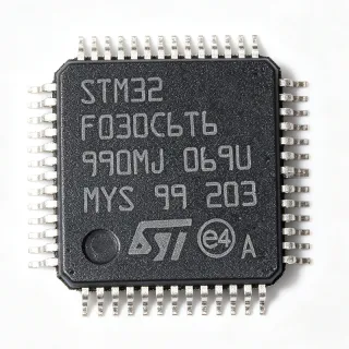
MC9S12C32MFAE16 - HCS12 16-Bit MCU 32KB Flash LQFP-48 | NXP
MPN: MC9S12C32MFAE16 ✗ Akhir HidupMC9S12C32MFAE16 Ringkasan
A microcontroller (MCU) is a single-chip computer containing a CPU core, program and data memory, and integrated peripherals such as timers, communication interfaces (SCI/SPI/I2C), and analog-to-digital converters. The HCS12C belongs to the broader HCS12 family of 16-bit CISC microcontrollers, optimized for deterministic real-time control in body electronics, sensor interfacing, and LIN-connected automotive nodes. Within the embedded hierarchy, MCUs sit below microprocessors (MPUs) and above standard logic ICs, providing an autonomous compute engine with on-chip non-volatile storage for firmware.
Key differentiating features of the MC9S12C32MFAE16 include 32KB Flash, 2KB RAM, 1KB EEPROM, an 8-channel 10-bit ADC, up to 38 general-purpose I/O lines, an enhanced capture/timer module, and background debug mode (BDM) for in-circuit programming and debug. The integrated on-chip bandgap voltage regulator and phase-locked loop simplify power and clock tree design, removing the need for external regulators or oscillator tuning networks.
Architecturally, the HCS12 core uses a 16-bit data path with a memory-management unit that unifies Flash, RAM, and EEPROM into a linear 64KB address space, supporting C and assembly firmware development through NXP's CodeWarrior and the GCC-based Eclipse toolchains. The peripheral module library is fully documented in NXP reference manuals, allowing deterministic interrupt-driven design with 16-bit timer prescalers and pulse-width modulation for motor and lighting loads.
Typical applications include automotive body controllers, HVAC actuators, instrument clusters, and LIN/CAN-connected sensor nodes, as well as industrial general-purpose control where its 16-bit performance and 32KB flash capacity meet firmware size budgets. The 48-pin LQFP footprint makes it suitable for through-hole-compatible hand-rework prototypes and high-volume surface-mount assembly.
Designers should allocate the VDD/VSS pins per the package pinout to ensure stable supply for the on-chip voltage regulator, place decoupling capacitors close to all VDD pins, and route the oscillator traces symmetrically when using an external crystal. The BDM interface requires a dedicated debug header for in-circuit programming; this must be considered in the PCB layout to avoid post-layout rework.
This page synthesizes distributor stock, lifecycle status, drop-in alternatives, and design notes not found on a single manufacturer or distributor page, enabling engineers to evaluate the MC9S12C32MFAE16 for new designs and legacy migration.
Alternatif penggantian untuk MC9S12C32MFAE16 — paket yang sama, pin-pada-pin kompatibel. Bagian paket yang berbeda memerlukan kerja ulang PCB diabaikan.
Variasi di dalam seri ini
Model-series yang sama yang kompatibel dengan penggantian MC9S12C32MFAE16 (sama faktor bentuk dan footprint) — berbeda di dalam On-chip Voltage Regulator, Package, Program Memory Size, RAM Size, Supply Voltage.
MC9S12C32CFAE16
✅ Drop-In📋 Alternatif referensi (tidak dalam katalog)
MC9S12C32CFUE16
✅ Drop-In📋 Alternatif referensi (tidak dalam katalog)
MC9S12C32VFAE16
✅ Drop-InKontak untuk harga
Lihat Datasheet →MC9S12C64MFAE16
✅ Drop-In📋 Alternatif referensi (tidak dalam katalog)
MC9S12GC32MFAE
✅ Drop-InKontak untuk harga
Lihat Datasheet →MC9S12GC16MFAE
✅ Drop-InKontak untuk harga
Lihat Datasheet →MC9S12C32MFAE16 Rating Maksimal & Karakteristik Listrik
| Core Architecture | HCS12 (16-bit CISC) |
| Family | S12C |
| Program Memory | 32 KB Flash |
| RAM | 2 KB |
| EEPROM | 1 KB |
| Bus Clock / CPU Frequency | 16 MHz |
| Supply Voltage (VDD) | 2.97 V to 5.5 V (5 V nominal, 2.5 V mode supported) |
| Paket | 48-pin LQFP (7x7 mm) |
| Tipe Mounting | Surface Mount |
| GPIO Count | Up to 38 |
| ADC | 8-channel, 10-bit |
| Communication Interfaces | SCI (UART), SPI, I2C |
| Timers | Enhanced Capture Timer (ECT) + PWM channels |
| On-chip Voltage Regulator | Yes (bandgap-based VREG) |
| On-chip PLL | Yes |
| Debug Interface | Background Debug Mode (BDM) |
| Suhu Kerja | -40 C to +85 C (automotive grade) |
Konfigurasi Pin MC9S12C32MFAE16
| Pin produk 1 | XCLKS — External clock selection |
| Pin produk 2 | VDDR — External power for regulator |
| Pin produk 3 | VDD — Digital supply voltage |
| Pin produk 4 | VSS — Digital ground |
| Pin produk 5 | RESET — Active-low reset input |
| Pin produk 6 | MODC — Mode selection |
| Pin produk 7 | BKGD — Background Debug Mode pin |
| Pin produk 8 | PE7 — GPIO / ECT |
| Pin produk 9 | PE6 — GPIO / ECT |
| Pin produk 10 | PE5 — GPIO / ECT |
| Pin produk 11 | PE4 — GPIO / ECT |
| Pin produk 12 | VSS — Digital ground |
| Pin produk 13 | VDD — Digital supply voltage |
| Pin produk 14 | PA7 — GPIO / SCI TX |
| Pin produk 15 | PA6 — GPIO / SCI RX |
| Pin produk 16 | PA5 — GPIO / timer |
| Pin produk 17 | PA4 — GPIO / timer |
| Pin produk 18 | PA3 — GPIO / timer |
| Pin produk 19 | PA2 — GPIO / timer |
| Pin produk 20 | PA1 — GPIO / ADC |
| Pin produk 21 | PA0 — GPIO / ADC |
| Pin produk 22 | VDDA — Analog supply voltage |
| Pin produk 23 | VSSA — Analog ground |
| Pin produk 24 | PB7 — GPIO / SPI / I2C |
| Pin produk 25 | PB6 — GPIO / SPI / I2C |
| Pin produk 26 | PB5 — GPIO / SPI / I2C |
| Pin produk 27 | PB4 — GPIO / SPI / I2C |
| Pin produk 28 | PB3 — GPIO / SPI / I2C |
| Pin produk 29 | PB2 — GPIO / SPI / I2C |
| Pin produk 30 | PB1 — GPIO / SPI / I2C |
| Pin produk 31 | PB0 — GPIO / SPI / I2C |
| Pin produk 32 | VSS — Digital ground |
| Pin produk 33 | VDD — Digital supply voltage |
| Pin produk 34 | PC7 — GPIO / GPIO-only |
| Pin produk 35 | PC6 — GPIO / GPIO-only |
| Pin produk 36 | PC5 — GPIO / GPIO-only |
| Pin produk 37 | PC4 — GPIO / GPIO-only |
| Pin produk 38 | PC3 — GPIO / GPIO-only |
| Pin produk 39 | PC2 — GPIO / GPIO-only |
| Pin produk 40 | PC1 — GPIO / GPIO-only |
| Pin produk 41 | PC0 — GPIO / GPIO-only |
| Pin produk 42 | VSS — Digital ground |
| Pin produk 43 | VDD — Digital supply voltage |
| Pin produk 44 | PD7 — GPIO / PWM |
| Pin produk 45 | PD6 — GPIO / PWM |
| Pin produk 46 | PD5 — GPIO / PWM |
| Pin produk 47 | PD4 — GPIO / PWM |
| Pin produk 48 | PD3 — GPIO / PWM / XIRQ |
Aplikasi Umum
MC9S12C32MFAE16 cocok untuk 6 aplikasis: Automotive Body Control Modules, HVAC Actuator and Fan Controllers, Industrial Sensor Interfaces and IO Link Modules, Instrument Cluster Sub-Controllers, Battery Management Slave Nodes, General-Purpose Industrial Control.
Automotive Body Control Modules
The MC9S12C32MFAE16's 16-bit HCS12 core at 16 MHz, 32 KB Flash, and integrated SCI/SPI peripherals make it a strong fit for automotive body controllers managing lighting, door modules, and accessory loads. The on-chip bandgap regulator (VREG) accepts 2.97-5.5 V inputs, supporting direct connection to 12 V automotive rails via a simple external regulator chain. Its automotive-grade temperature range of -40 to +85 C ensures reliable operation in cabin and under-hood environments. Compared to 8-bit MCUs, the 16-bit HCS12 architecture reduces firmware complexity for door-mirror control and window-lift sequencing, while the Background Debug Mode (BDM) interface simplifies in-circuit flash programming during vehicle production.
Direkomendasikan
HVAC Actuator and Fan Controllers
For HVAC damper and blower controllers, the MC9S12C32MFAE16 provides an Enhanced Capture Timer with PWM channels ideally suited to drive brushless DC fans, stepper-motor damper actuators, and resistive heaters. Its 8-channel 10-bit ADC reads temperature sensors, pressure transducers, and potentiometer setpoints, while the on-chip PLL locks the bus clock to a precision reference for stable PWM frequency generation. The 32 KB Flash comfortably holds control loops and state-machine firmware for cabin climate regulation. Compared to discrete analog controllers, the integrated MCU reduces PCB area and enables diagnostic features like fault logging and over-temperature shutdown via the on-chip timers.
Direkomendasikan
Industrial Sensor Interfaces and IO Link Modules
The MC9S12C32MFAE16's SCI (UART), SPI, and I2C interfaces make it an ideal gateway MCU for industrial sensor hubs that aggregate data from multiple sensor types into a higher-level fieldbus (PROFIBUS, Modbus, or proprietary serial protocols). With 32 KB Flash, designers can implement both the sensor-acquisition state machine and the fieldbus protocol stack in firmware without off-chip memory. The integrated bandgap voltage regulator provides stable logic rails across the 5 V industrial supply range, simplifying the analog front-end design. Compared to 8-bit MCU alternatives, the 16-bit HCS12 architecture handles larger Modbus tables and CRC calculations in less CPU time, reducing per-frame response latency.
Direkomendasikan
Instrument Cluster Sub-Controllers
Within a digital instrument cluster, the MC9S12C32MFAE16 can serve as a sub-controller that reads analog gauge sensors via its 8-channel 10-bit ADC and broadcasts processed values over SPI to the main graphics MCU. Its up to 38 GPIO lines directly drive LED backlights and indicator lamps without external shift registers, while the 32 KB Flash holds lookup tables for fuel/coolant/temperature curves. The automotive-grade qualification is essential for the under-dash environment, with sustained operation across -40 C cold-start and +85 C hot-soak conditions. The BDM interface allows post-assembly firmware updates of warning thresholds without dismantling the cluster.
Direkomendasikan
Battery Management Slave Nodes
The MC9S12C32MFAE16's combination of 10-bit ADC, SCI, and timer modules suits it for Li-ion battery-management slave modules that monitor individual cell voltages and temperatures in a stacked battery pack. Each slave node converts cell voltages via the on-chip ADC and forwards measurements through an isolated SCI daisy chain to the master BMS controller. The 32 KB Flash accommodates look-up tables for cell-balancing thresholds and SOC estimation routines. Operating from a 5 V rail derived from the cell stack with the on-chip VREG, the MC9S12C32MFAE16 streamlines the analog front-end and reduces PCB area in compact battery modules. The integrated 16-bit PWM timers drive active-balancing MOSFET gates with precise duty cycle control.
Direkomendasikan
General-Purpose Industrial Control
Beyond automotive, the MC9S12C32MFAE16 is widely used in general-purpose industrial controllers where its mix of Flash size, peripheral count, and BDM-supported firmware development accelerates product development. Its extended -40 to +85 C temperature range and on-chip bandgap regulator simplify integration into factory-automation equipment operating from 5 V or 3.3 V supply rails. Common use cases include conveyor-belt motor controllers, valve actuators, simple PLCs, and dispenser pumps where 8-bit MCUs run out of code space and ARM Cortex-M0 devices are over-budget. The BDM-based in-circuit debug allows engineers to step through state machines and interrupts during commissioning, accelerating fault-finding in field installations.
Direkomendasikan
Ringkasan Produk Direkomendasikan
Data referensi engineering untuk MC9S12C32MFAE16 — pembandingan, panduan desain, dan informasi konformitas.
Panduan Pemilihan
Pembandingan dengan Alternatif
| Parameter Umum | Produk Ini | MC9S12C32CFAE16 | MC9S12C32CFUE16 | MC9S12C32VFAE16 | MC9S12C64MFAE16 | MC9S12GC32MFAE | MC9S12GC16MFAE |
|---|---|---|---|---|---|---|---|
| Brand | NXP Semiconductors | NXP Semiconductors | NXP Semiconductors | NXP Semiconductors | NXP Semiconductors | NXP Semiconductors | NXP Semiconductors |
| Package | 48-LQFP (7x7) | 48-LQFP (7x7) - same | 48-LQFP (7x7) - same | 48-LQFP (7x7) - same | 48-LQFP (7x7) - same | 48-LQFP (7x7) - same | 48-LQFP (7x7) - same |
| Core / Family | HCS12 / S12C | HCS12 / S12C - same | HCS12 / S12C - same | HCS12 / S12C - same | HCS12 / S12C - same | HCS12 / S12GC (upgrade) | HCS12 / S12GC (upgrade) |
| Bus Clock | 16 MHz | 16 MHz | 16 MHz | 16 MHz | 16 MHz | 25 MHz (higher) | 25 MHz (higher) |
| Flash Size | 32 KB | 32 KB - same | 32 KB - same | 32 KB - same | 64 KB (+100%) | 32 KB - same | 16 KB (-50%) |
| RAM | 2 KB | 2 KB | 2 KB | 2 KB | 2 KB | 2-4 KB (variant dependent) | 1-2 KB (variant dependent) |
| Operating Temperature | -40 to +85 C (automotive grade) | 0 to +70 C (commercial) | 0 to +70 C (commercial) | -40 to +105 C (extended automotive) | -40 to +85 C (automotive) | -40 to +85 C (automotive) | -40 to +85 C (automotive) |
| Lifecycle | NRND | NRND | Active (commercial) | NRND | NRND | Active | Active |
| On-chip Voltage Regulator | Yes (bandgap VREG) | Yes (bandgap VREG) | Yes (bandgap VREG) | Yes (bandgap VREG) | Yes (bandgap VREG) | Yes (bandgap VREG) | Yes (bandgap VREG) |
Diferensiator Kunci
- Integrated on-chip VREG with 2.97-5.5 V supply range (vsMC9S12C32CFAE16)
- 32 KB Flash with S12C peripheral set (vsMC9S12GC16MFAE)
- Industry-standard HCS12 toolchain ecosystem (vsMC9S12C32VFAE16)
Catatan Desain
Place decoupling capacitors (100 nF ceramic + 4.7 uF bulk) as close as physically possible to every VDD/VSS pair on the 48-pin LQFP. Use a solid VSS pour under the exposed pad area even though this LQFP has no exposed thermal pad; the ground pour reduces digital switching noise coupling into the analog ADC inputs. Estimated: decoupling loop area should be kept below 5 mm^2 for switching transients below 50 mVpp.
Do not leave the MODC pin floating - its state at reset selects between normal single-chip mode and expanded modes; a 4.7 kohm pull-up to VDD or pull-down to VSS is mandatory. According to the NXP S12C reference manual, an unterminated MODC pin can lock the MCU in BDM-only mode, preventing firmware execution and requiring BDM intervention to recover.
The Background Debug Mode (BKGD) pin requires a 4.7 kohm pull-up to VDD during reset; leaving it floating can cause spurious resets or unpredictable boot behavior, especially in electrically noisy automotive environments. Design must reserve enough PCB real estate for the 6-pin BDM header (BKGD, RESET, GND, VDD, MODC, optional TRST), or include test-pad access for in-circuit programming. Schematic review should call out the BKGD pull-up explicitly to avoid rework during EMC qualification.
The 10-bit ADC samples at up to ~6 us per conversion with channel-to-channel crosstalk below 1 LSB on quiet inputs; however, digital outputs switching within 50 mm of analog input traces can inject noise. Per NXP layout guidelines, route analog inputs on the opposite PCB layer from switching digital lines, and surround analog traces with a ground guard ring tied to VSSA. Estimated: with proper guarding and 100 nF + 10 nF analog supply decoupling, ADC SNR remains within datasheet-specified limits at full-scale conversion rates.
Informasi Konformitas
Compliance markers flagged as unknown because the verified web data did not include part-specific RoHS/REACH/AEC-Q100 declarations. Verify with NXP's material compliance database by part marking for the exact shipped date code before quoting to automotive customers.