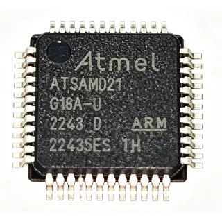
PIC24FJ128GL405-E/PT - 16-bit 32MHz 128KB Flash MCU w/ USB & LCD | Microchip
MPN: PIC24FJ128GL405-E/PT ✓ AktifPIC24FJ128GL405-E/PT Ringkasan
A 16-bit PIC24F microcontroller is a member of Microchip's high-performance, low-power MCU family, positioned in the broader taxonomy as: microcontroller -> embedded MCU -> 16-bit MCU -> PIC24F family -> PIC24FJ GL4 sub-family. PIC24F devices are widely used in human-machine interface (HMI), medical instrumentation, and battery-powered embedded systems because they balance MIPS throughput with deep-sleep current in the nanoamp range and integrate rich peripheral sets.
Key features include Dual Partition Flash supporting real-time Over-The-Air (OTA) firmware updates and EEPROM emulation, Core Independent Peripherals (CIPs) such as CLC, MCCP, and 32-bit CRC, a 10-bit/12-bit ADC with CTMU support, multiple UART/SPI/I2C interfaces, and a segmented LCD driver with charge pump. The device supports operating voltages from 2.0V to 3.6V and industrial-grade temperature range of -40C to +125C for the /E variant.
Technically, the PIC24FJ128GL405 employs a modified Harvard architecture with a 16-bit data path and 24-bit instruction word, allowing efficient C-compiled code. Hardware multiply/divide and a deterministic interrupt controller support real-time control loops. The integrated USB 2.0 full-speed transceiver eliminates an external PHY, saving BOM cost and PCB area for HID, CDC, or vendor-class peripherals.
Typical applications include low-power HMI with LCD readouts (thermostats, blood-pressure monitors), USB HID peripherals (keyboards, barcode scanners, game controllers), home medical devices with battery operation, e-metering with segmented LCD display, secure OTA-updatable IoT edge nodes, and industrial sensor transmitters requiring CIP-based deterministic behavior.
When designing with this device, allocate at least one of the two CRC/Scan hardware blocks to memory integrity verification if OTA updates are deployed. The segmented LCD driver requires bias-resistor network selection based on display duty cycle; consult the datasheet's LCD reference design.
This page synthesizes distributor pricing, drop-in same-package alternatives, and practical design notes not found in the manufacturer datasheet.
Alternatif penggantian untuk PIC24FJ128GL405-E/PT — paket yang sama, pin-pada-pin kompatibel. Bagian paket yang berbeda memerlukan kerja ulang PCB diabaikan.
Variasi di dalam seri ini
Model-series yang sama yang kompatibel dengan penggantian PIC24FJ128GL405-E/PT (sama faktor bentuk dan footprint) — berbeda di dalam Package, Operating Temperature, USB, Core Architecture, ADC.
PIC24FJ128GL406-I/PT
✅ Drop-In ⚠️ Spesifikasi Tidak DisahkanKontak untuk harga
Lihat Datasheet →PIC24FJ128GL305-I/PT
✅ Drop-In ⚠️ Spesifikasi Tidak Disahkan📋 Alternatif referensi (tidak dalam katalog)
PIC24FJ128GL306-I/PT
✅ Drop-In ⚠️ Spesifikasi Tidak Disahkan📋 Alternatif referensi (tidak dalam katalog)
PIC24FJ128GL403-I/PT
✅ Drop-In ⚠️ Spesifikasi Tidak Disahkan📋 Alternatif referensi (tidak dalam katalog)
PIC24FJ128GL306T-I/MR
✅ Drop-InKontak untuk harga
Lihat Datasheet →PIC24FJ128GC006T-I/PT
✅ Drop-InKontak untuk harga
Lihat Datasheet →PIC24FJ128GL405-E/PT Rating Maksimal & Karakteristik Listrik
| Core Architecture | PIC24F (16-bit modified Harvard) |
| Maximum CPU Speed | 32 MHz (16 MIPS) |
| Program Flash Memory | 128 KB |
| RAM | 32 KB |
| USB Interface | USB 2.0 Full-Speed Device, integrated transceiver |
| LCD Controller | Segmented LCD driver with charge pump |
| ADC | 10-bit / 12-bit with CTMU |
| Operating Voltage Range | 2.0 V to 3.6 V |
| Rentang Suhu Kerja | -40 C to +125 C (E variant) |
| Paket | 48-pin TQFP (7x7 mm) |
| Tipe Mounting | Surface Mount |
| Core Independent Peripherals (CIPs) | CLC, MCCP/SCCP, CRC, DMA, RTCC |
| Communication Interfaces | UART, SPI, I2C |
| Flash Partitioning | Dual Partition for OTA updates and EEPROM emulation |
| Status RoHS | Compliant |
Konfigurasi Pin PIC24FJ128GL405-E/PT
| Pin produk 1 | SDA3/RG3 — I2C3 data or general I/O |
| Pin produk 2 | SCL3/RG2 — I2C3 clock or general I/O |
| Pin produk 3 | RA0 — Analog input AN0 / general I/O |
| Pin produk 4 | RA1 — Analog input AN1 / general I/O |
| Pin produk 5 | RB0/PGED3 — Programming data / general I/O |
| Pin produk 6 | RB1/PGEC3 — Programming clock / general I/O |
| Pin produk 7 | RB2 — General I/O |
| Pin produk 8 | RB3 — General I/O |
| Pin produk 9 | VSS — Ground reference |
| Pin produk 10 | VDD — Positive supply (2.0-3.6V) |
| Pin produk 11 | RB4 — General I/O |
| Pin produk 12 | RB5 — General I/O |
| Pin produk 13 | RB6 — General I/O |
| Pin produk 14 | RB7 — General I/O |
| Pin produk 15 | RC0 — General I/O |
| Pin produk 16 | RC1 — General I/O |
| Pin produk 17 | RC2 — General I/O |
| Pin produk 18 | RC3 — General I/O |
| Pin produk 19 | VSS — Ground reference |
| Pin produk 20 | VDD — Positive supply (2.0-3.6V) |
| Pin produk 21 | RC4 — General I/O |
| Pin produk 22 | RC5 — General I/O |
| Pin produk 23 | RC6 — General I/O / UART TX |
| Pin produk 24 | RC7 — General I/O / UART RX |
| Pin produk 25 | RD0 — General I/O |
| Pin produk 26 | RD1 — General I/O |
| Pin produk 27 | RD2 — General I/O |
| Pin produk 28 | RD3 — General I/O |
| Pin produk 29 | RD4 — General I/O |
| Pin produk 30 | RD5 — General I/O |
| Pin produk 31 | RD6 — General I/O |
| Pin produk 32 | RD7 — General I/O |
| Pin produk 33 | RE0 — General I/O |
| Pin produk 34 | RE1 — General I/O |
| Pin produk 35 | RE2 — General I/O |
| Pin produk 36 | RE3 — General I/O |
| Pin produk 37 | RE4 — General I/O |
| Pin produk 38 | RE5 — General I/O |
| Pin produk 39 | RE6 — General I/O |
| Pin produk 40 | RE7 — General I/O |
| Pin produk 41 | RF0 — General I/O / LCD segment |
| Pin produk 42 | RF1 — General I/O / LCD segment |
| Pin produk 43 | RF2 — General I/O / LCD segment |
| Pin produk 44 | RF3 — General I/O / LCD segment |
| Pin produk 45 | RF4 — General I/O / USB D- |
| Pin produk 46 | RF5 — General I/O / USB D+ |
| Pin produk 47 | VBUS — USB VBUS sense input |
| Pin produk 48 | RF6/VCAP — Core regulator output, requires 10uF+0.1uF cap |
Aplikasi Umum
PIC24FJ128GL405-E/PT cocok untuk 6 aplikasis: Low-Power HMI with Segmented LCD, USB HID Peripherals (Keyboard, Barcode Scanner, Game Controller), Battery-Powered Medical Devices, Secure OTA-Updatable IoT Edge Nodes, Industrial Sensor Transmitters with CIPs, Electronic Metering with LCD Readout.
Low-Power HMI with Segmented LCD
The PIC24FJ128GL405-E/PT's integrated segmented LCD controller with charge pump drives glass displays directly from the 3.3V rail, eliminating an external -VEE inverter that would otherwise consume quiescent current. With 32 KB of RAM and 128 KB of Flash, the MCU can host button-debounce state machines, custom glyph tables, and Unicode font rendering for thermostats, blood-pressure monitors, and weighing scales. Its nanoamp-range deep-sleep current combined with RTCC wakeup allows coin-cell or 2xAA battery operation for 5+ years.
Direkomendasikan
USB HID Peripherals (Keyboard, Barcode Scanner, Game Controller)
The integrated USB 2.0 Full-Speed device transceiver with on-chip pull-up simplifies HID-class peripheral design and eliminates an external PHY, saving approximately 0.50 USD BOM cost. The 32 MHz / 16 MIPS core supports USB polling intervals down to 1 ms while still executing HID report parsing, debounce, and LED-status logic in firmware. Dual Partition Flash enables field firmware updates via USB without a programmer, which is critical for deployed HID peripherals that cannot be returned for service.
Direkomendasikan
Battery-Powered Medical Devices
The PIC24FJ128GL405-E/PT's eXtreme Low-Power architecture with deep-sleep current below 1 uA enables battery-powered medical devices such as portable pulse oximeters, glucose meters, and electronic thermometers to achieve multi-year coin-cell battery life. The 10-bit/12-bit ADC with CTMU supports accurate sensor readout for temperature, conductivity, and optical measurements. The extended -40C to +125C temperature range suits sterilization and refrigerated storage environments per common medical-device qualification requirements.
Direkomendasikan
Secure OTA-Updatable IoT Edge Nodes
Dual Partition Flash allows the PIC24FJ128GL405-E/PT to perform Over-The-Air firmware updates with zero downtime: while the application runs from Partition A, the new image is written to Partition B, then a bootloader swaps the active partition on next reset. Combined with the 32-bit hardware CRC, this provides tamper-detection and image-integrity verification required for IEC 62443-style edge-node security. USB can serve as the OTA transport (CDC class) during maintenance windows, removing the need for an external bootloader programmer.
Direkomendasikan
Industrial Sensor Transmitters with CIPs
Core Independent Peripherals (CIPs) like the Configurable Logic Cell (CLC), Multiple Capture/Compare/PWM (MCCP), and 32-bit CRC offload sensor-fusion, signal-conditioning, and data-integrity tasks from the CPU, allowing deterministic interrupt-free operation in industrial sensor transmitters. The integrated ADC with CTMU supports RTD, thermocouple, and 4-20 mA current-loop signal chains. Extended -40C to +125C temperature range and 3.6V absolute maximum tolerate harsh factory-floor environments with induced surge events.
Direkomendasikan
Electronic Metering with LCD Readout
Energy and water meters benefit from the PIC24FJ128GL405-E/PT's combination of segmented LCD controller (for kWh display), RTC with calendar (for time-of-use billing), and 10/12-bit ADC for current-sensing front ends. The deep-sleep current below 1 uA allows battery-backed metrology operation during mains outages. Hardware CRC and Dual Partition Flash support signed firmware-image verification, which is increasingly required by smart-meter security standards such as IEC 62056 and DLMS/COSEM.
Direkomendasikan
Ringkasan Produk Direkomendasikan
Data referensi engineering untuk PIC24FJ128GL405-E/PT — pembandingan, panduan desain, dan informasi konformitas.
Panduan Pemilihan
Pembandingan dengan Alternatif
| Parameter Umum | Produk Ini | PIC24FJ128GL406-I/PT | PIC24FJ128GL305-I/PT | PIC24FJ128GL306-I/PT | PIC24FJ128GC006T-I/PT |
|---|---|---|---|---|---|
| Brand | Microchip Technology | Microchip Technology | Microchip Technology | Microchip Technology | Microchip Technology |
| Package | TQFP-48 (7x7 mm) | TQFP-48 (7x7 mm) - same | TQFP-48 (7x7 mm) - same | TQFP-48 (7x7 mm) - same | TQFP-48 (7x7 mm) - same |
| Program Flash | 128 KB | 256 KB | 64 KB | 64 KB | 128 KB |
| RAM | 32 KB | 32 KB | 16 KB | 16 KB | 32 KB |
| USB | Full-Speed integrated | Full-Speed integrated | Full-Speed integrated | Full-Speed integrated | Full-Speed integrated |
| LCD Controller | Yes (segmented, charge pump) | Yes | Yes | Yes | Yes |
| Operating Voltage | 2.0 V to 3.6 V | 2.0 V to 3.6 V | 2.0 V to 3.6 V | 2.0 V to 3.6 V | 2.0 V to 3.6 V |
| Temperature Range | -40 C to +125 C (E) | -40 C to +85 C (I) | -40 C to +85 C (I) | -40 C to +85 C (I) | -40 C to +85 C (I) |
Diferensiator Kunci
- Extended -40C to +125C temperature range (E suffix) (vsPIC24FJ128GL406-I/PT)
- Optimal Flash/RAM balance (128 KB / 32 KB) (vsPIC24FJ128GL305-I/PT)
- Dual Partition Flash with hardware CRC for secure OTA (vsPIC24FJ128GB410-I/PT)
Catatan Desain
Estimated: at 32 MHz active, the PIC24FJ128GL405 draws approximately 15 mA from a 3.3V supply; deep-sleep current is below 1 uA per the datasheet. Place a 10 uF + 0.1 uF ceramic decoupling pair within 2 mm of each VDD/VSS pair on the TQFP-48 footprint. The VCAP pin (RF6/VCAP) requires a 10 uF + 0.1 uF capacitor to stabilize the internal 1.8V core regulator; omitting it causes POR failures and erratic reset behavior.
Keep the USB D+/D- traces (RF4, RF5) matched within 2 mm length and routed over a continuous ground plane to maintain 90 ohm differential impedance per USB 2.0 specification. Place the 15 kohm pull-down resistors on D+/D- close to the MCU. Avoid routing USB signals near switching regulators or RF traces to minimize common-mode noise that would corrupt USB eye-pattern compliance.
When using Dual Partition Flash for OTA updates, ensure the bootloader linker script reserves the upper Flash region as the inactive partition. A common pitfall is allocating the entire 128 KB to the application, leaving no room for the new-image staging partition. Also, configure the FSEC (Flash Security) bits after OTA validation - failing to lock the bootloader vector allows a malicious image to redirect execution.
The segmented LCD bias pins (SEG/COM) should be routed with a ground-shielded guard ring to prevent crosstalk into adjacent analog ADC inputs. Place the LCD bias-resistor network within 5 mm of the LCD connector to minimize trace resistance, which degrades display contrast at low temperature.
Informasi Konformitas
RoHS compliant per Microchip product page. PIC24FJ GL4 family is supported by Microchip's functional-safety documentation package for IEC 61508 SIL 2 capable designs but is not formally AEC-Q100 qualified - for automotive qualification use PIC24F KA/GB families with -E temperature grade.