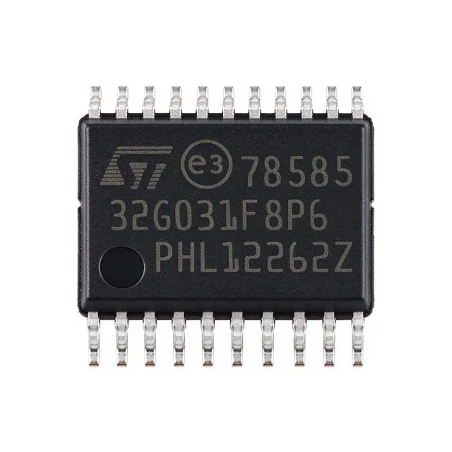
STM32G031F8P6 - 64MHz Cortex-M0+ MCU, 64KB Flash | STMicroelectronics
MPN: STM32G031F8P6 ✓ Aktif| Kwantitas | Harga Satuan | Lengkap |
|---|---|---|
| 1 | $1.8281 | $1,83 |
| 10 | $1.3203 | $13,20 |
| 100 | $1.168 | $116,80 |
| 500 | $1.1172 | $558,60 |
| 1.000 | $1.0664 | $1.066,40 |
STM32G031F8P6 Ringkasan
An MCU (microcontroller) is a single-chip computer that integrates a CPU core, program memory (Flash), data memory (SRAM), and programmable peripherals into one package. The Cortex-M0+ is Arm's smallest and most energy-efficient 32-bit core, sitting in the hierarchy: Cortex-M0+ -> Arm Cortex-M -> 32-bit RISC processor -> MCU -> semiconductor. The STM32G0 family further integrates a 5V-tolerant I/O architecture and a 12-bit ADC, simplifying designs that must interface with 5V legacy sensors.
Key features of the STM32G031F8P6 include 64 MHz maximum CPU frequency, 64 KB of embedded Flash with ECC, 8 KB SRAM, a 12-bit 2.5 MSPS ADC, two USART interfaces supporting LIN and IrDA, a 16-bit advanced-control timer, multiple general-purpose 16-bit timers, an I2C, an SPI, and a USB 2.0 Full-speed device controller (Type-C power-delivery capable on related parts). The 20-pin TSSOP package exposes 18 GPIO with 5V tolerance, making it suitable for mixed-voltage designs.
The architecture uses a single AHB/APB bus matrix with a Cortex-M0+ core featuring single-cycle I/O access, an MPU for memory protection, and a built-in vectored interrupt controller (NVIC). The on-chip 12-bit ADC achieves 2.5 MSPS with hardware oversampling, and the comparators and op-amps available in larger variants are omitted here to fit the 20-pin footprint.
Typical applications include LIN slave nodes in automotive body electronics, low-end motor-control loops (BLDC and stepper), consumer appliances (washing machines, induction cooktops), small home appliances, smart sensors, USB Type-C cable markers, and low-cost IoT end nodes. The USB FS device controller enables low-cost cable-mark and HID designs.
When designing with this MCU, ensure the VDDA pin is properly decoupled (100 nF + 1 uF) and that NRST has a 10 kohm pull-up and 100 nF cap if not driven externally. The 20-pin TSSOP package has limited GPIO (18) - plan pin allocation carefully for multi-peripheral designs and consider the LQFP-32 variant if more I/O is required.
Alternatif penggantian untuk STM32G031F8P6 — paket yang sama, pin-pada-pin kompatibel. Bagian paket yang berbeda memerlukan kerja ulang PCB diabaikan.
Variasi di dalam seri ini
Model-series yang sama yang kompatibel dengan penggantian STM32G031F8P6 (sama faktor bentuk dan footprint) — berbeda di dalam Flash Memory, Package, ADC, Communication Interfaces, Operating Temperature Range.
Alat Perbandingan Cepat — Pilih bagian alternatif untuk perbandingan paralel:
STM32G031F6P6
Kontak untuk harga
Lihat Datasheet →STM32G031F4P6
Kontak untuk harga
Lihat Datasheet →STM32G031K8T6
Kontak untuk harga
Lihat Datasheet →STM32G031F8P6 Rating Maksimal & Karakteristik Listrik
| Core Architecture | Arm Cortex-M0+ (32-bit RISC) |
| Maximum CPU Frequency | 64 MHz |
| Flash Memory | 64 KB (64K x 8) |
| SRAM | 8 KB |
| Operating Voltage Range | 2.0 V to 3.6 V |
| Paket | 20-pin TSSOP |
| GPIO Count | 18 (5V tolerant) |
| ADC | 12-bit, 2.5 MSPS, up to 19 channels (package-dependent) |
| USART/UART | 2 USART (LIN, IrDA, smartcard capable) |
| I2C | 2 I2C (Fast-mode Plus) |
| SPI | 1 SPI (up to 32 MHz) |
| USB | USB 2.0 Full-speed device, Type-C PD capable (no PHY on this 20-pin variant) |
| Timers | 1x 16-bit advanced-control, 4x 16-bit general-purpose, 1x low-power timer, 1x SysTick |
| RTC | Yes, with calendar and tamper |
| Rentang Suhu Kerja | -40C to +85C (P6 grade) |
| I/O Voltage Tolerance | 5V tolerant FT/FTf pins |
| DMA | 7-channel DMA (DMAMUX) |
| Tipe Mounting | Surface Mount |
| Level MSL | 3 (168 hours) |
| Status RoHS | Compliant |
Konfigurasi Pin STM32G031F8P6
| Pin produk 1 | BOOT0 — Boot mode selection (internal pull-down) |
| Pin produk 2 | PF2 — General-purpose I/O / NRST (after reset) |
| Pin produk 3 | PF3 — General-purpose I/O |
| Pin produk 4 | NRST — Reset input (active low) |
| Pin produk 5 | VDDA — Analog supply voltage (2.0V-3.6V) |
| Pin produk 6 | VSSA — Analog ground |
| Pin produk 7 | PA0 — GPIO / ADC_IN0 / WKUP |
| Pin produk 8 | PA1 — GPIO / ADC_IN1 |
| Pin produk 9 | PA2 — GPIO / USART1_TX / ADC_IN2 |
| Pin produk 10 | PA3 — GPIO / USART1_RX / ADC_IN3 |
| Pin produk 11 | PA4 — GPIO / SPI1_NSS / ADC_IN4 |
| Pin produk 12 | VDD — Digital supply voltage (2.0V-3.6V) |
| Pin produk 13 | VSS — Digital ground |
| Pin produk 14 | PA5 — GPIO / SPI1_SCK / ADC_IN5 |
| Pin produk 15 | PA6 — GPIO / SPI1_MISO / ADC_IN6 |
| Pin produk 16 | PA7 — GPIO / SPI1_MOSI / ADC_IN7 |
| Pin produk 17 | PB0 — GPIO / ADC_IN8 |
| Pin produk 18 | PA14 — GPIO / SWCLK |
| Pin produk 19 | PA13 — GPIO / SWDIO |
| Pin produk 20 | VSS — Digital ground |
Aplikasi Umum
STM32G031F8P6 cocok untuk 6 aplikasis: LIN Slave Node for Automotive Body Electronics, Low-End BLDC/PMSM Motor Control Loop, Consumer Appliance Control (Washing Machine, Induction Cooktop), USB Type-C Cable Marker / HID Accessory, Smart Sensor Hub / IoT End Node, Industrial Process Sensor Transmitter.
LIN Slave Node for Automotive Body Electronics
The STM32G031F8P6 is a strong fit for LIN slave nodes in automotive body electronics because it integrates two LIN-capable USARTs, 18 GPIO (5V tolerant for legacy bus pull-ups), and an operating temperature grade of -40C to +85C. The 64 KB Flash allows full LIN 2.2a stack plus diagnostics, while the 8 KB SRAM accommodates small node buffers. With the Cortex-M0+ at 64 MHz, a typical LIN 2.x message (10 ms bit time) leaves ample CPU headroom for sensor sampling and PWM actuators in a door-module or mirror-control node.
Direkomendasikan
Low-End BLDC/PMSM Motor Control Loop
For sub-100W BLDC and PMSM motor-control loops (fans, small pumps, appliances), the STM32G031F8P6's 16-bit advanced-control timer (HRTIM-equivalent), 12-bit 2.5 MSPS ADC, and 64 MHz Cortex-M0+ provide sufficient cycle budget for field-oriented control at switching frequencies up to 20 kHz. The 20-pin TSSOP footprint is small enough to fit beside the gate driver on compact PCBs, and the 5V-tolerant GPIO can interface directly to 5V feedback signals. Use FOC or trapezoidal commutation depending on noise/efficiency targets.
Direkomendasikan
Consumer Appliance Control (Washing Machine, Induction Cooktop)
White-goods main or sub-control boards benefit from the STM32G031F8P6's wide 2.0V to 3.6V supply range, -40C to +85C operating window, and rich analog mix (12-bit ADC + comparators). The 64 KB Flash holds IEC 60730 Class B safety library plus the application; the 8 KB SRAM enables smooth UI response and motor-control timing. 5V-tolerant I/O interfaces to legacy 5V LED displays and triac drivers. 20-pin TSSOP fits easily on space-constrained main-control boards.
Direkomendasikan
USB Type-C Cable Marker / HID Accessory
The on-chip USB 2.0 Full-speed device controller on the STM32G031F8P6 enables low-cost USB Type-C cable-marker, USB-C audio dongle, and simple HID designs. The 5V-tolerant I/O interfaces to Type-C CC logic at 3.3V or 5V depending on configuration, and the 64 KB Flash accommodates a USB device stack plus application logic. The TSSOP-20 footprint keeps the BOM under $2 for consumer-grade USB accessories.
Direkomendasikan
Smart Sensor Hub / IoT End Node
Battery-powered smart-sensor hubs (temperature, humidity, environmental monitoring) benefit from the STM32G031F8P6's Stop-mode current below 5 uA (full SRAM retention), fast 4 us wake-up, and 5V-tolerant GPIO for legacy analog sensors. The Cortex-M0+ at 64 MHz runs MQTT-SN or BLE-beacon payloads in milliseconds, then returns to deep sleep. The 20-pin TSSOP footprint is well suited to small sensor packages, and the 64 KB Flash fits a LoRaWAN or Zigbee lightweight stack.
Direkomendasikan
Industrial Process Sensor Transmitter
Industrial 4-20 mA loop-powered and two-wire process sensor transmitters leverage the STM32G031F8P6's low Stop-mode current, 5V-tolerant ADC inputs (up to 18 single-ended channels via MUX), and 12-bit ADC with hardware oversampling to reach effective 16-bit resolution. The Cortex-M0+ runs HART or IO-Link mini-stack in the 64 KB Flash, with 8 KB SRAM sufficient for command buffering. The wide operating temperature range covers harsh industrial cabinets and process-pipe environments.
Direkomendasikan
Ringkasan Produk Direkomendasikan
Data referensi engineering untuk STM32G031F8P6 — pembandingan, panduan desain, dan informasi konformitas.
Panduan Pemilihan
Pembandingan dengan Alternatif
| Parameter Umum | Produk Ini | STM32G031F6P6 | STM32G031F4P6 | STM32G031K8T6 |
|---|---|---|---|---|
| Package | 20-pin TSSOP | 20-pin TSSOP (same) | 20-pin TSSOP (same) | 32-pin LQFP (different) |
| Brand | STMicroelectronics | STMicroelectronics | STMicroelectronics | STMicroelectronics |
| Core | Cortex-M0+ 64 MHz | Cortex-M0+ 64 MHz | Cortex-M0+ 64 MHz | Cortex-M0+ 64 MHz |
| Flash | 64 KB | 32 KB | 16 KB | 64 KB |
| SRAM | 8 KB | 8 KB | 8 KB | 8 KB |
| GPIO | 18 | 18 | 18 | 27 |
| ADC | 12-bit, 2.5 MSPS | 12-bit, 2.5 MSPS | 12-bit, 2.5 MSPS | 12-bit, 2.5 MSPS |
| USB | USB FS device (no PHY on this pinout) | USB FS device | USB FS device | USB FS device |
Diferensiator Kunci
- 5V-tolerant GPIO across all 18 pins, vs only 5 on STM32F0 (vsSTM32F042F6P6)
- 64 KB Flash vs 32 KB Flash, double the code space at same price tier (vsSTM32F042F6P6)
- Cortex-M0+ with single-cycle I/O and 64 MHz, vs Cortex-M0 at 48 MHz on STM32F070 (vsSTM32F070F6P6)
Catatan Desain
Decouple the STM32G031F8P6 supply rails with 100 nF X7R ceramic capacitors on each VDD pin and a shared 4.7 uF bulk capacitor on the main VDD rail. VDDA (pin 5) requires its own 100 nF + 1 uF LC filter to reject switching noise from the analog section; do NOT share VDDA and VDD bulk capacitance. Place all decoupling within 3 mm of the relevant pins to suppress >100 MHz noise injected by neighboring USB or motor-driver traces.
Do not leave the BOOT0 pin (pin 1) floating in production - the internal pull-down holds Main Flash mode at reset, but ESD events can drive the pin high and force the MCU into System Memory bootloader, locking up the application. Tie BOOT0 to VSS through a 10 kohm resistor with a 100 nF cap to GND if the pin is unused; if selectable boot modes are required, route BOOT0 through a dedicated test pad or jumper only.
The 20-pin TSSOP footprint with 0.65 mm pitch demands a 4-layer PCB or carefully stitched 2-layer design for clean USB and ADC performance. Keep analog ADC traces short and away from switching nodes. The SWD header (SWDIO/SWCLK on PA13/PA14) should be brought out to a 4-pin 1.27 mm header for production programming. Route NRST with a 10 kohm pull-up to VDD and 100 nF cap to GND; never leave NRST floating.
Informasi Konformitas
RoHS and REACH compliant per ST product page; lead-free matte-tin finish on TSSOP-20. P6 grade is -40C to +85C industrial; automotive-grade AEC-Q100 variants in the family carry the U6 or U7 suffix (e.g., STM32G031K8U6). Halogen-free status not explicitly stated in provided data.
