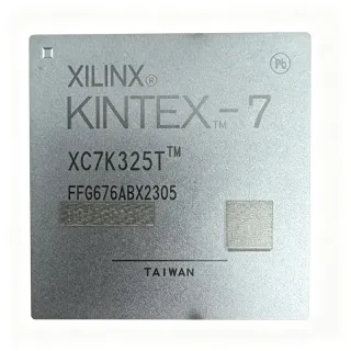
XC5VLX85-2FFG676C - 82,944-Cell Virtex-5 FPGA | AMD
MPN: XC5VLX85-2FFG676C ✗ Akhir HidupXC5VLX85-2FFG676C Ringkasan
A field-programmable gate array, or FPGA, is a programmable semiconductor in which configurable logic, block RAM, input/output resources, and dedicated hard processors are arranged into a device tailored for digital logic implementation. The Virtex-5 LX FPGA belongs to the FPGA & CPLD product hierarchy and combines high-density programmable logic with high-speed serial connectivity, general-purpose I/O, dedicated memory resources, and hardened processing capabilities. This combination makes the device suitable when designers need substantial parallel processing in one package rather than an assembly of discrete logic devices.
The XC5VLX85-2FFG676C provides 82,944 logic cells organized around 440 logical cells per slice. Its embedded memory totals 3.38 Mbit, enabling packet buffering, local storage, data acquisition, and display-processing functions without external memories. Additional hard resources include dedicated block RAM, DSP processing elements, input/output logic, clock management, and high-speed serial transceivers. These resources allow parallel video, communications, signal-processing, and industrial-control functions to be consolidated into a single FPGA implementation.
The 676-ball FCBGA package supports dense board routing and direct ball-grid-array assembly, but it requires a multilayer PCB with carefully controlled escape routing, power distribution, and thermal management. The -2 suffix identifies the device speed grade, while the C suffix identifies its commercial temperature designation. Green-package and industrial-temperature alternatives in the same Virtex-5 LX family can be considered when supply, qualification, or assembly requirements differ.
Typical uses include industrial automation, video processing, telecommunications, networking equipment, test and measurement systems, embedded control, and high-speed serial interface designs. The large logic and memory resources are especially valuable for parallel image pipelines, protocol conversion, real-time signal processing, and tightly coupled control systems that benefit from deterministic FPGA execution.
Designers should use the manufacturer pinout and package files when assigning every 676-ball position and should budget conservative fanout for I/O-heavy interfaces. A multilayer board should provide independent power and ground planes, short return paths, decoupling close to supply pins, and uninterrupted thermal paths. Configuration interfaces, clocking, memory migration, and high-speed differential routing must also be validated against the device documentation before layout release.
This product page combines the exact ordering information, package identity, logic and memory resources, documented equivalent devices, and engineering-oriented replacement guidance for faster component selection and PCB planning.
Alternatif penggantian untuk XC5VLX85-2FFG676C — paket yang sama, pin-pada-pin kompatibel. Bagian paket yang berbeda memerlukan kerja ulang PCB diabaikan.
Variasi di dalam seri ini
Model-series yang sama yang kompatibel dengan penggantian XC5VLX85-2FFG676C (sama faktor bentuk dan footprint) — berbeda di dalam Device Type, Programmable Logic Type, Logic Cells, Package, Core Supply Voltage.
XC5VLX85-2FFG676I
✅ Drop-InKontak untuk harga
Lihat Datasheet →XC5VLX85-2FF676I
✅ Drop-InKontak untuk harga
Lihat Datasheet →XC5VLX85-2FF676C
✅ Drop-In📋 Alternatif referensi (tidak dalam katalog)
XC5VLX85-2FFV676C
✅ Drop-In📋 Alternatif referensi (tidak dalam katalog)
XC5VLX85-2FFV676I
✅ Drop-In📋 Alternatif referensi (tidak dalam katalog)
XC5VLX85-2FFG676C Rating Maksimal & Karakteristik Listrik
| Device Type | Virtex-5 LX FPGA |
| FPGA Logic Cells | 82,944 cells |
| Logical Cells per Slice | 440 cells |
| Embedded Memory | 3.38 Mbit |
| Process Technology | 65 nm CMOS |
| Core Supply Voltage | 1 V |
| Speed Grade | -2 |
| Paket | 676-BBGA, FCBGA |
| Jumlah Pin | 676 balls |
| Tipe Mounting | Surface Mount |
| Programmable Logic Type | Field Programmable Gate Array |
| Manufacturer | AMD / Xilinx |
| Product Family | Virtex-5 LX |
XC5VLX85-2FFG676C 676-bbga, fcbga Diamant Konfigurasi Panduan
Konfigurasi pin untuk XC5VLX85-2FFG676C (676-bbga, fcbga pakai pakai). IC digital ini termasuk GPIO, antarmuka komunikasi (UART, SPI, I2C), dan pin kuasa. Lihat datasheet produsen untuk fungsi pin alternatif dan opsi konfigurasi. Penting untuk desain sistem pengemasan dan PCB.

Tidak ada data diatribut pin yang tersedia untuk XC5VLX85-2FFG676C.
Lihat ke: datasheet produk untuk konfigurasi pin penuh.
Aplikasi Umum
XC5VLX85-2FFG676C cocok untuk 6 aplikasis: Industrial Automation and Control, Video and Image Processing, Telecommunications and Network Equipment, Test and Measurement Systems, High-Speed Data Acquisition, Aerospace and Defense Legacy Systems.
Industrial Automation and Control
The XC5VLX85-2FFG676C fits factory-control designs that combine sequential control, communication interfaces, and real-time signal handling in one programmable device. Its 82,944 logic cells provide substantial parallel capacity, while 3.38 Mbit of embedded block RAM can support acquisition buffers, protocol state, and data history without immediate external-memory access. The -2 speed grade provides a performance-oriented Virtex-5 LX option, and the nominal 1 V core supply supports contemporary FPGA power architectures. For industrial deployment, confirm that the commercial temperature designation covers the enclosure temperature and use the 676-ball package files to preserve PCB compatibility during any alternate-source transition.
Direkomendasikan
Video and Image Processing
The XC5VLX85-2FFG676C is suitable for parallel video pipelines that require filtering, pixel transformation, color processing, and interface bridging. Its 82,944 logic cells can implement substantial fixed-function datapaths, and the 3.38 Mbit of block RAM is useful for line buffers, frame staging, and reusable lookup data. The dedicated DSP resources further support filtering and fixed-point arithmetic when enabled in the FPGA design. Because the device is surface-mounted in a 676-ball FCBGA, layout should minimize escape-routing congestion and provide continuous thermal paths for sustained image-processing workloads.
Direkomendasikan
Telecommunications and Network Equipment
The XC5VLX85-2FFG676C can support telecom and networking functions requiring parallel packet processing, high-speed serial links, and local buffering. The Virtex-5 LX feature set combines programmable logic, block RAM, DSP resources, clock management, and serial transceivers, allowing designers to consolidate framing, traffic management, and interface adaptation. Its 82,944 logic cells offer enough density for multiple parallel datapaths, while 3.38 Mbit of embedded memory can absorb short packet or timing queues. High-speed differential routes require controlled impedance, careful reference-plane continuity, and length matching based on the selected transceiver interfaces.
Direkomendasikan
Test and Measurement Systems
The XC5VLX85-2FFG676C fits modular test and measurement equipment where acquisition, timing, stimulus generation, and analysis need deterministic parallel execution. Its 82,944 logic cells allow multiple channels and control paths to operate concurrently, while 3.38 Mbit of embedded block RAM supports sample buffering and calibration tables. The -2 grade favors performance-sensitive measurement functions, and programmable I/O permits adaptation to different capture and trigger architectures. Because this is an obsolete device, new instrument platforms should also evaluate a currently supported FPGA, while legacy instruments can use the listed same-package equivalents for controlled maintenance programs.
Direkomendasikan
High-Speed Data Acquisition
The XC5VLX85-2FFG676C is appropriate for multi-channel acquisition systems that need parallel conversion, digital filtering, buffering, and data transfer. The FPGA's 82,944 logic cells support wide sampling networks and control sequences, while 3.38 Mbit of block RAM allows local storage of captured words before downstream processing. Its DSP resources can accelerate multiply-accumulate operations commonly used in digital signal conditioning. For a new acquisition platform, confirm converter timing compatibility, required I/O voltage standards, and thermal margins; for an existing design, preserve the 676-ball footprint and verify the selected alternate's complete ordering attributes.
Direkomendasikan
Aerospace and Defense Legacy Systems
The XC5VLX85-2FFG676C may be used in legacy aerospace, defense, or other mission-critical equipment where a programmed Virtex-5 LX design and qualified manufacturing flow already exist. Its 82,944 logic cells support complex control, navigation, signal-processing, and redundancy functions, while 3.38 Mbit of embedded memory provides local data storage. Qualification status for a particular aerospace or defense role is not established by the ordering code alone and must be confirmed through program-specific records. Because the FPGA family is obsolete, sustaining deployments should carefully control substitutions, inspect traceability, and verify configuration compatibility before introducing any alternate MPN.
Direkomendasikan
Ringkasan Produk Direkomendasikan
Data referensi engineering untuk XC5VLX85-2FFG676C — pembandingan, panduan desain, dan informasi konformitas.
Panduan Pemilihan
Pembandingan dengan Alternatif
| Parameter Umum | Produk Ini | XC5VLX85-2FFG676I | XC5VLX85-2FF676I | XC5VLX85-2FF676C | XC5VLX85-2FFV676C | XC5VLX85-2FFV676I |
|---|---|---|---|---|---|---|
| Package | 676-BBGA, FCBGA | 676-BBGA, FCBGA | 676-BBGA, FCBGA | 676-BBGA, FCBGA | 676-BBGA, FCBGA | 676-BBGA, FCBGA |
| Brand | AMD / Xilinx | AMD / Xilinx | AMD / Xilinx | AMD / Xilinx | AMD / Xilinx | AMD / Xilinx |
| FPGA Family | Virtex-5 LX | Virtex-5 LX | Virtex-5 LX | Virtex-5 LX | Virtex-5 LX | Virtex-5 LX |
| FPGA Logic Cells | 82,944 cells | 82,944 cells | 82,944 cells | 82,944 cells | 82,944 cells | 82,944 cells |
| Logical Cells per Slice | 440 cells | 440 cells | 440 cells | 440 cells | 440 cells | 440 cells |
| Embedded Memory | 3.38 Mbit | 3.38 Mbit | 3.38 Mbit | 3.38 Mbit | 3.38 Mbit | 3.38 Mbit |
| Process Technology | 65 nm CMOS | 65 nm CMOS | 65 nm CMOS | 65 nm CMOS | 65 nm CMOS | 65 nm CMOS |
| Core Supply Voltage | 1 V | 1 V | 1 V | 1 V | 1 V | 1 V |
| Speed Grade | -2 | -2 | -2 | -2 | -2 | -2 |
| Temperature Ordering Option | Commercial C suffix | Industrial I suffix | Industrial I suffix | Commercial C suffix | Commercial C suffix | Industrial I suffix |
Diferensiator Kunci
- Direct commercial-grade ordering option (vsXC5VLX85-2FFG676I)
- Same density and embedded memory in the core replacement family (vsXC5VLX85-2FF676C)
- Same performance grade with an alternate package code (vsXC5VLX85-2FFV676C)
- Full 676-ball integration for high-density parallel designs (vsXC5VLX85-2FFV676I)
Catatan Desain
Use the AMD Virtex-5 package pinout files and manufacturer land pattern to verify all 676 ball assignments before routing. Create independent core, auxiliary, and I/O supply paths where the pinout permits separation, then connect them through plane or high-frequency distribution structures. Place bulk and local decoupling according to the device guidance, maintain short ground-via paths, and preserve uninterrupted copper beneath the BGA for thermal conduction.
The exact power budget depends on configuration, clocking, I/O activity, and resource utilization, so calculate it with the device power-estimation flow for the final design. A 65 nm FPGA can still dissipate substantial power in a dense 676-ball FCBGA when many logic, DSP, memory, and serial blocks are active. Validate junction-temperature margin at the highest ambient temperature and use thermal vias, solid plane layers, enclosure airflow, or a heat spreader as required.
Route high-speed serial and clock signals over continuous reference planes with controlled impedance, and match differential pairs according to the selected interface constraints. Keep configuration pins and their pull networks away from aggressive switching nodes. Avoid vias in sensitive high-speed escape paths where possible, and avoid splitting return paths beneath the FPGA. Validate escape-routing topology and layer transitions against the exact 676-ball package rather than a generic BGA layout.
Do not approve an alternate solely because its family name and package look similar. Confirm the complete ordering suffix, temperature option, package markings, pinout, footprint, configuration compatibility, and qualification requirements. Also verify that the replacement supports every bitstream feature and I/O standard used by the design. For an obsolete FPGA, preserve the original part number, lot traceability, firmware images, and test documentation to reduce maintenance risk.
Informasi Konformitas
The FFG suffix indicates a green-package ordering option, but formal RoHS, REACH, halogen-free, and conflict-minerals compliance cannot be established from the ordering information alone. Automotive or aerospace qualification must be confirmed through program-specific records.