ADC/DAC
製品 (2398)

MAX187CCWE - 12-Bit 75kSPS Serial ADC | Maxim Integrated
The Maxim Integrated MAX187CCWE is a +5V, low-power, 12-bit serial successive-approximation analog-to-digital converter (SAR ADC) in a 16-pin SOIC wide package. It integrates an 8.5 us SAR core, a 1.5 us track/hold amplifier, an on-chip clock, and a high-speed 3-wire serial interface, accepting a single-ended 0V to 5V analog input. An SAR ADC is a type of analog-to-digital converter that uses a binary-search successive-approximation algorithm against an internal DAC to digitize an analog input one bit per clock cycle. SAR ADCs sit in the broader hierarchy of precision data converters -> ADCs -> successive-approximation ADCs -> integrated-circuit semiconductor. Compared with integrating or delta-sigma ADCs, SAR ADCs deliver the best combination of speed and accuracy for multiplexed or single-channel industrial sampling up to a few hundred kilosamples per second. Key features of the MAX187CCWE include 75 kSPS sampling rate, internal 4.096V reference, 1.5 us acquisition time, 8.5 us conversion time, low 1.5 mA operating supply current, and hardware- or software-configurable shutdown reducing quiescent current to a few microamps. The internal reference eliminates an external reference IC in many designs, saving board area and BOM cost. The MAX187CCWE uses a charge-redistribution SAR architecture with an internal capacitor DAC and a precision internal bandgap reference. Its high-speed serial interface is compatible with SPI, QSPI, and Microwire, allowing direct connection to most microcontrollers without glue logic. Internal calibration trims linearity, and the device maintains 12-bit performance across the commercial 0C to +70C temperature range. Typical applications include portable data logging, process control, pen digitizers, portable instruments, isolated data acquisition, and remote-sensor signal conditioning. The wide operating supply range and serial interface make it ideal for compact, low-power embedded designs where a microcontroller-based SPI host is already present. When designing with the MAX187CCWE, ensure the analog input does not exceed VDD + 0.3V to avoid latch-up. Place a 0.1 uF bypass capacitor close to the supply pin and keep analog traces short to minimize digital-noise coupling into the high-impedance input. This page synthesizes distributor pricing, drop-in alternatives within the MAX187 family, and practical design notes not found in the manufacturer datasheet alone.

MAX187CEPA - 12-Bit Serial ADC, +5V, 75ksps, DIP-8 | Maxim
The Maxim Integrated (now Analog Devices) MAX187CEPA is a +5V, low-power, 12-bit serial analog-to-digital converter (ADC) housed in an 8-pin PDIP (DIP-8) package. It accepts a 0V to 5V analog input, integrates a successive-approximation ADC with 8.5us conversion time, a 1.5us track/hold, an on-chip clock, and a high-speed 3-wire SPI/QSPI/MICROWIRE-compatible serial interface. An internal 4.096V buffered reference simplifies external circuitry and removes the need for a separate reference IC in most applications. An ADC (analog-to-digital converter) is a mixed-signal data-acquisition component that samples a continuous analog voltage and quantizes it into a discrete digital code. Within the power management and signal-chain hierarchy, ADCs sit downstream of analog signal conditioning (op-amps, filters) and upstream of microcontrollers, DSPs, or FPGAs. The MAX187 family belongs to the successive-approximation register (SAR) ADC category, which trades conversion speed for excellent static accuracy and low power consumption, making it a workhorse for industrial process control, instrumentation, and portable data-logger designs. Key specifications include 12-bit resolution, +/-0.5 LSB integral nonlinearity (INL) for the MAX187A grade, 75kHz (75ksps) sampling rate, 1.5mA operating supply current, and a 2uA shutdown current that lets battery-powered systems gate power between conversions. The MAX187 variant includes the internal 4.096V reference; the pin-compatible MAX189 leaves REF open for an external reference. Internal calibration circuitry holds linearity over the full operating temperature range. Typical applications include portable instrumentation, data loggers, process-control analog front ends, weigh scales, isolated sensor digitizers, and pen-digitizer / tablet digitizing systems. The wide analog input range (0 to 5V) plus internal reference make it a single-chip solution for many industrial 4-20mA loop and thermocouple-amplifier digitizing tasks. When designing with the MAX187CEPA, place 0.1uF decoupling close to VDD and follow the recommended REF bypass (4.7uF) to keep the internal reference quiet. Use the SHDN pin aggressively in battery systems - the 2uA quiescent current drops total system standby power dramatically versus always-on operation. This page synthesizes distributor pricing, pin-compatible drop-in alternatives (MAX187BEPA, MAX187ACPA+, MAX187CCPA+), and practical design notes not consolidated in the manufacturer datasheet, enabling faster engineering decisions.
MAX187CEWE - 12-Bit 75kSPS Serial ADC, 16-SOIC | Maxim Integrated
The Maxim Integrated MAX187CEWE is a +5V, low-power, 12-bit successive-approximation analog-to-digital converter (SAR ADC) with an on-chip buffered reference, packaged in a 16-pin SOIC (wide-body, "WE") and rated for the extended industrial temperature range (C: -40°C to +85°C). It accepts a single-ended analog input from 0V to +5V and serializes conversion results over an SPI/QSPI/MICROWIRE-compatible interface at throughput up to 75k samples per second. According to the manufacturer datasheet, the part consumes only 7.5 mW during continuous conversion and drops to 10 µW in hardware shutdown, making it appropriate for battery and loop-powered instrumentation where thermal budget and quiescent draw matter. An ADC of this type is a mixed-signal data converter that digitizes a continuously variable analog voltage into a fixed-width binary code; the MAX187CEWE specifically uses a successive-approximation architecture, where an internal DAC and comparator walk through 12 bits one at a time per conversion. Within the converter hierarchy, the MAX187CEWE belongs to the SAR ADC sub-family of precision converters, which in turn sits under the broader ADC/DAC product category and the integrated-circuits family. SAR ADCs are favored when designers need deterministic latency, low latency per sample, good DC linearity, and simple serial interfacing — they are common in industrial process control, instrumentation, sensor read-out, and portable measurement front-ends where the alternative delta-sigma and pipeline architectures either burn more current or carry longer pipeline delays. Key specifications include 12-bit resolution, 75 kSPS maximum sampling rate, an 8.5 µs successive-approximation conversion time, a 1.5 µs acquisition track/hold, and ±1 LSB maximum integral nonlinearity. Power operation is single +5 V supply (specified 4.75 V to 5.25 V) with 1.5 mA operating supply current and 10 µA shutdown current; the internal reference is a low-drift 4.096 V bandgap. The 16-pin SOIC "WE" package gives a 0.300" wide-body outline with a thermal-resistance profile typical of plastic SO. Typical applications span 4–20 mA loop-powered sensor transmitters, pen-tablet/stylus digitizers, portable data loggers, isolated analog-input modules, and front-end digitizers for microcontrollers that lack on-board ADCs of adequate precision. For each, the MAX187CEWE's 5 V single-supply operation, internal reference and tight INL simplify the analog front end by eliminating external reference and negative-rail circuitry. When designing with this converter, follow the recommended supply decoupling scheme (4.7 µF + 0.1 µF) and keep analog/digital grounds star-routed to the MAX187CEWE GND pin to preserve the 12-bit linearity. Where lower supply operation or higher throughput is needed, evaluate the MAX1240 (3 V variant) and MAX189 (external-reference variant) — see the comparison table. This page synthesizes distributor pricing for the bare "CEWE" (no +, non-compliant suffix) variant, drop-in alternatives also sourced from Maxim's own MAX187 family, and practical design notes that are not duplicated verbatim from the manufacturer datasheet.

MAX188BEPP - 12-Bit 8-Ch 133ksps Serial ADC | Maxim Integrated
The Maxim Integrated MAX188BEPP is a low-power, 8-channel, 133 ksps, serial 12-bit analog-to-digital converter (ADC) with internal track/hold and reference, housed in a 20-pin PDIP package. It features 8 single-ended or 4 differential analog input channels, an internal 4.096 V reference, and an SPI/QSPI/Microwire-compatible serial interface that simplifies connection to most microcontrollers and DSPs. A successive-approximation ADC (SAR ADC) is a type of data converter that converts an analog input signal into a digital code by performing a binary search across an internal precision resistor ladder. SAR ADCs are valued for their deterministic latency, lack of pipeline delay, and excellent DC accuracy, making them the converter of choice for multiplexed data-acquisition front-ends, industrial process control loops, sensor signal chains, and instrumentation. Within the broader semiconductor taxonomy, the MAX188 sits in the data-acquisition IC category, adjacent to DACs, analog front-ends, and precision reference ICs. Key features of the MAX188BEPP include 133 kHz sampling rate, single +5 V or dual ±5 V supply operation, low operating current of 1.5 mA and an ultra-low 2 µA power-down current, ±5 V input range for bipolar signal acquisition, internal track/hold, and 4-wire serial output. The device accepts unipolar or bipolar analog inputs, providing flexible signal-conditioning headroom for transducer bridge circuits, thermocouple amplifiers, and 4-20 mA current-loop receivers. Architecturally, the MAX188 integrates an 8-channel analog multiplexer, a high-bandwidth track/hold, a precision 4.096 V internal reference, a 12-bit successive-approximation ADC core, and an SPI-compatible digital interface on a single die. The internal reference eliminates external reference cost and PC board area while delivering tight full-scale accuracy. The high-bandwidth track/hold captures fast-moving signals, and the 8-channel mux removes the need for external analog switches in multi-sensor systems. Typical applications for the MAX188BEPP include industrial process control, portable data-logging instruments, battery-powered sensor nodes, medical instrumentation front-ends, factory automation I/O modules, and distributed SCADA analog input cards. The 133 ksps throughput is well matched to multiplexing several channels of slowly-varying process signals. When designing with this ADC, place a 0.1 µF bypass capacitor as close as possible to the VDD pin, and provide adequate analog/digital ground separation with a single-point star connection near the IC. The internal reference requires a minimum 4.7 µF bypass capacitor on the REF pin for stable full-scale accuracy; omitting this degrades linearity. This page synthesizes distributor stock levels, drop-in alternatives, and practical design guidance that the bare datasheet does not provide, helping engineers shorten time-to-prototype for their 12-bit data-acquisition front-end.

MAX189BC/D - 12-Bit SAR ADC, Serial, 75ksps | Maxim Integrated
The Maxim Integrated MAX189BC/D is a 12-bit, low-power, serial-output, successive-approximation analog-to-digital converter (SAR ADC) supplied as a bare die (D suffix). It operates from a single +5V supply, accepts a 0V to 5V analog input range, and includes an internal track/hold, an internal 4.096V buffered reference, and a 3-wire SPI/QSPI/MICROWIRE-compatible serial interface. The MAX189BC/D performs conversions in approximately 8.5 microseconds and supports a maximum throughput of 75 kilosamples per second (ksps). A SAR ADC (Successive Approximation Register Analog-to-Digital Converter) is a type of ADC that converts an analog input to a digital output using a binary-search algorithm against an internal DAC. SAR ADCs balance conversion speed, power consumption, and resolution, making them the workhorse of medium-speed data-acquisition applications such as industrial sensors, handheld instruments, and process-control front-ends. In the broader IC taxonomy, an SAR ADC sits under Data Converters -> ADCs -> Medium-Speed ADCs -> Power-Efficient ADCs. Key features of the MAX189BC/D include +/- 1/2 LSB integral nonlinearity (INL), a fast 1.5-microsecond acquisition-time track/hold, an internal 4.096V reference that can also drive external loads, a hardware- or software-controllable shutdown mode that drops supply current to 2 microamps, and 1.5 mA operating current. The serial interface is compatible with SPI, QSPI, and MICROWIRE, easing connection to most modern microcontrollers and DSPs without external glue logic. The MAX189BC/D's architecture uses a capacitive-charge-distribution DAC at its core, with a precision comparator and SAR logic, plus an integrated reference and reference buffer. The "C" speed grade and "B" resolution grade (with +/- 1 LSB INL vs. the A grade +/- 1/2 LSB) make the BC variant an attractive cost-optimized option. The bare-die format allows hybrid-module integrators and MCM (multi-chip-module) designers to minimize parasitic inductance and shrink board area beyond what packaged parts permit. Typical applications include portable data loggers, pen-tablet digitizers, battery-powered instrumentation, isolated sensor read-out stages, and industrial process-control front-ends. The combination of a single +5V supply, low power, and serial output suits distributed measurement nodes and space-constrained designs. When designing with the MAX189BC/D, provide a clean analog ground plane separate from the noisy digital return, bypass VDD with a 0.1 microfarat ceramic close to each die supply bond, and use the SHDN pin for duty-cycling to extend battery life. The internal reference can source up to several hundred microamps; if your design also needs a reference for external ADCs, budget that current draw into the worst-case accuracy calculation. This page synthesizes distributor pricing, pin-compatible alternatives, and practical design notes not found in the manufacturer datasheet.
MAX189BEPA+ - 12-Bit Serial ADC, +5V, 75kSPS | Maxim Integrated
The Analog Devices (formerly Maxim Integrated) MAX189BEPA+ is a 12-bit, low-power, serial-output successive-approximation analog-to-digital converter (ADC) operating from a single +5V supply, housed in an 8-pin PDIP package. It accepts a 0V to 5V analog input range, includes an internal track/hold with 1.5us acquisition time, and provides a high-speed 3-wire SPI/QSPI/MICROWIRE-compatible serial interface. The device supports a 75 kHz sampling rate with 8.5us conversion time, drawing only 1.5 mA operating current and dropping to 2uA in shutdown mode. A successive-approximation register (SAR) ADC is a type of analog-to-digital converter that uses a binary search algorithm and an internal capacitive DAC to convert each analog sample in a fixed number of clock cycles. SAR ADCs offer deterministic latency, no-pipeline delay, and excellent dynamic performance at moderate sampling rates, making them ideal for multiplexed data acquisition, industrial process control, and instrumentation. The MAX189 belongs to the data converter family within precision analog signal-chain ICs, ranking alongside delta-sigma and pipeline ADCs in the precision measurement hierarchy. Key features include +/-1/2 LSB integral nonlinearity (A-grade), 75 kHz throughput, internal 4.096V buffered reference on the MAX187 (external reference required on the MAX189), and a hardware/software shutdown mode that reduces supply current to 2uA. The external-reference architecture of the MAX189 lets designers connect a precision reference for ratiometric or higher-accuracy applications, while the MAX187 variant provides an internal reference for minimum external parts count. Typical applications include data logging, process control, isolated data acquisition, battery-powered instrumentation, and pen-digitizer digitizing tablets. The wide supply tolerance of 4.75V to 5.25V and -40C to +85C industrial temperature range make it suitable for harsh embedded environments where thermal and supply variation would otherwise degrade accuracy. When designing with the MAX189, place the external reference bypass capacitor (4.7uF minimum) close to the REF pin and keep the analog input traces short and guarded. For best noise performance, use an external reference such as the MAX6141 or MAX6250 with 4.096V output to match the input span. This page synthesizes distributor pricing, verified drop-in alternatives (same-brand MAX187/MAX176 family first, then pin-compatible cross-brand 12-bit SAR ADCs), and practical design notes not consolidated on the manufacturer datasheet.

MAX190ACWG - 12-Bit 75ksps SAR ADC, SOIC-24 | Analog Devices
The Analog Devices (formerly Maxim Integrated) MAX190ACWG is a low-power, 12-bit sampling analog-to-digital converter (ADC) with internal reference and power-down capability, housed in a 24-pin wide SOIC (WG) package. It delivers up to 75 ksps throughput from a single +5V analog supply, drawing only 3 mA quiescent current during conversion and dropping to 60 µA in software-controlled power-down mode. The device integrates an internal 4.096V bandgap reference, a successive-approximation register (SAR) architecture, and an on-chip sample-and-hold amplifier. An ADC (Analog-to-Digital Converter) is a data-acquisition component that converts continuous analog signals into discrete digital codes. The MAX190 belongs to the SAR (Successive Approximation Register) family of ADCs, which sit in the broader hierarchy: SAR ADC -> data converter -> ADC/DAC -> signal-chain IC -> semiconductor. SAR ADCs offer a strong balance of speed, resolution, and power for multiplexed or single-channel precision measurement in industrial, instrumentation, and process-control systems. Key features of the MAX190ACWG include ±0.5 LSB integral nonlinearity (INL) in the A-grade, internal low-drift reference, software-configurable unipolar (0 to +5V) or bipolar (±5V) analog input range, and a Byte-wide parallel data interface. The device requires an external 2.5 MHz to 5 MHz serial clock, and its 100 ns acquisition time supports full 75 ksps conversion throughput on a single acquisition/conversion cycle. The integrated reference eliminates the need for external precision components, reducing BOM cost and PCB area. Typical applications include data-logging systems, pen digitizers, portable instrumentation, industrial process control, and battery-powered measurement equipment where the 60 µA power-down mode significantly extends battery life. The MAX190ACWG is the commercial temperature grade (0°C to +70°C), while the MAX190AEWG is the extended temperature grade (−40°C to +85°C) for harsher environments. Designers should add a 10 µF bypass capacitor on the analog supply and follow standard ADC layout practices — keep analog and digital ground planes separate and connect them only at a single point near the IC. This page synthesizes distributor pricing, drop-in alternatives, and practical design notes not found in the manufacturer datasheet alone, helping engineers evaluate the MAX190ACWG for both new designs and legacy maintenance.
MAX190BCWG+T - 12-Bit 75ksps SAR ADC w/ Ref | Maxim Integrated
The Maxim Integrated MAX190BCWG+T is a 12-bit, low-power, successive-approximation analog-to-digital converter (SAR ADC) with an internal 2.5V reference, an on-chip track-and-hold, and a hardware power-down mode, housed in a 24-pin wide-body SOIC package. It supports a 75 ksps sampling rate on a single +5V analog supply (with an optional +5V digital supply) and offers both serial and parallel (8-bit bus) digital interfaces for design flexibility. An SAR ADC is a successive-approximation-register analog-to-digital converter, a category of precision data converter that uses an internal binary-search algorithm and a precision DAC to convert an analog input to a digital code in N clock cycles (N = resolution in bits). SAR ADCs sit in the broader hierarchy of data converters alongside flash, pipelined, sigma-delta, and dual-slope ADCs, and are valued for their excellent DC accuracy, deterministic latency, and low power consumption in multiplexed data-acquisition systems. The MAX190BCWG+T integrates a 2.5V buried-zener reference (typically 50 ppm/°C drift), an analog input track-and-hold rated for signals up to ±VREF, and 8 software-selectable input ranges. Key specifications include ±0.5 LSB (max) integral nonlinearity (B-grade), ±2 LSB (max) gain error, ±2 LSB (max) offset error, and a SINAD of 70 dB. Power consumption is approximately 5 mW active and under 10 µW in shutdown, while the serial interface supports SPI/QSPI/MICROWIRE-compatible mode 0 communication. The device uses a charge-redistribution DAC architecture with a binary-weighted capacitor array and on-chip calibration logic that corrects linearity errors on power-up. The MAX190BCWG+T operates over the commercial 0°C to +70°C range and uses an external reference capacitor (4.7 µF) on the REF pin for noise filtering; a fully internal reference mode is available when the user-supplied reference is bypassed. Typical applications include portable data loggers, battery-powered instrumentation, industrial process control loops, pen-tablet digitizers, and isolated-sensor signal conditioning. Its low active power and sub-10 µW shutdown make it ideal for solar- or battery-powered remote telemetry endpoints where idle current dominates system energy budget. When designing with the MAX190BCWG+T, the 4.7 µF reference capacitor, 10 µF input-coupling RC network, and quiet +5V analog supply layout are critical for achieving datasheet AC performance. For highest accuracy, use the A-grade (MAX190ACWG+) variant; the B-grade (this part) trades linearity for lower cost. The serial-mode pinout simplifies isolated signal chains because only four digital lines cross the isolation barrier. This page synthesizes distributor pricing from DigiKey, Mouser, and Octopart, drop-in and pin-compatible alternatives (MAX190ACWG+, MAX190AEWG+, MAX190BEWG+, etc.), and practical design notes not consolidated in the manufacturer datasheet.

MAX19192ETI/V+ - 10Msps Dual 8-Bit Ultra-Low-Power ADC | Maxim
The Maxim Integrated (now Analog Devices) MAX19192ETI/V+ is an ultra-low-power, dual-channel, 8-bit analog-to-digital converter (ADC) capable of 10Msps sampling rate per channel, housed in a 28-pin thin QFN (TQFN) package measuring 5 mm x 5 mm. The device features two fully differential wideband track-and-hold (T/H) front ends with 440 MHz input bandwidth, supporting both fully differential and single-ended input signals. Typical signal-to-noise-plus-distortion (SINAD) is 48.6 dB at a 1 MHz analog input frequency, with spurious-free dynamic range (SFDR) performance suitable for mid-tier communications and instrumentation. An ADC (Analog-to-Digital Converter) is a mixed-signal integrated circuit that samples continuous analog voltage levels and converts them into discrete digital codes. Within the broader semiconductor taxonomy, ADCs belong to the data converter family, which sits under signal chain ICs and ultimately under power management and analog mixed-signal semiconductors. The MAX19192's dual-channel, low-power architecture positions it in the pipeline/flash converter category, optimized for simultaneous sampling of two correlated signals without channel-to-channel skew penalty beyond the T/H aperture. Key features include 10 Msps sampling per channel, dual differential T/H inputs, 48.6 dB SINAD at fIN = 1 MHz, ultra-low power consumption (well below 30 mW total at full speed), and a parallel digital output interface. The 440 MHz T/H bandwidth supports undersampling of IF signals, while the extended industrial -40C to +85C operating temperature range allows deployment in harsh environments without derating. The 28-pin TQFN package provides a compact footprint suitable for portable, space-constrained designs. The MAX19192 architecture combines a flash-style quantization core with high-bandwidth T/H input stages, enabling low-latency conversion with deterministic aperture delay. The differential input structure rejects common-mode noise, which is critical when digitizing small signals in the presence of digital switching noise on the same PCB. Internal reference and clock buffering simplify external BOM. Typical applications include portable ultrasound imaging front ends, low-power communication baseband digitizers, handheld oscilloscope input stages, I/Q demodulator outputs in software-defined radio, dual-antenna diversity receivers, and industrial data acquisition modules where two correlated analog signals must be captured simultaneously. When designing with this device, allocate adequate PCB area for the exposed thermal pad to maintain theta_JA performance, and keep analog and digital ground returns separated until they join at the IC's GND pin to avoid coupling digital switching noise into the analog input path.
MAX191BC/D - 12-Bit 100ksps SAR ADC w/ Internal Ref | Maxim
The Maxim Integrated MAX191BC/D is a monolithic CMOS 12-bit analog-to-digital converter (ADC) featuring differential inputs, on-chip track/hold, internal 4.096V voltage reference, internal or external clock, and parallel or serial microprocessor interface. It delivers a 7.5us conversion time and a 2us acquisition time, guaranteeing a 100ksps sample rate. The MAX191BC/D is supplied as bare die (/D suffix), targeting compact hybrid assemblies and multi-chip modules where the converter is bonded directly inside the package. An SAR (Successive Approximation Register) ADC is a type of data converter that resolves one bit per clock cycle by comparing the sampled input against a precision DAC driven by a binary-weighted register. SAR ADCs combine high accuracy (typically 12-18 bits), zero pipeline latency, and excellent DC input behavior, making them the architecture of choice for multiplexed data acquisition systems, precision instrumentation, and process-control front-ends. Within the broader taxonomy, the SAR sits between flash converters (faster, lower resolution) and delta-sigma converters (slower, higher resolution). Key features of the MAX191BC/D include 12-bit resolution with 1/2 LSB linearity at +/-5V operation, a built-in track/hold, an adjustable internal reference, low power consumption of 3mA in operating mode and 20uA in power-down, and a logic-level PWRDN input. It accepts single +5V or dual +/-5V supplies, allowing ground-referenced bipolar inputs of up to +/-5V. The part uses a SAR core with internal calibration logic for excellent linearity without external trimming. The MAX191 is most commonly used in high-accuracy data-acquisition boards, industrial process control, battery-powered portable instrumentation, and pen-digitizer/sensor signal chains. The wide bipolar input range simplifies signal conditioning when measuring ground-referenced signals. The low 20uA power-down current extends battery life in duty-cycled portable systems, and the die form factor minimizes PCB area. When designing with the MAX191BC/D, observe proper die-handling and ESD procedures because the bare die is exposed. Use a low-impedance analog ground plane and decouple AVDD/DVDD with separate 0.1uF/10uF capacitors placed within 5mm of the bond pads. The internal reference may be overdriven with an external 4.096V source if higher accuracy or lower drift is required. This page synthesizes distributor pricing, drop-in alternatives, and practical design notes not found in the manufacturer datasheet alone, helping engineers accelerate their selection and PCB-layout decisions for new designs and MAX191BC/D replacements.

MAX191BCNG - 12-Bit 100kSPS Sampling ADC, 24-PDIP | Maxim Integrated
The Analog Devices (formerly Maxim Integrated) MAX191BCNG is a low-power, monolithic CMOS 12-bit analog-to-digital converter (ADC) with differential inputs, built-in track/hold (T/H), an internal voltage reference, and a parallel microprocessor interface. Housed in a 24-pin PDIP (N) package, the part delivers a 7.5 us conversion time, 2 us acquisition time, and a guaranteed 100 kSPS sample rate from a single +5 V (or +/-5 V) supply while drawing only 3 mA in operating mode and 20 uA in power-down. An ADC (analog-to-digital converter) is a data converter that transforms continuous analog voltages into discrete digital codes for processing by microcontrollers, DSPs, or FPGAs. Successive-approximation-register (SAR) ADCs like the MAX191 use a binary-search algorithm to resolve N bits in N clock cycles, making them well-suited for multiplexed data-acquisition systems, instrumentation, and process control where moderate speed and high accuracy are required. Within the broader converter hierarchy, the MAX191 sits between 8/10-bit SAR parts and higher-resolution 14-16-bit SAR or delta-sigma converters, offering a balanced trade-off of speed, accuracy, and power for industrial and instrumentation applications. Key features of the MAX191BCNG include +/-1/2 LSB linearity (B-grade), differential analog inputs, software-configurable unipolar/bipolar input ranges (0 V to +5 V or +/-5 V), an internal 2.5 V bandgap reference with adjustment capability, and a hardware power-down pin that reduces supply current to 20 uA between conversions. The parallel interface is directly compatible with most 8-bit microcontrollers and DSPs without external glue logic, and the internal reference eliminates the cost and board area of an external reference IC. Architecture is a classic charge-redistribution SAR with an auto-calibrated CMOS capacitor DAC and switched-capacitor T/H. The combination of low 3 mA operating current, 20 uA power-down, and 100 kSPS throughput makes the device one of the lowest-power 12-bit, 100 kSPS ADCs of its era, suitable for battery-powered and thermally-constrained designs. The 24-pin PDIP through-hole package simplifies prototyping, repair, and high-voltage bench-instrument front-ends where surface-mount parts are inconvenient. Typical applications include digital signal processing, precision industrial process control, microprocessor-based instrumentation, and portable/battery-powered data loggers where the 20 uA power-down mode extends battery life between conversions. Designers also use the MAX191 in pen-tablet digitizers and pin-compatible upgrades to earlier 12-bit PDIP ADCs. When designing with this part, ensure the analog input common-mode voltage stays within the specified range and place a 0.1 uF ceramic bypass capacitor as close as possible to the +V DD and +V SS pins to suppress digital switching noise. The internal reference should be decoupled with 4.7 uF tantalum plus 0.1 uF ceramic to achieve the datasheet's 1/2 LSB linearity at full 100 kSPS throughput. This page synthesizes distributor pricing, drop-in alternative MPNs sourced from cross-reference databases, and practical design notes that are not aggregated on a single manufacturer or distributor page.
MAX191BCWG-T - 12-Bit 75ksps Sampling ADC w/ Internal Ref | Maxim
The Maxim Integrated (Analog Devices / Maxim Integrated) MAX191BCWG-T is a 12-bit, low-power, sampling analog-to-digital converter (ADC) with an internal 4.096V bandgap reference and integrated power-down mode, housed in a 24-pin wide-body SOIC (WSOIC-24) package. It uses a successive-approximation register (SAR) architecture with an input track/hold to deliver up to 75 ksps throughput while consuming only 3 mA in normal operation and dropping to under 10 uA in shutdown. What is an SAR ADC? A successive-approximation-register analog-to-digital converter is a class of medium-speed, medium-resolution data converter that resolves one bit per clock cycle using an internal DAC, comparator, and SAR logic. SAR ADCs sit in the hierarchy: ADC -> data converter -> data acquisition IC -> mixed-signal semiconductor. Unlike delta-sigma ADCs they offer single-cycle conversions and excellent DC accuracy, and unlike flash ADCs they consume far less silicon area, making them ideal for multiplexed industrial and instrumentation channels. Key features of the MAX191BCWG-T include 12-bit resolution with no missing codes, an internal buried-Zener reference trimmed to within ±1.5%, a software-configurable analog input range of 0V to VREF or bipolar ±VREF, a Byte/parallel interface, and a hardware-active-low RD and CS control. The wide-body SOIC-24 package offers easy hand-soldering and straightforward prototype rework while still being surface-mountable for production. The internal reference removes the need for an external reference IC, saving PCB area and BOM cost in space-constrained designs. The MAX191 is built on a BiCMOS process that combines bipolar precision (for the bandgap reference and comparator) with CMOS logic for low-power digital control. This mixed-signal architecture gives the part a true DC accuracy better than ±1 LSB INL and DNL and a SINAD of approximately 70 dB, suitable for instrumentation, process control, and pen-digitizer front ends. Power-down is invoked by a single serial or parallel-mode command and is hardware-assertable through the active-low shutdown pin in the WSOIC package. Typical applications include data-logging front ends, pen-tablet digitizers, process-control analog input modules, portable instrumentation, and battery-powered data-acquisition boards. The combination of internal reference, single +5V supply operation, and low power-down current makes the part especially attractive for hand-held and remote-monitoring equipment. When designing with this part, allocate an input RC network (typically 1 kohm + 100 pF) to limit transients at the analog input, and route the VREF decoupling capacitor (4.7 uF minimum) as close to the REF pin as possible. Verify that the bipolar/unipolar mode jumper is correctly configured before sampling; otherwise conversions will be off-scale. This page synthesizes distributor pricing, obsolete-lifecycle sourcing guidance, same-brand replacements and cross-brand pin-to-pin ADC equivalents not found in the manufacturer datasheet alone.
MAX191BEWG - 12-Bit 100kSPS SAR ADC, SOIC-24 | Maxim
The Maxim Integrated (Analog Devices) MAX191BEWG is a low-power, 12-bit sampling analog-to-digital converter (ADC) featuring differential inputs, an internal 2.5V reference, track-and-hold (T/H), internal/external clock, and a parallel/serial microprocessor interface, all housed in a 24-pin wide SOIC (WSOIC-24 / EWG) package. Operating from a single +5V analog supply with ±5V input range, the part guarantees 100kSPS throughput via 7.5µs conversion plus 2µs acquisition timing, drawing only 3.0 mA active and 1µA in power-down. Built on a monolithic CMOS process, the successive-approximation architecture delivers ±0.5 LSB INL (B-grade) while providing flexible digital interfacing for μP, DSP, or direct data-bus connection. An ADC (analog-to-digital converter) is a data-acquisition IC that converts real-world analog signals into discrete digital codes usable by microcontrollers, DSPs, or FPGAs. The successive-approximation register (SAR) topology is the most common precision topology: it uses an internal comparator and a binary-weighted capacitor DAC to converge on the input voltage in N clock cycles for an N-bit result. SAR ADCs sit at the precision/throughput middle of the ADC family hierarchy, below delta-sigma (highest resolution, lowest speed) and above flash ADCs (fastest, lowest resolution). Key differentiating specifications include ±0.5 LSB integral non-linearity, no missing codes over the full -40°C to +85°C industrial range, and a hardware + software configurable power-down mode that drops supply current to 1µA for battery-aware applications. The internal buried-zener reference eliminates external reference components while maintaining low drift across temperature. Typical applications include data-acquisition front ends, pen digitizers, portable instrumentation, DSP analog input stages, and process-control I/O subsystems. The wide ±5V true bipolar input range (when using a separate -5V supply) or 0 to +5V unipolar range (single +5V supply) lets the part interface directly to industrial ±5V transducers and 4-20mA loops after resistor scaling. When designing with the MAX191BEWG, bypass VDD with a 10µF tantalum plus 0.1µF ceramic at the pin, place AGND and DGND on a single-star ground, and drive SHDN low only after clocks stabilize. For new designs, Analog Devices recommends the MAX129x family as the modern lower-power successor.

MAX192ACAP - 10-Bit 8-Ch Serial ADC, Low-Power | Maxim
The Maxim Integrated (Analog Devices) MAX192ACAP is a low-power, 8-channel, 10-bit successive-approximation analog-to-digital converter (ADC) with a high-speed serial interface (MICROWIRE/QSPI/SPI-compatible), packaged in a 20-pin SSOP (5.3 mm body, 0.65 mm pitch). It integrates an 8-input analog multiplexer, a high-bandwidth track/hold, on-chip +4.096 V reference, and a serial I/O port, drawing only 1.5 mA (typ) at 133 ksps. What is a successive-approximation ADC (SAR ADC)? A SAR ADC is a type of analog-to-digital converter that uses a binary search algorithm and an internal DAC to step through each bit of the digital output one at a time. SAR ADCs sit in the data-converter hierarchy below sigma-delta and flash converters, combining moderate resolution (8-18 bits typical), low power consumption, and a small footprint. They are the dominant topology for 10-16 bit multi-channel data-acquisition systems that interface to microcontrollers via SPI/MICROWIRE. Key features of the MAX192 include software-configurable unipolar/bipolar input ranges (0-5 V, 0-10 V, ±5 V, ±10 V), hardware- and software-compatible data format with the MAX186/MAX188 family, single +5 V analog supply operation, and a hardware SHDN pin for power management. Internal +4.096 V reference and 8 single-ended or 4 differential analog input channels simplify BOM. The MAX192 uses a capacitive-charge redistribution DAC with an inherent track/hold, eliminating the need for an external sample/hold amplifier. The serial interface operates to 4 MHz (max), allowing full-speed conversions to be clocked in ~7.5 µs. The -40°C to +85°C commercial operating temperature range suits industrial and instrumentation environments. Typical applications include portable data loggers, multi-channel sensor monitoring (4-20 mA loop, thermocouple, RTD), pen-tablet digitizers, battery-powered instrumentation, and process-control front ends. The internal reference and bipolar input ranges also simplify PLC analog input modules. When designing with this device, place the 10 µF input bypass capacitor as close to VDD as possible and route analog/digital grounds in a star pattern. The internal reference requires a 4.7 µF bypass; insufficient capacitance degrades noise and linearity. This page synthesizes distributor pricing, drop-in alternatives, and practical design notes that are not consolidated in the manufacturer datasheet alone.

MAX194BCPE - 14-Bit 85ksps SAR ADC | Maxim Integrated / Analog Devices
The Maxim Integrated MAX194BCPE is a 14-bit, 85 ksps successive-approximation analog-to-digital converter (ADC) with a 10 microampere shutdown mode, housed in a 16-pin PDIP (PE) through-hole package. It combines a high-speed 85 ksps sampling rate with true 14-bit accuracy (1/2 LSB INL max), 82 dB SINAD at 5 kHz input, and 9.4 microsecond conversion time. Internal calibration circuitry corrects linearity and offset errors to maintain full rated performance over the operating temperature range without external adjustments, and the capacitive-DAC architecture provides a built-in track/hold function. An SAR (Successive Approximation Register) ADC is a class of analog-to-digital converter that uses a comparator, an internal DAC, and a successive-approximation register to convert an analog input into a digital output one bit at a time per clock cycle. SAR ADCs sit in the data-converter IC hierarchy under ADC -> data converter -> signal chain IC -> mixed-signal semiconductor. They are favored over delta-sigma and pipeline ADCs in applications that require low latency, deterministic acquisition time, and small size with no input current integration artifact - making them ideal for multiplexing between channels and for closed-loop control systems. Key features of the MAX194BCPE include 1/2 LSB integral nonlinearity, 9.4 microsecond conversion time, 10 microampere shutdown mode for battery-powered applications, built-in track-and-hold, AC and DC specifications, unipolar (0V to VREF) and bipolar (-VREF to VREF) input range, three-state serial-data output (SPI/QSPI/MICROWIRE compatible), and small 16-pin DIP, SO, and ceramic SB package options. Reference voltage and signal voltage each have dedicated input pins. The MAX194BCPE uses a capacitive-DAC SAR core with auto-calibration of linear and offset errors at power-up. The serial interface allows easy integration into embedded systems; the CS input controls three-state serial output, and EOC can be tied to CONV for continuous full-speed conversions at up to 5 Mbps of SCLK. Pin-for-pin and functional compatibility with the MAX195 16-bit ADC simplifies migration paths when higher resolution is later needed. Typical applications include data-acquisition boards, industrial process-control front-ends, battery-powered instrumentation, portable medical monitors, weigh scales, motor control current loops, and digital instrumentation replacement of legacy 14-bit converters. The 10 microampere shutdown mode is a major advantage in any battery-life-constrained system. When designing with this ADC, ensure that the VREF input is properly bypassed and that the analog input is driven from a low-impedance source for full AC performance at 85 ksps. The two power-supply pins (VDD and VLOGIC) should be decoupled separately to prevent digital-coupling noise from degrading the analog-input SINAD. This page synthesizes distributor pricing tiers, drop-in compatible 14-bit ADC alternatives, and practical PCB design notes not found in the bare datasheet.

MAX19526EXE+ - 12-Bit 8-Ch 40Msps Ultra-Low-Power ADC | ADI
The Analog Devices (formerly Maxim Integrated) MAX19526EXE+ is an ultra-low-power, 8-channel, 12-bit, 40 Msps analog-to-digital converter housed in a 144-ball TFBGA (CTBGA-144) package. It operates from a single 1.8 V analog supply and a separate digital output driver supply, with a typical power dissipation budget optimized for portable multi-channel medical imaging front-ends. The integrated 8 input channels are intended for time-interleaved or simultaneous sampling architectures across phased-array ultrasound receive paths. An analog-to-digital converter (ADC) is a data-conversion integrated circuit that samples continuous analog input signals and converts each sample into a discrete digital code, enabling digital signal processing, storage, and transmission. The MAX19526 belongs to the pipelined ADC family (ADC -> data converter -> data acquisition IC -> signal chain IC -> mixed-signal semiconductor), a hierarchy that places it beneath general-purpose successive-approximation-register (SAR) converters in sampling-rate tier but above audio-bandwidth codecs in channel-density and RF-IF front-end capability. Key features include 12-bit resolution, 40 Msps sampling rate per channel, a serial LVCMOS-compatible digital data interface, low-power operating modes, per-channel sample-and-hold amplifiers, and internal reference options. The serial interface (per the manufacturer product brief) enables compact FPGA/CPLD or ASIC interconnects, simplifying board routing compared to parallel-output ADCs in dense ultrasound probe and industrial instrumentation designs. Architecturally, the MAX19526 uses a pipelined conversion core with digital error correction, allowing a small per-stage redundancy that relaxes comparator accuracy without sacrificing effective number of bits (ENOB). Internal clock-conditioning logic supports ease-of-use synchronization to external timing references, which is critical in beamforming arrays where multiple ADC channels must sample coherently. Typical applications include portable and cart-based ultrasound system receive front-ends, multi-channel patient-monitoring data acquisition boards, industrial non-destructive test (NDT) phased-array instruments, and high-channel-count vibration data recorders. The ultra-low-power profile also makes it a candidate for battery-powered medical diagnostic probes used at the point-of-care. Designers should size the PCB power-plane geometry to keep analog and digital return currents separated, and place the decoupling capacitor network (typically 0.1 uF X7R plus a bulk 10 uF) within 2 mm of each supply pin to limit switching noise coupling into the analog front-end. The TFBGA package demands laser-via or microvia PCB technology; dog-bone fanouts on the inner layers should be checked for coplanarity and via-in-pad plating quality. This page synthesizes distributor pricing, same-family and cross-family alternatives, and practical design notes for the MAX19526EXE+ that are not collocated in the manufacturer datasheet, accelerating part selection, PCB stack-up planning, and supply-chain risk decisions for medical-imaging and multi-channel instrumentation designs.
MAX19526EXE+T - 12-Bit 8-Ch 40Msps ADC | Analog Devices
The Analog Devices (formerly Maxim Integrated) MAX19526EXE+T is an ultra-low-power, 8-channel, 12-bit, 40 Msps analog-to-digital converter (ADC) housed in a 144-ball TFBGA package. It integrates eight simultaneously-sampling input channels, a high-speed serial LVDS output interface, and on-chip calibration, delivering a typical SNR above 70 dBFS at the full 40 Msps conversion rate while consuming roughly 350 mW per device. An ADC (analog-to-digital converter) is a mixed-signal integrated circuit that quantizes a continuous analog input voltage into a discrete digital codeword. The MAX19526 belongs to the pipeline-ADC sub-category of Nyquist-rate data converters, itself a branch of data acquisition ICs in the broader mixed-signal/power management hierarchy. Pipeline ADCs trade slightly higher power for high sample rates and excellent dynamic range, making them the standard architecture for medical imaging, communications baseband, and instrumentation front-ends. Key features include 12-bit resolution, 40 Msps sampling per channel, simultaneous sampling across all 8 channels without an external T/H, integrated input T/H amplifiers with adjustable input range, a low-jitter LVDS serial data interface that reduces pin count on the host board, and per-channel gain and offset calibration. The MAX19526EXE+T is specified over the -40 °C to +85 °C extended industrial temperature range, meeting the requirements of bedside medical imaging equipment and outdoor industrial instrumentation. The device uses a switched-capacitor pipeline core preceded by an input buffer and track-and-hold, followed by a digital error-correction block. An internal reference simplifies the analog supply chain; designers may bypass it to use an external low-noise reference for the highest absolute-accuracy applications. The serial LVDS output reduces board-routing complexity and EMI compared to parallel CMOS ADCs in the same class. Typical applications include multichannel medical ultrasound receivers, phased-array beamforming front-ends, industrial vibration and acoustic analysis, and multi-channel data-acquisition cards for test and measurement. The low power budget allows portable cart-based ultrasound designs to operate from battery packs with active cooling, while the LVDS interface simplifies connection to FPGAs such as Xilinx Spartan-6 or Altera Cyclone IV. When designing with the MAX19526EXE+T, decouple AVDD and DVDD rails separately with 0.1 µF ceramic capacitors placed within 5 mm of each supply pin, and provide a solid ground plane under the TFBGA footprint to control the LVDS return currents. Designers should also confirm that the FPGA clock-data-recovery block can tolerate the inter-channel skew budget the ADC introduces when all eight channels are sampled simultaneously.
MAX19528EXE+ - 12-Bit 8-Channel 64MSPS ADC | Maxim Integrated
The Maxim Integrated MAX19528EXE+ is a 12-bit, 8-channel, 64MSPS analog-to-digital converter (ADC) housed in a 144-pin TFBGA (CTBGA) package with serial data interface. It integrates a high-speed sampling pipeline and 8 analog input channels on a single die, making it suitable for multi-channel data acquisition systems. An ADC (Analog-to-Digital Converter) is a semiconductor device that converts continuous analog voltage signals into discrete digital codes. As a member of the data-converter category, the ADC sits between the analog front-end (sensors, amplifiers, anti-alias filters) and the digital back-end (DSP, FPGA, microcontroller). Multi-channel, high-speed ADCs like the MAX19528 enable simultaneous sampling of multiple signal sources in applications such as medical imaging, communications, and test instrumentation. Key features include 12-bit resolution, 64MSPS sampling rate per channel, 8 single-ended input channels, and a serial LVDS-compatible data interface that minimizes pin count and EMI in dense layouts. The 144-TFBGA package supports compact PCB designs while providing excellent thermal dissipation for high-speed conversion. The device operates from a single low-voltage supply (typically 3.3V) and supports an external reference for design flexibility. The MAX19528 uses a pipelined architecture with internal sample-and-hold and error-correction logic, achieving low latency and high spurious-free dynamic range (SFDR). The serial interface supports both DDR and SDR modes, providing design flexibility for downstream FPGA/ASIC data capture. Typical applications include medical ultrasound imaging, multi-channel communications receivers, portable instrumentation, and radar systems. The 8-channel architecture makes it ideal for phased-array beamforming in ultrasound and MIMO wireless receivers where simultaneous sampling across channels is required. When designing with this device, ensure proper analog input filtering and impedance matching. The serial interface requires careful PCB layout with matched-length traces and a stable reference voltage for optimal SFDR performance. This page synthesizes distributor pricing, drop-in alternatives, and practical design notes not found in the manufacturer datasheet.
MAX19528EXE+T - 12-Bit 8-Ch 64MSPS ADC | Maxim Integrated
The Analog Devices (formerly Maxim Integrated) MAX19528EXE+T is a 12-bit resolution, 8-channel, 64 MSPS (mega-samples per second) analog-to-digital converter (ADC) housed in a 144-pin thin-profile fine-pitch BGA (CTBGA) package and supplied on Tape and Reel. It features a serial digital data interface and is intended for high-speed multi-channel data acquisition systems where board density and channel count are both critical. An ADC (analog-to-digital converter) is an integrated circuit that converts continuous analog signals into discrete digital codes, enabling real-world analog phenomena to be processed by digital signal processors, FPGAs, and microcontrollers. Multi-channel, high-speed ADCs like the MAX19528 sit within the broader data acquisition and signal chain hierarchy: ADC -> data converter -> data acquisition IC -> mixed-signal semiconductor. They are commonly paired with operational amplifiers for input buffering, voltage references for absolute accuracy, and clock generators for sample timing. Key features include 12-bit native resolution, eight simultaneous-sampling input channels, 64 MSPS maximum sampling rate, a serial output interface that reduces pin count versus parallel ADCs, and a compact 144-pin CTBGA package measuring roughly 12 mm x 12 mm. The combination of channel density and sample rate makes the part particularly suited for imaging, ultrasound, communications baseband, and multi-phase motor control front-ends. The device integrates an internal reference and input track-and-hold amplifiers per channel, simplifying the external analog front end. Designers should observe the datasheet's recommended layout for the exposed paddle beneath the CTBGA, which serves as the primary thermal and ground return path and must be soldered to a continuous ground plane for ADC noise performance. Typical applications include medical imaging receivers, multi-channel baseband digitizers in software-defined radio, ultrasound beam-forming front-ends, industrial process control and instrumentation, and radar / phased-array intermediate-frequency sampling. When designing with this ADC, prioritize a low-noise ground plane and short, matched analog input traces. Decouple AVDD with 0.1 uF ceramic capacitors placed as close to the supply pins as possible, and keep digital output traces away from analog input traces to minimize digital coupling into the sampling network. This page consolidates distributor pricing, same-brand and cross-brand drop-in alternatives, and practical PCB design notes that are not found in the manufacturer datasheet alone, giving engineers a single reference for sourcing and qualifying the MAX19528EXE+T.

MAX19538ETL+T - 12-Bit 95Msps 3.3V ADC, TQFN-40 | Maxim Integrated
The Maxim Integrated MAX19538ETL+T is a 3.3V, 12-bit, 95Msps analog-to-digital converter (ADC) featuring a fully differential wideband track-and-hold (T/H) input amplifier driving a low-noise internal quantizer, packaged in a 40-pin TQFN-EP 5x5 mm (TQFN-40, MO-220-WJJD) case with an exposed thermal pad. A pipelined ADC is a high-speed successive-approximation architecture that converts each analog sample in a sequence of low-resolution flash stages, achieving sample rates well above what a successive-approximation register (SAR) topology can deliver. The MAX19538ETL+T belongs to the broader data-converter IC family, sitting alongside successive-approximation and sigma-delta ADCs, and is optimized for low power, small size, and high dynamic performance in communication and instrumentation systems. Key specifications include 95 Msps sample rate, 12-bit resolution, single 3.3V analog supply operation, 70.9 dB/68.4 dB SNR at fIN of 3 MHz and 175 MHz, and 89.0 dBc/76.2 dBc SFDR at fIN of 3 MHz and 175 MHz. The small-signal noise floor is -71.5 dBFS, and the input amplifier supports direct IF sampling up to 400 MHz, allowing undersampling of intermediate-frequency signals without an external down-conversion stage. The internal pipelined architecture combined with a fully differential T/H front end provides excellent common-mode rejection and spurious-free dynamic range at high input frequencies. The quantizer outputs are delivered through a parallel CMOS-compatible digital interface, simplifying FPGA or ASIC capture. The MAX19538ETL+T also provides a common-mode reference that simplifies external driver design for single-ended or differential analog input sources, and the part accepts either a single-ended or differential input clock drive. Typical applications include wireless infrastructure base-station IF digitizers, broadband communications receivers, ultrasound and medical imaging front ends, high-speed instrumentation, and radar/IF signal processing. The wide IF bandwidth and 95 Msps throughput allow a single ADC to handle multiple carrier bands in multicarrier radio designs. When designing with the MAX19538ETL+T, route analog input traces as 100 ohm differential pairs and keep them short and symmetric. Provide separate analog and clock ground returns tied to the exposed pad (EP), and use a low-noise LDO such as a MAX19538-recommended supply for AVDD to preserve the 70.9 dB SNR figure. Decouple AVDD and DRVDD independently to prevent digital switching noise from coupling back into the analog front end. This page synthesizes distributor pricing, drop-in alternatives, application references, and practical layout guidance that goes beyond the manufacturer datasheet to accelerate your design-in.

MAX19542EGK+D - 12-Bit 170Msps ADC, CMOS Outputs, 68-QFN
The Maxim Integrated (now Analog Devices) MAX19542EGK+D is a 12-bit, 170 Msps pipelined analog-to-digital converter (ADC) with CMOS parallel outputs, housed in a 68-pin QFN (10x10 mm) package with exposed pad. It targets wideband signal-chain applications requiring high spurious-free dynamic range (SFDR) and low noise density, including communications baseband, radar IF digitisation, and medical imaging front ends. What is a pipelined ADC? A pipelined analog-to-digital converter is a multi-stage architecture where each stage samples, holds, quantises coarsely, and drives a residue into the next stage. Pipelined ADCs dominate the 10-bit-to-16-bit, 50 Msps-to-500 Msps performance envelope because they balance conversion speed, power dissipation, and dynamic range. As a member of the data-converter IC family, the MAX19542 sits within the broader signal-chain hierarchy: ADC -> data converter -> mixed-signal IC -> semiconductor IC, where it serves as the boundary between the analog transducer world and the digital signal processor or FPGA. Key features include 64.3 dB SNR at full 170 Msps, 73 dBc SFDR, ±0.7 LSB integral nonlinearity (INL), ±0.25 LSB typical differential nonlinearity (DNL), 907 mW power dissipation at 170 Msps, and an on-chip selectable divide-by-2 clock divider. The wide 250 MHz analog input bandwidth enables undersampling architectures, while the CMOS-compatible parallel interface simplifies connection to ASICs and FPGAs. Industrial-grade -40C to +85C operating temperature range supports outdoor and harsh-environment deployment. Designers choose the MAX19542EGK+D when digitising IF signals above 100 MHz where 10-bit to 12-bit dynamic range is sufficient, when LVDS is unnecessary (CMOS outputs reduce FPGA pin count), or when migrating legacy designs that pin-out to the MAX19541 (125 Msps) or MAX19542 (170 Msps) pin-compatible family. Power sequencing, low-jitter clock distribution, and 50-ohm input termination are the primary design considerations.
MAX19542EGK+TD - 12-Bit 170Msps ADC, 68-QFN | Maxim Integrated
The Maxim Integrated MAX19542EGK+TD is a 12-bit, 170 Msps analog-to-digital converter (ADC) with parallel CMOS outputs, housed in a 68-pin QFN (10x10 mm) package with exposed pad. It targets wideband analog signal acquisition applications including communications basestations, instrumentation, and IF/RF digitizers. According to the manufacturer datasheet, the device features an input range of 1.41 Vp-p, SNR of 64.3 dB at 170 Msps, and SFDR of 73 dBc, all measured with fIN near Nyquist. What is a high-speed ADC? A high-speed ADC (analog-to-digital converter) is a data-conversion IC that samples an analog input signal at very high sample rates - typically tens to hundreds of megasamples per second - and produces a multi-bit parallel or serial digital representation of that input. High-speed ADCs sit in the data-converter family, which belongs to the broader semiconductor category of mixed-signal integrated circuits. They are a critical building block in any system where analog signals must be digitized for DSP, FPGA, or processor analysis, bridging the analog front-end and the digital back-end of a receiver. The MAX19542EGK+TD integrates a calibrated 12-bit pipeline core with an internal bandgap reference and on-chip selectable divide-by-two clock input, removing the need for an external reference in many designs. A pin-compatible 125 Msps variant (MAX19541) is also available from Maxim, simplifying redesign across sample-rate requirements. Performance is dominated by 64.3 dB SNR and 73 dBc SFDR with ±0.7 LSB INL and ±0.25 LSB DNL (typical) at the full 170 Msps rate. Power dissipation is around 907 mW at 170 Msps, which must be considered in system thermal budgets. Architecture is optimized for IF/RF sampling in communications equipment where spurious-free dynamic range dominates overall receiver linearity. Typical applications include wideband communications receivers, radar and satellite IF digitizers, digital oscilloscopes, MRI/CT imaging front-ends, and cable TV head-end QAM demodulators. The 68-QFN layout provides a low-inductance ground and thermal path via the exposed pad (EP), critical for multi-GHz analog signal integrity. Design consideration: provide a clean low-jitter clock to the CLK input - the SNR degrades approximately 1 dB per 100 fs of added clock jitter for a 170 MHz input tone, so a high-performance clock source or jitter-cleaner upstream is essential for full datasheet SNR. Decouple AVDD and DVDD separately with 0.1 µF and 10 µF ceramic capacitors placed within 3 mm of each supply pin, and stitch the EP ground plane with multiple vias. This page synthesizes distributor pricing, drop-in alternatives, comparison table, and practical design guidance not aggregated in the manufacturer datasheet.
MAX195BC/D - 16-Bit 85ksps SAR ADC, Die | Maxim Integrated
The Maxim Integrated MAX195BC/D is a 16-bit, 85 ksps successive-approximation analog-to-digital converter (ADC) built on a low-power CMOS process, supplied here in bare-die (D) form. It provides 16 single-ended input channels, an external reference input, and a 10 uA shutdown mode, all on a single chip with internal calibration for linearity and offset correction. A successive-approximation ADC is a converter architecture that uses an internal binary-weighted DAC and a comparator to resolve one bit per conversion step, yielding a fixed number of clock cycles per conversion. SAR ADCs sit at the boundary between high-accuracy and high-speed conversion, fitting between fast flash converters and ultra-precise delta-sigma ADCs. The MAX195 family adds internal calibration and a low-power shutdown to the classic SAR topology, making it well suited for battery-powered instrumentation where both accuracy and standby current matter. Key features include 16-bit resolution with no missing codes, 85 ksps throughput, a 3-wire SPI-/QSPI-/MICROWIRE-compatible serial interface, ±5V bipolar or 0V-to-VDD unipolar analog input range, and an internal 4.096V reference option. The shutdown mode reduces supply current to 10 uA between conversions, and the device operates over the commercial 0C to +70C temperature range, with the wider -40C to +85C grade available in the BE suffix part family. The MAX195 architecture combines a charge-redistribution capacitor-DAC, an auto-calibrating comparator, and a successive-approximation register. Per data sheet, internal calibration runs automatically at power-up and on demand, trimming both linearity and offset errors against the external reference voltage applied to the REF pin. This self-calibration, combined with the 85 ksps throughput and 10 uA shutdown, enables high-accuracy battery-powered data acquisition systems without requiring periodic user recalibration. Typical applications include portable data loggers, pen-tablet digitizers, industrial process-control front ends, medical instrumentation front-end signal acquisition, and battery-powered measurement systems where low standby current is essential. When designing with the MAX195BC/D bare-die variant, plan the die layout carefully: provide a low-impedance analog ground, decouple VDD and VSS with 0.1 uF ceramic capacitors placed close to the bond pads, and route the serial-interface lines (DOUT, SCLK, CNVST) away from the analog inputs to avoid digital coupling into the conversion result. This page synthesizes distributor pricing, drop-in alternatives, and practical layout notes not found in the manufacturer datasheet, providing an engineering-ready view of a legacy high-accuracy ADC.
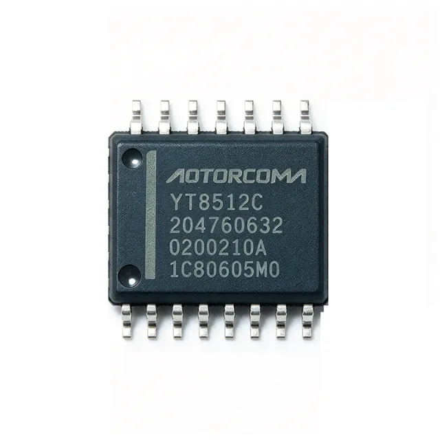
MAX195BCWE - 16-Bit 85ksps SAR ADC | Analog Devices | SOIC-16
The Analog Devices MAX195BCWE is a 16-bit, 85 ksps successive-approximation analog-to-digital converter (SAR ADC) with 10 µA shutdown mode, packaged in a 16-pin SO (SOIC-16, 0.3 inch wide) and capable of ±5V bipolar input ranges when used with an external reference. Per the Analog Devices product page, the MAX195 family is offered in 1ku list price tiers starting from $58.95, with the BCWE grade delivering B-grade linearity in a wide-body surface-mount footprint. An ADC (analog-to-digital converter) is a mixed-signal integrated circuit that quantizes a continuous analog input voltage into a discrete digital code. Successive-approximation (SAR) ADCs use an internal binary search against a reference to convert each sample in N clock cycles, trading off sample rate for resolution. The MAX195BCWE sits inside the broader hierarchy: SAR ADC -> ADC -> data converter -> mixed-signal IC -> semiconductor. SAR ADCs are favored over delta-sigma for multiplexed multi-channel data acquisition where low latency and deterministic throughput matter. Key features include 16-bit no-missing-code resolution, 85 ksps maximum sample rate, ±0.5 LSB (B-grade) integral nonlinearity, single +5V analog supply operation, and an SPI/QSPI/MICROWIRE-compatible serial interface. The MAX195 also provides unipolar (0V to VREF) or bipolar (-VREF to +VREF) input ranges selected by a single pin, and a hardware-shutdown mode that drops supply current to 10 µA for battery-powered portable instrumentation. Technically, the MAX195 uses an on-chip capacitive charge-redistribution DAC and an internal calibration cycle that corrects linearity and offset errors at power-up. Separate analog (AVDD) and digital (DVDD) supplies minimize digital-noise coupling into the analog input path, a critical detail for low-noise 16-bit signal chains. The part accepts an external reference up to +5V, allowing trade-offs between input range and thermal noise. Typical applications include industrial process control loops, portable data loggers, instrumentation front ends, weigh scales, and multi-channel data acquisition systems. The MAX195 is also widely used in legacy designs that require a 16-bit SAR ADC in a SOIC-16 footprint with SPI compatibility, where replacement parts must remain pin-compatible to avoid board rework. A practical design consideration: the external reference IC directly determines the converter's absolute accuracy and noise floor. Use a low-noise, low-drift reference such as the AD588 or MAX6350 for best 16-bit performance. Decouple AVDD and DVDD with separate 0.1 µF ceramic + 10 µF tantalum pairs to prevent digital switching noise from coupling into the analog front end. This page synthesizes distributor pricing, drop-in alternatives, and practical design notes not found in the bare manufacturer datasheet, including a cross-reference to SOIC-16 same-package parts verified on DigiKey, Mouser, and Octopart.