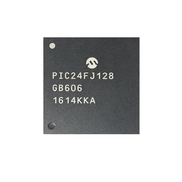
製品 (32840)

PIC24FJ128GB202T-I/SO - 16-bit MCU, 128KB Flash, USB-OTG, Crypto | Microchip
PIC24FJ128GB202T-I/SO

PIC24FJ128GB202T-I/SO - 16-bit MCU, 128KB Flash, USB-OTG, Crypto | Microchip

The Microchip Technology PIC24FJ128GB202T-I/SO is a 16-bit microcontroller built on the PIC24F eXtreme Low Power (XLP) architecture, delivering 16 MIPS performance at 32 MHz with 128 KB of Flash and 8 KB of SRAM, housed in a 28-pin SOIC (7.50 mm body) package. The device integrates a full-speed USB On-The-Go (OTG) transceiver, a hardware crypto engine with key storage, and a true random number generator, making it one of the most security-aware PIC24F devices on the market. A 16-bit microcontroller (MCU) is a programmable processor that executes instructions on 16-bit-wide data paths, sitting between 8-bit MCUs (lower cost, lower performance) and 32-bit MCUs (highest performance, higher cost) in the embedded hierarchy. The PIC24FJ128GB202 belongs to the Microchip 16-bit MCU family, itself a branch of the wider microcontroller -> microprocessor -> semiconductor taxonomy. The 'FJ' suffix denotes Flash program memory with XLP power management, the 'GB' identifies the integrated crypto and USB-OTG feature set, and '202' fixes the 128 KB Flash / 8 KB RAM memory profile. Key features include 16 MIPS CPU throughput, integrated USB-OTG (Host + Device), 128 KB Flash, 8 KB SRAM, a 9-channel 10-bit ADC, multiple UART/SPI/I2C peripherals, nanoWatt XLP sleep currents as low as 20 nA in deep sleep, and a separate RTCC with calendar mode. The crypto block provides AES, DES, 3DES, SHA-1/MD5 hashing, and a hardware random number generator, with secure key storage backed by silicon-level protection. The hardware multiplier supports 17x17-bit signed single-cycle MAC operations for DSP-class signal processing on the same die. Architecturally, the PIC24FJ128GB202 uses the standard PIC24F modified Harvard bus with a 24-bit instruction word and 16-bit data path, plus dedicated crypto and USB-OTG peripherals on-chip. The wide 3.3V core operates across 2.0-3.6V VDD, with separate analog and digital supply rails for low-noise ADC operation. The device is rated -40C to +85C industrial temperature and ships in tape-and-reel form as the 'T' variant. Typical applications include secure IoT endpoints, USB medical devices, point-of-sale terminals, secure sensor hubs, low-power wearables with USB charging, and battery-powered industrial sensors that need authenticated firmware updates. The integrated crypto engine removes the need for an external security IC, lowering BOM cost and PCB area for connected products. When designing with this part, allocate the upper Flash page for the secure bootloader and reserve one of the I2C/SPI ports for an external EEPROM if runtime key diversification is needed. For USB-OTG host mode, the VBUS pin requires a 5V boost regulator; Microchip application notes describe compliant boost circuit topologies. Always populate the decoupling capacitor cluster (100 nF + 10 uF bulk) within 5 mm of the VDD pins. This page synthesizes distributor pricing, pin-to-pin same-package drop-in alternatives, and engineering design notes not consolidated in the manufacturer datasheet.

見積もり お問い合わせ
PIC24FJ128GB202T-I/SS - 16-bit 32MHz USB MCU w/ Crypto | Microchip
PIC24FJ128GB202T-I/SS

PIC24FJ128GB202T-I/SS - 16-bit 32MHz USB MCU w/ Crypto | Microchip

The Microchip PIC24FJ128GB202T-I/SS is a 16-bit PIC24F microcontroller from the XLP™ 24F family, integrating a hardware crypto engine, key storage, and random number generator with 128 KB Flash and 8 KB RAM in a 28-pin SSOP package. It runs at up to 32 MHz (16 MIPS) and provides a USB 2.0 On-The-Go peripheral alongside a 10/12-bit ADC, making it a low-power mixed-signal MCU for secure connected embedded designs. What is a 16-bit microcontroller? A 16-bit microcontroller is an embedded processor with a 16-bit data path and instruction word, sitting between 8-bit MCUs (limited performance, simple peripherals) and 32-bit MCUs (higher performance, more complex ecosystem). The PIC24F family is Microchip's 16-bit entry, falling under the broader PIC microcontroller hierarchy: PIC24F -> 16-bit MCU -> microcontroller -> embedded processor -> semiconductor. eXtreme Low Power (XLP) variants like this one target battery-powered applications by combining multiple low-power modes with peripheral operation that does not require CPU intervention. Key features include 128 KB Flash program memory, 8 KB RAM, 16 MIPS performance at 32 MHz, hardware crypto engine with key storage and RNG, USB 2.0 full-speed On-The-Go with integrated PHY, a 10-bit ADC (1.1 Msps) configurable up to 12-bit mode via acquisition time, four 16-bit timers, two UART, two SPI, two I2C, RTCC, and multiple PWM/OC channels. The device operates from 2.0 V to 3.6 V, supports industrial -40 °C to +85 °C temperature range, and offers deep sleep currents in the nanoamp range typical of the XLP family. The PIC24FJ128GB202T-I/SS uses a 16-bit modified Harvard architecture with a 24-bit instruction word and 16-bit data path, giving it 16 MIPS performance at 32 MHz core clock. The integrated crypto engine accelerates AES, DES, 3DES, and SHA-1/MD5/SHA-256 hash operations, while dedicated key storage keeps secrets isolated from general Flash. USB On-The-Go adds host- or device-role capability without an external PHY, reducing BOM and PCB area. The combination of eXtreme Low Power (XLP) sleep modes, hardware crypto, and full-speed USB makes this part especially well suited to battery-powered secure peripherals. Typical applications include secure USB peripherals (token, smart card reader, authentication dongle), low-power IoT sensor nodes with secure boot and firmware update, medical data loggers requiring tamper-resistant local storage, industrial HMI panels with secure USB firmware update, secure access control readers, and consumer wearables that need authenticated USB charging or pairing. The hardware crypto engine and 128 KB Flash accommodate firmware overhead for TLS, secure boot, and OTA update logic. When designing with this device, allocate a dedicated 0.1 µF decoupling capacitor per power pin and place it within 5 mm of the IC. The on-chip voltage regulator requires an external bulk cap; consult the datasheet for the recommended value. Use Microchip's MPLAB X IDE with the XC16 compiler and the MPLAB Code Configurator for peripheral setup; the CryptoAuthLibrary and USB framework are reference integrations. The 'T' suffix denotes tape-and-reel packaging for high-volume assembly. This page synthesizes distributor pricing, drop-in same-package alternatives, comparison data, and practical design notes not found in the manufacturer datasheet alone, helping engineers evaluate the PIC24FJ128GB202T-I/SS for secure low-power USB designs.

見積もり お問い合わせ
PIC24FJ128GB204-E/PT - 16-bit 128KB Flash MCU w/ USB OTG | Microchip
PIC24FJ128GB204-E/PT

PIC24FJ128GB204-E/PT - 16-bit 128KB Flash MCU w/ USB OTG | Microchip

The Microchip Technology PIC24FJ128GB204-E/PT is a 16-bit PIC® XLP™ 24F microcontroller with 128KB Flash, 8KB RAM, an integrated USB 2.0 On-The-Go transceiver, and a hardware crypto engine, housed in a 44-pin TQFP (10x10 mm) package. It executes instructions at up to 32 MHz from a 2.0-3.6V supply and is specified for the extended -40°C to +125°C operating range. The combination of XLP (eXtreme Low Power) sleep currents in the sub-microamp range and on-chip peripheral DMA makes it suited to battery-powered secure peripherals and USB HID/CDC devices. What is a PIC24FJ microcontroller? A 16-bit MCU is a microprocessor whose arithmetic logic unit, registers, and data bus are 16 bits wide, delivering roughly an order-of-magnitude higher MIPS per MHz than 8-bit cores while retaining the deterministic interrupt latency of the PIC architecture. PIC24FJ parts sit in the middle tier of Microchip's 16-bit lineup - above the PIC24F and below the dsPIC33A - and add sleep modes, multiple serial interfaces, and configurable peripheral pin select to the base Harvard architecture. Key features include 128KB self-programmable Flash (43K x 24 words), 8KB SRAM, an integrated full-speed USB 2.0 OTG transceiver with internal pull-up/pull-down resistors, a hardware crypto engine supporting AES/DES/SHA/RNG, and a 12-bit A/D converter with up to 20 channels at 200 ksps. Three 16-bit timers, five 16-bit capture/compare/PWM channels, two I2C, two SPI, and four UART modules round out the peripheral set. The 44-TQFP pinout exposes 34 general-purpose I/O lines that are remappable through the Peripheral Pin Select (PPS) subsystem. Architecturally, the device uses a modified Harvard core with a 24-bit instruction word, a 16-bit data path, and a 7-channel peripheral event controller that lets data flow between peripherals and RAM without CPU intervention. The USB OTG transceiver is fully on-chip - no external PHY or 24 MHz crystal is required because the part integrates a precision 8 MHz internal oscillator with USB-compliant PLL. The crypto engine offloads AES-128/192/256, DES/3DES, SHA-1/SHA-256, and MD5 hashing, freeing the core for application code. Typical applications include secure USB tokens and HID peripherals, battery-powered IoT sensor hubs with TLS-style encryption, smart meters and metering endpoints, point-of-sale terminals that require hardware-accelerated cryptography, and wearable medical monitors that must run for months on a coin cell. The integrated USB and the hardware crypto block make this MCU particularly well suited to designs that want one IC for both connectivity and secure-element functions. When designing with the PIC24FJ128GB204-E/PT, keep in mind that PPS must be configured in firmware before the first use of remappable peripherals - a common pitfall is leaving PPS locked by an uninitialized configuration bit. A 10 µF plus 0.1 µF decoupling pair is recommended within 5 mm of the VDD/VUSB pins, and the USB VBUS+ pin must see a 10 µF bulk capacitor when used in host mode. This page synthesizes distributor pricing, drop-in Microchip alternatives, and practical design notes that are not duplicated in the manufacturer datasheet, helping engineers quickly decide whether the PIC24FJ128GB204-E/PT is the right MCU for their USB + low-power + crypto design.

見積もり お問い合わせ
PIC24FJ128GB204-I/ML - 16-bit XLP MCU 128KB Flash USB 44-QFN | Microchip
PIC24FJ128GB204-I/ML

PIC24FJ128GB204-I/ML - 16-bit XLP MCU 128KB Flash USB 44-QFN | Microchip

The Microchip Technology PIC24FJ128GB204-I/ML is a 16-bit PIC24F microcontroller with eXtreme Low Power (XLP) technology, integrating 128KB of Flash program memory, 8KB of RAM, a hardware crypto engine, and a full-speed USB 2.0 transceiver in a 44-pin QFN (8x8 mm) package. It runs up to 32 MHz, delivers 16 MIPS performance, and supports 1.8V to 3.6V operation, making it a drop-in fit for low-power secure embedded designs. According to the Microchip datasheet DS30005009C, the device is purpose-built for IoT nodes that need authenticated firmware, secure key storage, and battery-friendly standby draw. The PIC24F GB2 family is the entry point for Microchip's hardware cryptography roadmap, featuring an integrated AES engine, a true random number generator (RNG), and secure key storage. A PIC microcontroller (MCU) is a programmable embedded processor that integrates CPU core, non-volatile Flash memory, SRAM, and peripherals (timers, ADC, communication blocks) on a single die. The PIC24F family is Microchip's 16-bit segment sitting above the 8-bit PIC16/PIC18 lines, offering higher throughput, larger address space (24-bit instruction word), and richer peripherals such as USB, crypto accelerators, and capacitive touch sensing. The eXtreme Low Power (XLP) technology adds deep-sleep modes down to nanoamp-level standby current, expanding the hierarchy: PIC24FJ -> PIC24F family -> 16-bit MCU -> microcontroller -> embedded processor -> semiconductor. Key features of the PIC24FJ128GB204 include hardware AES-128 encryption, a true random number generator, secure key storage in OTP Flash, integrated USB 2.0 full-speed transceiver (host, device, OTG), up to 32 MHz operation (16 MIPS), 128KB Flash, 8KB SRAM, a 10-bit ADC with up to 200 ksps, multiple UART/SPI/I2C peripherals, and a real-time clock calendar (RTCC) with battery backup. The combination of crypto, USB, and XLP extends the application envelope beyond general-purpose microcontrollers into secure connected devices. Architecturally, the PIC24FJ128GB204 uses a modified Harvard architecture with a 16-bit data path and 24-bit instruction word, plus a peripheral bus that offloads DMA transfers. The hardware crypto engine runs AES-128 in hardware without CPU intervention, accelerating secure boot and TLS handshake operations. The integrated USB PHY eliminates external transceiver components, reducing BOM cost in HID, CDC, and mass-storage designs. Typical applications include IoT sensor nodes with secure firmware updates, USB peripherals (HID, CDC, mass storage), secure access control, smart energy metering, low-power wireless sensor hubs, medical telemetry, and consumer devices with secure boot requirements. The XLP nanoWatt technology supports multi-year battery life in sleep-dominated duty cycles. When designing, ensure that VDD decoupling follows the 100 nF + 1 uF + 10 uF rule per Microchip's recommended layout, and route the USB DP/DM pair as a 90-ohm differential with controlled impedance. The crypto module requires secure boot firmware flow to expose its full capability. This page consolidates distributor pricing, drop-in alternatives, and practical design notes beyond what is in the manufacturer datasheet alone.

見積もり お問い合わせ
PIC24FJ128GB204T-I/ML - 16-bit 32MHz 128KB Flash USB MCU
PIC24FJ128GB204T-I/ML

PIC24FJ128GB204T-I/ML - 16-bit 32MHz 128KB Flash USB MCU

The Microchip PIC24FJ128GB204T-I/ML is a 16-bit PIC24F microcontroller from the XLP (eXtreme Low Power) family, featuring an integrated cryptographic engine, key storage, hardware Random Number Generator (RNG), USB On-The-Go (OTG), and ISO 7816 smart-card interface. It runs at up to 32 MHz, integrates 128 KB of Flash program memory (43K x 24 words) and 8 KB of SRAM, and is housed in a 44-pin QFN (8x8 mm) surface-mount package with tape-and-reel packaging. The "T" suffix denotes tape-and-reel delivery, while "-I" indicates the -40C to +85C industrial temperature grade. A 16-bit PIC microcontroller is a modified-Harvard architecture MCU that executes 16-bit instructions in a single cycle, positioning it between 8-bit MCUs (PIC16/PIC18) and 32-bit Cortex-M parts. PIC24F belongs to the wider MCU -> microcontroller -> embedded controller -> semiconductor taxonomy and is targeted at applications that require more computational headroom and richer peripherals than 8-bit parts while preserving Microchip's MPLAB X toolchain and Harmony ecosystem familiarity. The cryptographic engine provides AES/DES/SHA hardware acceleration and secure key storage, making the GB2 family distinct from the GA2 family which lacks crypto. Key features include a 16-bit core with hardware multiply/divide, 12-bit ADC up to 500 ksps, multiple PWM/SCCP/MCCP timers, I2C/SPI/UART peripherals, RTCC, deep-sleep current down to a few hundred nA typical, and a full-speed USB 2.0 OTG controller with on-chip transceiver. The wide 2.0V-3.6V VDD range supports direct battery operation, and XLP technology extends battery life in duty-cycled applications. The crypto engine is selectable via user fuses, allowing OEMs to enable hardware AES only when needed to lower die exposure. The 44-QFN (8x8 mm) package exposes 35 I/O pins via Peripheral Pin Select (PPS), enabling flexible signal routing - a significant advantage over fixed-pin peripherals. Internal regulator, brown-out reset, and watchdog timer are integrated. The QFN exposed pad must be soldered for thermal performance and electrical ground return. Typical applications include secure IoT nodes, USB peripherals, smart-card readers, battery-powered sensors, medical instrumentation with secure data logging, industrial HMI panels, and access control terminals. Designers select the GB204 over the GA204 when cryptographic functions are required; the GA204 shares the same 44-QFN pinout but omits the crypto engine. When designing with this device, ensure the QFN exposed pad is soldered to a continuous ground plane with multiple thermal vias for heat dissipation. The PPS registers must be configured and unlocked before first peripheral use - lock-out after configuration prevents accidental runtime remapping. Decouple VDD with a 10 uF bulk plus 0.1 uF ceramic close to each VDD pin.

見積もり お問い合わせ
PIC24FJ128GB206-I/MR - 16-bit 32MHz 128KB Flash USB MCU | Microchip
PIC24FJ128GB206-I/MR

PIC24FJ128GB206-I/MR - 16-bit 32MHz 128KB Flash USB MCU | Microchip

The Microchip Technology PIC24FJ128GB206-I/MR is a 16-bit RISC microcontroller from the PIC24F "GB2" family featuring 128 KB of Flash, 96 KB of RAM, and integrated USB On-The-Go (OTG) with a random number generator and hardware crypto engine, housed in a 64-pin VQFN (9x9 mm) package with exposed thermal pad. It runs up to 32 MIPS from a 2.5 V / 3.3 V supply and belongs to the eXtreme Low Power (XLP) family, designed for secure, battery-friendly connected designs. What is a 16-bit microcontroller? A microcontroller (MCU) is a single-chip computer containing a CPU core, non-volatile program memory (Flash), volatile working memory (RAM), and a rich set of on-chip peripherals such as timers, communication interfaces, and analog blocks. The PIC24FJ128GB206-I/MR belongs to the broader taxonomy: microcontroller -> 16-bit MCU -> PIC24F family -> PIC24FJ GB2 sub-family -> Microchip 16-bit secure connectivity MCU. Key features include 128 KB (43K x 24) of self-programmable Flash, 96 KB of RAM, USB 2.0 OTG with dual-role (host or peripheral), integrated hardware crypto engine with key storage, a true random number generator, multiple UART/SPI/I2C peripherals, a 10-bit ADC, and a parallel master port for graphics displays. The XLP variant provides nanoWatt deep-sleep currents suitable for battery-powered applications. Architecturally, the device uses a modified Harvard RISC core with a 16-bit data path and 24-bit instruction width, supporting 32 MIPS at 32 MHz. Integrated peripherals are mapped via a Peripheral Pin Select (PPS) system, allowing flexible function-to-pin routing. The hardware crypto engine accelerates AES, DES, 3DES, SHA-1, SHA-256, and HMAC operations offloaded from the CPU. Typical applications include USB peripherals (HID, CDC, mass storage), secure IoT endpoints, battery-powered wearables, graphics display controllers, secure token/authentication devices, and industrial data loggers with on-board encryption. When designing, allocate adequate decoupling (100 nF + 4.7 µF) near each VDD pin and follow Microchip's PGEC/PGED layout guidelines. The parallel master port shares pins with several peripherals - planning the pin map early avoids late-stage rework. This page synthesizes distributor pricing, drop-in same-family alternatives, and design notes not consolidated on any single manufacturer or distributor page.

見積もり お問い合わせ
PIC24FJ128GB206T-I/MR - 16-bit 32MHz 128KB Flash MCU | Microchip
PIC24FJ128GB206T-I/MR

PIC24FJ128GB206T-I/MR - 16-bit 32MHz 128KB Flash MCU | Microchip

The Microchip Technology PIC24FJ128GB206T-I/MR is a 16-bit PIC microcontroller from the PIC24FJ GB2 family, integrating 128KB of Flash program memory and 96KB of RAM, running at up to 32MHz (16 MIPS) at 3.3V, and housed in a 64-pin VQFN (9x9) package with an exposed thermal pad. It is supplied on tape-and-reel (T/R) with an industrial -40C to +85C temperature range. What is a PIC24F microcontroller? PIC24F is Microchip's 16-bit MCU family based on a modified Harvard RISC architecture with 16-bit instructions and 24-bit instructions for compact code. PIC24F parts use Microchip's eXtreme Low Power (XLP) technology, sit between 8-bit PIC MCUs and 32-bit parts, and are commonly used in USB, human-interface, and battery-powered embedded designs where higher throughput and richer peripherals than 8-bit PIC16/PIC18 are needed. Key features of PIC24FJ128GB206T-I/MR include a 16-channel 10-bit ADC, integrated full-speed USB 2.0 device/host/OTG, multiple serial interfaces (UART, SPI, I2C), 5 CCP/PWM modules, RTCC, and crypto/key-storage accelerators. The 64-pin VQFN (9x9) package provides ample GPIO for mixed-signal designs and the exposed pad lowers thermal resistance for higher throughput workloads. Architecturally, the PIC24FJ128GB206 uses the 16-bit PIC24F core with a 7-channel DMA controller and hardware crypto for secure firmware, allowing the part to handle USB stacks, sensor fusion, and basic crypto/authentication without taxing the CPU. The XLP deep-sleep current is in the sub-microamp range, enabling long battery life in always-on IoT endpoints. Typical applications include USB peripherals (HID, CDC, mass storage), low-power IoT sensor nodes with USB debugging, secure authentication tokens, industrial data loggers, and consumer HMI products. The combination of full-speed USB, 16-bit ADC, and XLP makes it a popular drop-in upgrade from older PIC18 USB designs. When designing with this device, ensure the VQFN-9x9 exposed pad is soldered to a sufficiently large copper pour to meet thermal and electrical grounding requirements. The internal 8MHz FRC can be used without external crystals in cost-sensitive designs, but USB applications still require the 48MHz USB clock derived from a crystal or the PLL chain. This page synthesizes distributor pricing, same-brand drop-in alternatives (including tape-and-reel and tray variants), and practical design notes not found in the manufacturer datasheet alone.

見積もり お問い合わせ
PIC24FJ128GB210-I/BG - 16-bit 32MHz 128KB Flash USB MCU | Microchip
PIC24FJ128GB210-I/BG

PIC24FJ128GB210-I/BG - 16-bit 32MHz 128KB Flash USB MCU | Microchip

The Microchip Technology PIC24FJ128GB210-I/BG is a 16-bit Flash microcontroller from the PIC24F family with integrated USB On-The-Go (OTG) support, offering 128KB of Flash program memory, 96KB of RAM, and a maximum CPU speed of 32MHz (16 MIPS) in a 121-pin TFBGA (10x10 mm) package. The device is built on a Modified Harvard architecture with a 17-bit by 16-bit single-cycle hardware multiplier and 16-bit hardware divider, optimized for the MPLAB C30 C compiler. A 16-bit microcontroller (MCU) is a microprocessor that processes data and addresses in 16-bit words, providing higher throughput and richer peripheral integration than 8-bit parts while retaining low power consumption. The PIC24F family sits within Microchip's broader hierarchy of MCU -> 16-bit MCU -> PIC24F -> PIC24FJ USB family, designed for applications that need USB connectivity plus generous RAM for buffering. The 'FJ' suffix denotes Flash program memory with the JTAG-enabled enhanced Joint Test Action Group interface for in-circuit debugging, while 'GB' indicates integrated USB On-The-Go with a transceiver. Key features include USB 2.0 OTG with dual-role (Host or Device) capability, low-speed (1.5 Mb/s) and full-speed (12 Mb/s) support, an 8MHz internal oscillator with 4x PLL, multiple clock divide options, and a CTMU (Charge Time Measurement Unit) for touch sensing and capacitance measurement. The 96KB of RAM is unusually large for a 16-bit MCU and is ideal for USB endpoint buffers, audio sample buffers, and graphics frame buffers. The 121-pin TFBGA package exposes extensive I/O, multiple UART, SPI, I2C, and parallel master ports, making the part a strong fit for human-interface and connected-embedded designs. Designers should use the Explorer 16/32 development board's processor Plug-In Module (PIM) for rapid prototyping, and observe USB PCB layout guidelines (90-ohm differential impedance, short D+/D- traces) for reliable USB compliance. Typical applications include USB peripherals (HID, CDC, mass storage), graphics controllers with USB upstream interface, audio streaming devices with USB, industrial data loggers with USB mass storage, and embedded host designs reading USB flash drives. This page synthesizes distributor pricing, drop-in same-family alternatives, and practical design considerations not consolidated on a single manufacturer page.

見積もり お問い合わせ
PIC24FJ128GB406-I/MR - 16-bit MCU, 128KB Flash, USB OTG, 64-QFN | Microchip
PIC24FJ128GB406-I/MR

PIC24FJ128GB406-I/MR - 16-bit MCU, 128KB Flash, USB OTG, 64-QFN | Microchip

The Microchip Technology PIC24FJ128GB406-I/MR is a 16-bit PIC24F microcontroller operating at up to 32 MHz (16 MIPS) with 128 KB of Flash program memory (43 K x 24 words) and 16 KB of RAM, housed in a 64-pin QFN (9 x 9 mm) package with an exposed thermal pad. What is a PIC24F microcontroller? The PIC24F is a 16-bit modified-Harvard MCU family from Microchip positioned between 8-bit PIC16/PIC18 parts and 32-bit PIC32 parts. Within the PIC taxonomy it sits in the middle tier, delivering higher performance than 8-bit parts while retaining low-power XLP modes. It belongs to the broader class of microcontrollers (MCUs) inside embedded processors, which are themselves a category of integrated circuits used for digital control. The PIC24FJ128GB406 adds a hardware cryptography engine, full-speed USB On-The-Go (OTG), an LCD segment driver, and extreme low-power (XLP) sleep currents below 1 uA in deep sleep. Key features include the integrated AES/Hardware Crypto peripheral (suitable for 128/192/256-bit AES in hardware), a 16-channel 10-bit A/D converter with 500 ksps throughput, four UART modules, three SPI, three I2C, a Parallel Master Port, and a Peripheral Pin Select (PPS) system that remaps digital peripherals to any I/O. The wide 2.0 V to 3.6 V supply range allows direct Li-Ion battery operation, and the 16 MIPS core plus DMA controller keep the CPU off-load for USB isochronous traffic. The architecture pairs a 16-bit ALU with a C compiler-friendly instruction set, deterministic interrupt latency, and a small 31-element instruction shadow set for real-time tasks. The 128 KB Flash supports self-programming, and the ICSP/In-Circuit Serial Programming header lets the part be programmed on the board. Typical applications include USB HID/CDC peripherals, secure IoT sensor nodes, electronic access control with LCD keypads, low-cost AES-secured data loggers, and battery-powered industrial HMIs. The combination of integrated crypto, USB OTG, and LCD driver removes the need for an external crypto companion chip in many designs. When designing with this part, ensure the Vbus/Vbuson and D+/D- traces are length-matched within 150 mils and routed to a USB-compliant 90-ohm differential impedance. Place a 1 uF X7R bypass within 3 mm of every VDDA/Vcap pin and connect the exposed pad to a continuous ground plane for thermal dissipation. This page synthesizes live distributor pricing, drop-in same-package alternatives, and practical design notes drawn from the manufacturer datasheet and reference designs - information not collated on a single distributor product page.

見積もり お問い合わせ
PIC24FJ128GB410-I/PT - 16-bit 32MHz MCU, 128KB Flash, USB-OTG | Microchip
PIC24FJ128GB410-I/PT

PIC24FJ128GB410-I/PT - 16-bit 32MHz MCU, 128KB Flash, USB-OTG | Microchip

The Microchip Technology PIC24FJ128GB410-I/PT is a 16-bit PIC24F microcontroller featuring 128 KB Flash, 16 KB RAM, integrated Hardware Crypto module, full-speed USB-OTG, segmented LCD driver, and Microchip's eXtreme Low Power (XLP) technology, all housed in a 100-pin TQFP (12x12 mm) package. It executes instructions at 16 MIPS from a 32 MHz internal oscillator, with hardware cryptographic acceleration supporting AES, DES, 3DES, SHA-1, SHA-256, MD5, and HMAC. A microcontroller (MCU) is a single-chip computer that integrates a CPU core, program memory, data RAM, and peripherals. The PIC24F family sits in Microchip's 16-bit MCU portfolio between 8-bit PIC18 and 32-bit PIC32MX/dsPIC devices, optimized for ultra-low-power and mixed-signal applications. Microcontrollers belong to the broader category of embedded processors and are the building blocks of nearly every electronic product, from battery-powered IoT nodes to industrial HMI panels. Key features include 128 KB self-programmable Flash (43K x 24 instruction words), 16 KB SRAM, 4 KB auxiliary Flash for EEPROM emulation, hardware crypto engine, USB-OTG with PHY, segment LCD driver up to 128 segments, 4 UARTS, 4 SPI, 5 I2C, 16-bit timers, 12-bit A/D up to 1 Msps, and CTMU for capacitive measurement. The XLP technology enables nanoWatt deep-sleep currents as low as 20 nA in Sleep mode and 1.8 µA in RTCC mode, making it suitable for battery-powered designs. The 16-bit modified-Harvard architecture with separate program and data buses enables deterministic interrupt latency and single-cycle 16-bit multiply, while the peripheral pin select (PPS) remapping subsystem simplifies PCB routing. The hardware crypto engine performs AES in 1.6 µs/MB and SHA-256 in 2.6 µs/block, offloading the CPU and reducing firmware complexity. Typical applications include secure IoT sensor nodes, USB medical devices, secure access control, smart metering with LCD, industrial HMI, and battery-powered data loggers. The integrated USB-OTG PHY enables it to act as either USB host or device without external components. Design consideration: route VDD/VSS pairs to each pin pair, place a 100 nF decoupling capacitor within 3 mm of every VDD pin, and connect the on-board 32 kHz secondary oscillator pins to a watch crystal for accurate RTCC. The Hardware Crypto module requires firmware initialization before use. This page synthesizes distributor pricing, drop-in same-package alternatives, and practical design notes that go beyond what the manufacturer datasheet alone provides.

見積もり お問い合わせ
PIC24FJ128GB412T-I/BG - 16-Bit 32MHz 128KB Flash MCU | Microchip
PIC24FJ128GB412T-I/BG

PIC24FJ128GB412T-I/BG - 16-Bit 32MHz 128KB Flash MCU | Microchip

The Microchip Technology PIC24FJ128GB412T-I/BG is a 16-bit PIC24F microcontroller featuring eXtreme Low Power (XLP) technology, integrated hardware cryptographic acceleration, USB OTG, and an LCD driver. The device delivers 32 MHz (16 MIPS) performance from 128 KB dual-partition Flash and 16 KB SRAM, all housed in a 121-ball TFBGA package measuring 10x10 mm with industrial -40 to +85 C temperature range. An MCU (microcontroller) is a single-chip computer that integrates a CPU core, program memory (Flash), data memory (SRAM), and a rich set of peripherals into one IC. The PIC24F family targets low-power embedded applications; PIC24FJ128GB412 specifically belongs to the GB412 sub-family distinguished by its hardware crypto engine (AES/SHA/RNG), USB 2.0 On-The-Go controller with integrated PHY, segment-LCD driver, and 128 KB Flash with dual-partition safety features for fail-safe firmware updates. Key features include an integrated hardware cryptographic module supporting AES, DES, 3DES, SHA-1, SHA-256 and true random number generation; 16 channels of 10-bit ADC; four UART, three SPI, three I2C, and a parallel port; CTMU for capacitive touch sensing; and eXtreme Low Power modes drawing under 1 uA in deep sleep. The device operates from 2.0V to 3.6V and includes a peripheral pin select (PPS) system that allows flexible remapping of digital peripherals to physical pins. The PIC24FJ128GB412 uses a Harvard-architecture 16-bit CPU with modified RISC instruction set supporting atomic bit operations, 16x16 hardware multiply in a single cycle, and DSP-friendly instructions. The dual-partition Flash allows live firmware updates without bricking the device - critical for IoT and medical devices requiring field updates. Typical applications include secure IoT endpoints with TLS/DTLS firmware, USB peripherals such as barcode scanners and POS terminals, segment-LCD human-machine interfaces (HMIs), battery-powered medical devices needing eXtreme Low Power sleep, secure token authenticators, industrial sensor nodes, and USB-C chargers with authentication. The hardware crypto engine accelerates TLS handshakes and secure boot. When designing with this device, allocate careful attention to USB OTG routing, place the 121-ball TFBGA decoupling capacitors immediately under the package, and review the dual-partition bootloader flow for fail-safe OTA updates. JTAG/ICSP programming pins (PGECx/PGEDx) require a dedicated pair - all VDD/VSS balls must be connected for correct operation. This page synthesizes distributor pricing, verified drop-in alternatives, and engineering design notes not found in the standalone Microchip datasheet, giving buyers and design engineers a complete decision-ready view of the PIC24FJ128GB412T-I/BG.

見積もり お問い合わせ
PIC24FJ128GB606-E/MR - 16-Bit 32MHz 128KB Flash USB MCU | Microchip
PIC24FJ128GB606-E/MR

PIC24FJ128GB606-E/MR - 16-Bit 32MHz 128KB Flash USB MCU | Microchip

The Microchip Technology PIC24FJ128GB606-E/MR is a 16-bit RISC PIC microcontroller with 128KB Flash, 32KB RAM, and integrated USB On-The-Go (OTG) full-speed support, housed in a 64-pin VQFN (9x9 mm) package with exposed thermal pad. It operates from a 2.0V to 3.6V supply, runs at up to 32MHz CPU clock, and belongs to the PIC24F family of low-power XLP microcontrollers. The IC ships in tube packaging and is qualified to AEC-Q100 for automotive applications. A microcontroller (MCU) is a single-chip computer that integrates a CPU core, program memory (Flash), data memory (RAM), peripherals, and I/O into one package. Within the broader semiconductor taxonomy, an MCU belongs to: microcontroller -> embedded processor -> digital IC -> integrated circuit. The PIC24F family uses a 16-bit modified-Harvard architecture with a 24-bit instruction word, providing higher code density than 8-bit MCUs while remaining cost-competitive for embedded designs. Key features include 128KB (43K x 24) dual-partition Flash with Live Update capability for field-firmware upgrades without downtime, 32KB RAM, integrated USB 2.0 full-speed OTG with PHY, and the eXtreme Low Power (XLP) technology that delivers nanoWatt standby currents below 20 nA in deep sleep. The device provides multiple communication peripherals (UART, SPI, I2C), a 16-channel 10/12-bit ADC, five 16-bit timers, and up to 53 I/O pins. The architecture supports Peripheral Pin Select (PPS) remappable I/O, allowing flexible PCB routing. The dual-partition Flash with Live Update is engineered for applications that cannot tolerate firmware-update downtime, such as industrial controllers, medical devices, and USB-connected peripherals. Hardware CRC, a real-time clock calendar (RTCC), and a 32kHz secondary oscillator support battery-backed operation. Typical applications include USB peripherals (Human Interface Devices, mass storage, CDC serial bridges), industrial sensor hubs, automotive body and infotainment subsystems, portable medical/fitness devices, low-power IoT edge nodes, and consumer electronics with USB connectivity and firmware-update requirements. When designing with this MCU, choose decoupling per Microchip's application note AN584 (typically 100 nF + 10 uF near each supply pin), and ensure the exposed thermal pad is soldered to a sufficient copper pour to meet the package thermal resistance. The Live Update feature requires dual-image flash partitioning in linker configuration. This page synthesizes distributor pricing, drop-in compatible alternatives from the PIC24FJ family, and practical design notes not consolidated in the manufacturer datasheet.

見積もり お問い合わせ
PIC24FJ128GB606-I/MR - 16-bit 32MHz 128KB Flash USB MCU | Microchip
PIC24FJ128GB606-I/MR

PIC24FJ128GB606-I/MR - 16-bit 32MHz 128KB Flash USB MCU | Microchip

The Microchip Technology PIC24FJ128GB606-I/MR is a 16-bit PIC24F microcontroller running up to 32 MHz (16 MIPS), integrating 128 KB dual Flash program memory plus 32 KB RAM, full-speed USB On-The-Go (OTG), and a 53-I/O footprint, all housed in a 64-pin 9x9 mm QFN package. Targeted at low-power USB-embedded designs, it carries on-chip peripherals including 10/12-bit ADC, charge-time measurement unit (CTMU), configurable logic cells (CLC), and live-update Flash partitioning for safe firmware field upgrades. A microcontroller (MCU) is an integrated circuit that combines a CPU core, program memory (Flash), working memory (RAM), and a configurable set of peripherals such as timers, ADC, communication controllers, and I/O pins, all on a single die. Within the broader semiconductor taxonomy, a PIC24F MCU belongs to the family of 16-bit microcontrollers, which sit above 8-bit MCUs in compute and memory capability but below 32-bit Cortex-M and high-end application processors. PIC24F parts in particular target low-power, USB- or graphics-friendly embedded designs, balancing deterministic 16-MIPS throughput with eXtreme Low Power (XLP) sleep modes. Key differentiating features of the PIC24FJ128GB606 include dual-bank Flash with Live Update (enabling firmware swap without device reset), 128 KB program Flash (43K x 24 words), 32 KB RAM, full-speed USB 2.0 OTG with on-chip transceiver, 53 general-purpose I/O, peripheral-pinning remapping, multiple serial interfaces (UART, SPI, I2C), a real-time clock calendar (RTCC) with on-chip 32 kHz oscillator, and XLP technology for sub-uA sleep current. Architecturally, the PIC24FJ128GB606 uses Microchip's 16-bit modified-Harvard core with a 24-bit instruction word, delivering up to 16 MIPS at 32 MHz while operating from a single 2.0 V to 3.6 V supply. The dual-panel Flash memory plus a small boot Flash row supports field firmware updates via Live Update: code can be written to the inactive panel while the active panel continues to run, then a controlled swap is performed - useful for industrial and IoT devices that cannot tolerate shutdown during firmware upgrades. On-chip peripherals are mapped through Peripheral Pin Select (PPS), giving the designer flexibility to assign digital peripherals to a wide range of I/O pins without hardware rework. Typical applications include USB peripherals (HID, CDC, mass storage, audio class), industrial sensor hubs, portable data loggers, USB-connected human-interface devices, and low-power wireless sensor nodes bridging to external radios. The integrated CTMU makes the device a strong fit for capacitive-touch keypads, time-of-flight measurements, and precision analog front ends using the on-chip 10/12-bit ADC. The 53-I/O count also suits mixed-signal control boards that previously required a 64/80/100-pin PIC24, enabling footprint reduction when migrating a panel to a smaller 64-pin QFN. Designers should note that the MR suffix indicates a QFN-64 (9x9 mm) package with an exposed thermal pad (EP); the exposed pad must be soldered to a properly sized copper island on the PCB for thermal relief and electrical ground. Power decoupling should follow Microchip's typical-application guidance: 0.1 uF and 1 uF ceramic caps placed within 5 mm of the VDD/VSS pairs, plus a 4.7 uF bulk cap on the main rail. For USB OTG operation, the internal 3.3 V regulator must be enabled and a 1 uF cap placed on the VUSB3V pin per the manufacturer datasheet. This page synthesizes distributor pricing, drop-in alternatives from Microchip's own 24FJ product family and cross-brand references, and practical design notes not found in the bare datasheet, giving procurement and firmware teams a one-stop reference for the PIC24FJ128GB606-I/MR.

見積もり お問い合わせ
PIC24FJ128GB606-I/PT - 16-bit 32MHz 128KB Flash USB MCU | Microchip
PIC24FJ128GB606-I/PT

PIC24FJ128GB606-I/PT - 16-bit 32MHz 128KB Flash USB MCU | Microchip

The Microchip Technology PIC24FJ128GB606-I/PT is a 16-bit PIC24F microcontroller with a 32 MHz CPU core, 128 KB of dual-partition Flash with ECC, 32 KB of RAM, integrated USB On-The-Go (OTG) connectivity, and 53 general-purpose I/O lines, housed in a 64-pin TQFP (PT) package measuring 10x10 mm. The part is part of the eXtreme Low Power (XLP) family and supports Live Update firmware boot from two independent Flash partitions. A 16-bit MCU is a microcontroller whose CPU datapath, registers, and ALU operate on 16-bit-wide data words, giving roughly twice the throughput and code density of an 8-bit core while retaining deterministic real-time behaviour. The PIC24F family sits in the PIC24 -> 16-bit MCU -> microcontroller -> embedded processor hierarchy, combining moderate DSP-style performance with the broad peripheral integration (USB, PWM, ADC, comparators) typical of modern mixed-signal embedded controllers. The 'GB' suffix denotes the USB-OTG-enabled sub-family, and the '606' member is the 64-pin variant of the 64/80/100-pin PIC24FJ128GBx06 series. Key features include a hardware multiplier and divider, seven 16-bit timers, six PWM channels, a 12-bit A/D converter with multiple input channels, multiple UART/SPI/I2C interfaces, RTCC, and an integrated full-speed USB 2.0 OTG transceiver. The XLP architecture delivers deep sleep currents in the nanoamp range while maintaining RAM retention, and the dual-partition Flash with ECC enables robust Live Update firmware without bricking risk. Typical applications include USB human-interface devices (HID), consumer audio accessories, USB-to-UART bridges, industrial sensor hubs with USB diagnostics, low-power battery-powered data loggers, and embedded control boards that need firmware field-update capability. Designers often pair the part with external serial EEPROM for data logging and a USB type-A or micro-B connector for host/device toggling. When designing with this MCU, ensure the USB D+/D- traces are 90-ohm differential and length-matched, place the decoupling network as close to the VDD/VSS pins as possible, and configure the VUSB3V3 pin with the recommended 4.7 uF + 0.1 uF capacitor stack. The dual-partition Live Update feature requires the application firmware to implement the bootloader protocol documented in the family reference manual. This page synthesises distributor pricing, drop-in package-equivalent parts, and practical design notes not found in the manufacturer datasheet.

見積もり お問い合わせ
PIC24FJ128GB606T-I/MR - 16-bit 32MHz USB MCU, 128KB Flash, 64-QFN
PIC24FJ128GB606T-I/MR

PIC24FJ128GB606T-I/MR - 16-bit 32MHz USB MCU, 128KB Flash, 64-QFN

The Microchip Technology PIC24FJ128GB606T-I/MR is a 16-bit PIC24F microcontroller running up to 32MHz (16 MIPS) with 128KB of dual-partition flash (43K x 24 words) and 32KB SRAM, housed in a 64-pin QFN (9x9 mm) package with exposed pad. It integrates a USB-OTG (On-The-Go) transceiver, a CTMU (Charge Time Measurement Unit), multiple Configurable Logic Cells (CLC), three on-chip analog comparators, eight DMA channels, six PWM channels, and seven timer/counters in a single CMOS die optimized for low-power embedded USB designs. A 16-bit microcontroller is a class of embedded processor whose arithmetic logic unit, registers, and data paths are 16 bits wide, sitting between 8-bit MCUs (e.g. classic PIC16/PIC18, ATmega) and 32-bit Cortex-M parts. PIC24F devices use a modified Harvard architecture with separate program and data buses, peripheral pin-select remapping, and Microchip's nanoWatt XLP technology for sleep currents measured in nanoamps. The PIC24FJ128GB606 family adds a USB-OTG full-speed transceiver and dual-partition flash with Live Update for field-deployable firmware upgrades without device downtime. The dual-partition flash layout lets the firmware bootloader swap between two independently erasable image banks, a critical feature for devices that cannot be powered down during updates. CLC blocks allow logic glue (AND/OR/XOR/D-Flip-Flop) to be synthesized in silicon without external gates, while the CTMU enables touch, proximity, and time-of-flight measurements by sourcing a constant current through a sensor pad. The integrated USB-OTG controller eliminates an external PHY for HID, CDC, vendor-class, and battery-charger (BC1.2) applications. Typical applications include USB HID peripherals, USB-to-UART bridges, capacitive-touch user interfaces, low-power IoT sensor nodes, and industrial control panels. Industrial- and consumer-grade silicon grading (I-suffix) targets an ambient operating window of -40C to +85C. With 128KB flash and 32KB RAM, the device balances code density for USB stacks with adequate headroom for application buffers. Design considerations include the mandatory exposed pad solder connection for thermal dissipation and ground reference, plus careful USB DP/DM trace routing to maintain 90ohm differential impedance. The wide VDD range of 2.0V-3.6V supports direct Li-ion and 3.3V regulated supplies, while internal LDO regulation for the core simplifies multi-rail designs. This page synthesizes distributor pricing, drop-in alternatives from the same PIC24FJ family, and practical design notes not found in the manufacturer datasheet.

見積もり お問い合わせ
PIC24FJ128GB610T-I/BG - 16-bit 32MHz 128KB Flash MCU | Microchip
PIC24FJ128GB610T-I/BG

PIC24FJ128GB610T-I/BG - 16-bit 32MHz 128KB Flash MCU | Microchip

The Microchip PIC24FJ128GB610T-I/BG is a 16-bit microcontroller IC from the PIC24F family running at 32 MHz with 128 KB of dual Flash program memory (43K x 24) and 32 KB of RAM, housed in a 121-pin TFBGA package measuring 10x10 mm. It is part of the XLP (eXtreme Low Power) family and integrates a USB-OTG controller, making it suitable for connected embedded designs. The 121-TFBGA package (BG suffix) provides a compact footprint with a 0.8 mm ball pitch for high-density PCB layouts. A 16-bit microcontroller (MCU) is a microcontroller whose central processing unit operates on 16-bit data words and addresses, placing it above typical 8-bit MCUs (such as the PIC16 or AVR families) but below 32-bit Cortex-M parts in both arithmetic throughput and toolchain complexity. The PIC24F series in particular targets low-power applications with on-chip peripherals like USB, ADCs, and charge-time measurement units (CTMU), positioning it between simple 8-bit controllers and full 32-bit application processors. The 'F' suffix denotes Flash program memory with on-chip reprogrammability, supporting Microchip's Live Update dual-image boot mechanism. Key features of the PIC24FJ128GB610T-I/BG include 16 MIPS CPU performance at 32 MHz, integrated USB-OTG with on-chip transceiver, 85 digital I/O pins, dual-bank Flash supporting field firmware updates without downtime, multiple 12-bit and 10-bit ADC configurations (up to 24 channels of 12-bit ADC), and the XLP ultra-low-power modes that deliver nanoWatt sleep currents suitable for battery-powered IoT nodes. The CTMU peripheral supports capacitive touch sensing, while the CLC (Configurable Logic Cell) and PPS (Peripheral Pin Select) blocks enable flexible signal routing. The architecture combines a 16-bit modified Harvard CPU with a C-optimized instruction set, supporting peripheral operation through dedicated DMA channels and interrupt priority levels. The on-chip dual Flash design enables Live Update firmware upgrades - one bank runs application code while the other receives the new image, eliminating downtime in deployed products. Typical applications include USB peripherals (HID, CDC, mass storage), industrial sensing nodes, home automation gateways, low-power portable medical devices, automotive body electronics, and human-interface products with capacitive touch buttons. The 121-TFBGA package is best suited for high-density boards where maximum I/O and small footprint matter more than easy hand-soldering. Designers should note that the TFBGA package requires reflow soldering and X-ray or AOI inspection, making it unsuitable for hand assembly or low-volume prototyping. Decoupling follows Microchip's recommended 0.1 uF + bulk capacitor topology near each VDD/VDDCORE pair, and unused pins should be configured as outputs low to minimize leakage. This page synthesizes distributor pricing from DigiKey, drop-in alternatives from Microchip's PIC24F family cross-reference, and practical design considerations for the 121-TFBGA footprint that are not consolidated in the manufacturer datasheet.

見積もり お問い合わせ
PIC24FJ128GC006T-I/MR - 16-bit 32MHz 128KB Flash MCU | Microchip
PIC24FJ128GC006T-I/MR

PIC24FJ128GC006T-I/MR - 16-bit 32MHz 128KB Flash MCU | Microchip

The Microchip Technology PIC24FJ128GC006T-I/MR is a 16-bit PIC® XLP™ 24F microcontroller delivering 32 MHz CPU performance with 128 KB (43K x 24) of embedded Flash program memory, housed in a 64-pin VQFN (MR) 9x9 mm package. It targets portable and industrial applications that require low-noise analog signal acquisition combined with deterministic 16 MIPS throughput at 3.3 V. Integrated Intelligent Analog peripherals and eXtreme Low Power (XLP) technology reduce bill-of-materials count while extending battery life in always-on systems. A microcontroller (MCU) is a single-chip computer that integrates a CPU core, volatile and non-volatile memory, and programmable peripherals such as analog-to-digital converters, timers, communication interfaces, and general-purpose I/O. The PIC24F family uses a 16-bit modified Harvard RISC architecture, occupying the hypernym chain MCU -> microcontroller -> embedded processor -> semiconductor. The '24F' series emphasizes low power consumption and rich analog integration, making it distinct from higher-performance '24H' and '24E' variants that target motor control and graphics applications. Key differentiating features include 128 KB Flash plus 8 KB SRAM, segmented LCD driver support, USB 2.0 full-speed connectivity, a 12-bit A/D converter with up to 16 channels, multiple timers, and Microchip's eXtreme Low Power nanoWatt XLP technology. The 'T' suffix designates Tape and Reel packaging, while the 'I' suffix indicates the industrial -40 °C to +85 °C operating temperature range. The 64-VQFN (MR) 9x9 mm package provides an exposed thermal pad enabling higher dissipation in space-constrained PCB layouts. Architecturally, the PIC24FJ128GC006 integrates a precision 16-bit instruction set with hardware multiplier and divider, dual I/O ports, and the Intelligent Analog subsystem that combines op-amps, comparators, and references in a single die. This integration reduces external component count and PCB area while improving noise immunity for sensor front-end designs. Typical applications include portable medical devices, industrial sensor hubs, USB-based data loggers, smart energy metering with LCD readout, and battery-powered IoT edge nodes. The combination of LCD driver and USB enables compact human-interface products. Designers should budget thermal dissipation for the 9x9 mm QFN pad area, follow Microchip's decoupling guidance with 100 nF + bulk capacitors near VDD pins, and use trace routing that respects the analog/digital partition documented in the device datasheet.

見積もり お問い合わせ
PIC24FJ128GC006T-I/PT - 16-Bit 32MHz 128KB Flash MCU | Microchip
PIC24FJ128GC006T-I/PT

PIC24FJ128GC006T-I/PT - 16-Bit 32MHz 128KB Flash MCU | Microchip

The Microchip Technology PIC24FJ128GC006T-I/PT is a 16-bit PIC® XLP™ 24F microcontroller running at 32 MHz, delivering 128 KB of Flash program memory and 8 KB of SRAM, in a 64-pin TQFP (10x10 mm) package. It is part of the PIC24FJ128GC006 family of "Intelligent Analog" parts, integrating a 16-bit Sigma-Delta ADC, a 12-bit 10 MSPS pipeline ADC, dual 10-bit 1 MSPS DACs, and two on-chip operational amplifiers for precision signal conditioning. A microcontroller (MCU) is a single-chip computer that integrates a CPU core, program and data memory, peripherals, and I/O on one die. The PIC24F family uses a 16-bit modified Harvard architecture with a wide 24-bit instruction word, sitting above 8-bit PIC MCUs and below 32-bit ARM Cortex-M devices in performance, cost, and power hierarchy. The "XLP" (eXtreme Low Power) designation means this part targets battery-backed and energy-harvesting designs, complementing standard PIC24F parts. Key differentiating features include a USB On-The-Go (OTG) full-speed peripheral for direct device/host connectivity without an external bridge, a segmented LCD driver supporting glass up to several hundred segments, and the dual-ADC architecture that lets the same MCU digitize both high-bandwidth signals (12-bit pipeline at 10 MSPS across 30 channels) and high-resolution low-frequency signals (16-bit Sigma-Delta) for weigh-scale, temperature, or strain-gauge front ends. The 2x on-chip op-amps further reduce external analog count. Architecturally, the part leverages Microchip's standard PIC24F core with hardware multiplier, single-cycle MAC, and a 16-bit-wide datapath. Integrated Intelligent Analog reduces BOM by absorbing signal-chain functions that would otherwise need dedicated analog ICs, while 32 MHz operation gives ~16 MIPS throughput for signal processing and USB protocol stacks. Typical applications include portable medical instrumentation (glucose meters, pulse oximeters), industrial sensor transmitters, USB-connected data loggers, and battery-powered metering. The wide analog integration makes it especially suitable where board space, BOM cost, and low quiescent current matter more than raw CPU horsepower. When designing with this MCU, budget the I/O count against the 64-pin TQFP carefully - several pins are multiplexed with analog and LCD functions. Plan the PCB layout so the analog grounds are isolated from digital switching currents, especially with USB present. This page synthesizes distributor pricing, verified same-family drop-in alternatives, and practical design notes not found on the manufacturer datasheet, giving engineers a single decision-ready reference.

見積もり お問い合わせ
PIC24FJ128GC010T-I/BG - 16-bit 128KB Flash MCU w/ USB, LCD & XLP | Microchip
PIC24FJ128GC010T-I/BG

PIC24FJ128GC010T-I/BG - 16-bit 128KB Flash MCU w/ USB, LCD & XLP | Microchip

The Microchip Technology PIC24FJ128GC010T-I/BG is a 16-bit PIC24F microcontroller from the XLP™ (eXtreme Low Power) family, integrating 128 KB of Flash program memory (43K x 24 words) with a 32 MHz maximum operating frequency in a 121-pin TFBGA (10x10 mm) surface-mount package. Tape-and-reel (T/R) packaging variant. Operating voltage range is 2.5 V to 3.3 V with on-chip voltage regulation. A microcontroller (MCU) is a single-chip computer containing a CPU core, program memory (Flash), data memory (RAM), and configurable peripherals such as timers, ADC, communication interfaces, and I/O pins. The PIC24F family sits in the hierarchy: microcontroller -> embedded MCU -> 16-bit MCU -> PIC24F -> PIC24FJ128GC010 family. The XLP designation means this part targets battery-powered and energy-harvesting designs where nanoWatt sleep currents and peripheral operation in Sleep are critical. Key features include USB On-The-Go (OTG) with integrated PHY, a segmented LCD controller supporting up to 59 segments × 8 commons with internal charge pump, dual ADC architecture (12-bit pipeline ADC + 16-bit Sigma-Delta ADC) for precision sensor measurement, Peripheral Pin Select (PPS) for flexible I/O mapping, five 16-bit timers, RTCC with calendar, and multiple serial interfaces (UART, SPI, I²C). The 121-TFBGA package enables high-density designs with 100+ I/O. Architecture is a modified Harvard 16-bit RISC core with 16-bit wide instructions, dual-cycle hardware multiply, single-cycle bit manipulation, and zero-cost shadow register banks. The dual-ADC system (pipeline + Sigma-Delta) and integrated LCD driver eliminate external analog ICs, reducing BOM and PCB area. Typical applications include portable medical devices (glucose meters, pulse oximeters), industrial data loggers, USB peripherals, battery-powered sensor hubs, e-metering, low-power HMI with LCD, and touch-sense user interfaces. The integrated Sigma-Delta ADC particularly suits weigh scales, temperature bridges, and precision instrumentation. When designing with this MCU, leverage PPS for flexible signal routing, use the internal charge pump to drive LCD at low VDD, and exploit Sleep modes with peripheral wake to maximize battery life. The TFBGA package requires careful PCB design - microvia stack-up and 0.5 mm pitch traces are recommended. This page synthesizes XAIPART distributor pricing, cross-brand drop-in alternatives from the same PIC24F family, and practical design notes not aggregated elsewhere.

見積もり お問い合わせ
PIC24FJ128GL302-E/SS - 16-bit 128KB Flash MCU w/ LCD | Microchip
PIC24FJ128GL302-E/SS

PIC24FJ128GL302-E/SS - 16-bit 128KB Flash MCU w/ LCD | Microchip

The Microchip Technology PIC24FJ128GL302-E/SS is a 16-bit, 16 MIPS microcontroller with 128KB ECC Flash and 8KB RAM, housed in a 28-pin SSOP package with an extended -40C to +125C temperature range. It operates from a 2.0V to 3.6V supply and integrates a segmented LCD controller and Microchip's eXtreme Low-Power (XLP) architecture with core-independent peripherals (CIPs). A PIC microcontroller (MCU) is a self-contained system-on-chip that integrates a processor core, non-volatile program memory (Flash), volatile working memory (SRAM), and programmable peripherals on a single die. Microcontrollers sit at the bottom of the embedded computing stack — below microprocessors and SoCs — and serve as deterministic, low-cost compute nodes for sensor interfacing, control loops, and human-machine interfaces in resource-constrained battery-powered products. The PIC24FJ 'GL' family extends core-independent operation into the LCD subsystem, allowing segmented displays to be animated without CPU intervention. Key features include 4KB EEPROM, a 10-bit ADC up to 1.1 Msps, four 16-bit timers, four DMA channels, and up to 25 mappable I/O pins. The architecture retains RAM content in deep sleep, enabling wake events down to a few hundred nanoamps — a critical figure for thermostat, utility meter, and wearable applications. Typical applications for the PIC24FJ128GL302-E/SS include battery-powered thermostats with segmented LCDs, portable medical monitors, e-metering and energy-harvesting endpoints, IoT sensor hubs, and human-machine interface panels. The combination of XLP retention modes and LCD charge-pump operation enables glass driving from a single lithium coin cell for multi-year service life. When designing with this device, budget I/O carefully — the 28-pin SSOP pinout constrains pin count versus 44- and 64-pin variants, and the on-chip LCD charge pump must be configured before display voltage generation. Decoupling per VDD/VSS pair with 100nF X7R ceramics is recommended per the Microchip reference design. This page synthesizes distributor pricing, drop-in alternatives, and practical design notes not found in the manufacturer datasheet.

見積もり お問い合わせ
PIC24FJ128GL302-I/ML - 128KB Flash LCD XLP MCU | Microchip
PIC24FJ128GL302-I/ML

PIC24FJ128GL302-I/ML - 128KB Flash LCD XLP MCU | Microchip

The Microchip Technology PIC24FJ128GL302-I/ML is a 16-bit, 16 MIPS eXtreme Low-Power (XLP) microcontroller with 128KB ECC Flash, 8KB RAM, an integrated segmented LCD controller with charge pump, and a 32 MHz maximum core speed, housed in a 28-pin QFN (6x6 mm) package. It belongs to the PIC24FJ 'GL' family, which targets battery-powered human-machine interface (HMI) applications that demand long runtimes and on-glass animation. A microcontroller (MCU) is a single-chip computer containing a CPU core, non-volatile program memory (Flash), working RAM, and a rich set of peripherals such as timers, ADCs, communication interfaces, and increasingly domain-specific blocks like LCD drivers. The PIC24FJ 'GL' family layers core-independent peripherals (CIPs) on top of a 16-bit modified Harvard architecture that runs the MIPS instruction set, providing deterministic interrupt response and low power draw. The PIC24FJ128GL302 sits within the low-pin-count subset of this family, fitting 28-pin designs while still integrating the segmented LCD controller. Key differentiating specifications include: sleep current down to a few hundred nanoamps with full RAM retention, segmented LCD controller supporting up to 256 segments (8 common, 32 segment lines) with an integrated charge pump for contrast in battery-powered applications, core-independent autonomous display animation (alternating dual display, blinking, blanking), 128KB Flash with ECC for safety-critical code, and AEC-Q100 qualification for automotive dashboard and instrument-cluster designs. Technically, the device combines a 16-bit MIPS core with a 4-channel DMA engine, multiple I/O ports with interrupt-on-change capability, and an RTCC with calendar mode. The integrated charge pump lets the LCD run from a low-voltage battery while producing VGH/VGL rails suitable for contrast, eliminating an external boost circuit. Hardware crypto and a true RNG are not part of this part; they are found on PIC24F 'GB' family devices. Typical applications include battery-powered thermostats, remote controls, white-goods HMIs, e-bike or e-scooter dashboards, blood-pressure monitors, and automotive instrument clusters where low quiescent current and a built-in LCD driver reduce bill of materials. In an HMI design it drives the glass directly while the CPU sleeps, waking only on a button interrupt, then returns to sub-microamp standby. Design consideration: When migrating from a PIC24F 'KA' or 'KL' part, verify the pin mapping in the 28-pin QFN variant - the GL family reassigns several I/O pins to LCD segment lines. Always populate the VLCD charge-pump flying capacitor per the datasheet typical-application schematic. This page synthesizes distributor stock, drop-in same-brand alternatives, comparison data, and practical design notes that the manufacturer datasheet alone does not consolidate, helping engineers select and source the part faster.

見積もり お問い合わせ
PIC24FJ128GL302-I/MV - 16-bit 128KB Flash XLP LCD MCU | Microchip
PIC24FJ128GL302-I/MV

PIC24FJ128GL302-I/MV - 16-bit 128KB Flash XLP LCD MCU | Microchip

The Microchip Technology PIC24FJ128GL302-I/MV is a 16-bit microcontroller from the PIC24F 'GL' family, integrating 128KB ECC Flash, 8KB RAM, and a segmented LCD controller with autonomous animation in a 28-pin UQFN (MV) 4x4 mm package. It executes up to 16 MIPS at a 32 MHz system clock from a modified Harvard architecture with a wide 2.0V-3.6V operating range and an on-chip charge pump for LCD contrast. A microcontroller (MCU) is a single-chip computer that integrates a CPU core, program memory (Flash), data memory (RAM), and a rich set of peripherals. The PIC24F family sits in the 16-bit tier of Microchip's portfolio, offering higher computational throughput than 8-bit PIC MCUs while preserving the eXtreme Low Power (XLP) heritage. 'GL' devices extend the XLP story with Core Independent Peripherals (CIPs) that offload work from the CPU - including the segmented LCD driver, which can animate blinking, blanking, and alternating dual displays without CPU intervention, freeing the core for application logic. Key features include 128KB ECC Flash for code and data storage with single-bit error correction, 8KB SRAM, an integrated LCD controller supporting up to 256 segments (8 commons x 32 segments), an on-chip charge pump for contrast stability across battery discharge, and XLP sleep current down to a few hundred nanoamperes with full RAM and LCD retention. The 28-pin UQFN (MV) 4x4 mm package is the most compact member of the GL low-pin-count series. The PIC24FJ128GL302's CIP architecture - comprising the LCD controller, charge pump, configurable logic cells, and the math-to-life feature - lets the chip sustain an animated LCD interface while the CPU stays in deep sleep. The MIPs-to-power ratio of 16 MIPS from a sub-mA active budget, combined with hardware ECC on Flash, targets battery-powered human-machine interfaces such as utility meters, e-meter displays, and medical dosing devices that must run for years on a single cell. Typical applications include battery-powered metering with LCD readout, low-power IoT sensor nodes with local HMI, medical dosing pumps with LCD indicators, electronic shelf labels, consumer appliances with segment displays, and portable industrial gauges. The autonomous LCD animation is particularly valuable in any system that must keep an animated user interface alive while consuming negligible quiescent current. When designing with this MCU, ensure decoupling is placed close to VDD/AVDD/VBAT pins and that the LCD charge pump output is routed away from analog sense traces. Developers should leverage MPLAB X IDE and the MPLAB Code Configurator (MCC) for peripheral setup, and review the 'Low Power Modes' chapter of the datasheet to align CPU idle time, LCD duty, and CIP activity with the application's battery-life target. This page synthesizes distributor pricing, drop-in same-package alternatives from the PIC24F family, application guidance, and practical design notes not consolidated in the manufacturer datasheet, providing an engineering decision reference alongside the official 424-page family manual.

見積もり お問い合わせ
PIC24FJ128GL302-I/SS - 16-bit 32MHz 128KB Flash MCU | Microchip
PIC24FJ128GL302-I/SS

PIC24FJ128GL302-I/SS - 16-bit 32MHz 128KB Flash MCU | Microchip

The Microchip Technology PIC24FJ128GL302-I/SS is a 16-bit PIC® microcontroller built on the eXtreme Low Power (XLP) PIC24FJ core, integrating 128KB of ECC Flash, 8KB RAM, and a segmented LCD controller in a 28-pin SSOP package. It operates at up to 32MHz with 16 MIPS performance from a 3.3V supply, making it suitable for battery-powered embedded designs where every microamp matters. This device belongs to the broader PIC24F family, which is a 16-bit RISC microcontroller family from Microchip that targets ultra-low-power applications. The PIC24F core uses a modified Harvard architecture with a 16-bit data path, 24-bit instructions, and rich peripheral integration including USB, CAN, and LCD controllers depending on the sub-family. The PIC24FJ 'GL' sub-family specifically adds core independent peripherals (CIPs) and a segmented LCD driver, allowing complex UI updates without waking the CPU. Key features include sleep currents down to a few hundred nanoamps with full RAM/LCD retention, integrated segmented LCD controller with charge pump, core independent peripherals such as CLC, MCCP, and CCP, and a wide operating voltage range suitable for 2x AA battery stacks. The device supports up to 21 analog channels via its 10/12-bit ADC, multiple UART/SPI/I2C interfaces, and hardware crypto engines on select derivatives. The 'GL' architecture offloads waveform generation, timing, and signal conditioning to configurable CIP blocks, freeing the CPU to remain in deep sleep longer. This architectural choice translates directly to years of battery life in IoT sensor nodes, medical patches, and metering applications, where each CPU wake-up consumes significant energy. Typical applications include low-power IoT sensor nodes, battery-operated medical devices (glucose meters, wearables), industrial metering (gas, water, electricity), e-paper/e-ink displays with segmented LCD, and home appliances requiring front-panel LCD. The segmented LCD driver with built-in charge pump eliminates external voltage doublers, reducing BOM cost and PCB area in HMI designs. When designing with this part, place a 100nF decoupling capacitor as close as possible to VDD/AVDD pins, route the segmented LCD segment lines guarded by a ground plane, and configure the deep-sleep current draw using the DSWDT and the Deep Sleep mode retention bits per the manufacturer datasheet. The BOR and PWRT modules should be enabled for reliable battery start-up. This page synthesizes distributor pricing, drop-in PIC24F variants, application guidance, and design notes that go beyond the manufacturer datasheet to accelerate your embedded design decisions.

見積もり お問い合わせ
PIC24FJ128GL302T-I/ML - 16-bit XLP MCU 128KB Flash LCD | Microchip
PIC24FJ128GL302T-I/ML

PIC24FJ128GL302T-I/ML - 16-bit XLP MCU 128KB Flash LCD | Microchip

The Microchip PIC24FJ128GL302T-I/ML is a 16-bit eXtreme Low-Power (XLP) microcontroller with integrated segmented LCD controller, delivering 16 MIPS at 32 MHz from 128 KB ECC Flash and 8 KB SRAM in a 6x6 mm 28-pin QFN (ML) package. The PIC24FJ 'GL' family targets ultra-low-power embedded designs with segmented displays. A microcontroller (MCU) is a single-chip computer containing a CPU core, program memory (Flash), working memory (RAM), and integrated I/O peripherals. The PIC24FJ 'GL' family sits within the broader 16-bit PIC24F hierarchy, which itself is part of the wider 8-/16-/32-bit microcontroller taxonomy in Microchip's portfolio. Its defining feature is eXtreme Low Power (XLP) operation with sleep currents in the few-hundred-nA range while retaining core registers and LCD state. Key features include: a segmented LCD controller capable of driving up to 256 segments (8 commons x 32 segments), a charge pump for stable LCD biasing on battery-powered designs, core-independent autonomous LCD animation (alternating display, blinking, blanking), 9 channels of 12-bit ADC, 6 DMA channels, 5 MCCP/SCCP timer-capture-compare-PWM modules, and serial interfaces including 2x I2C, 2x SPI, and 4x UART. According to the Microchip datasheet, the device integrates Fail-Safe Clock Monitor, Power-on Reset, Brown-out Reset, and on-chip FRC/LPRC low-power oscillators. The PIC24FJ128GL302 uses a Harvard-architecture modified RISC CPU with 16-bit instructions and a rich peripheral set optimized for low-power segment-LCD applications. The ECC Flash (Error-Correcting Code) protects against bit flips in harsh environments and supports endurance >20k erase cycles. Typical applications include battery-powered utility meters (water/gas/heat), medical glucose meters, electronic shelf labels, consumer remote controls, industrial sensor gauges with LCD readout, and portable fitness/health devices. Per the datasheet, sleep current can reach a few hundred nA with RAM and LCD retention, enabling multi-year coin-cell operation. When designing with this device, allocate the 28-pin budget carefully: the LCD segment pins, ADC inputs, and serial peripherals share the same I/O pins. Plan the PCB land pattern for the 6x6 mm QFN with thermal pad, and follow Microchip's MPLAB X IDE + XC16 toolchain for firmware development. This page synthesizes distributor pricing, drop-in alternatives, and practical design notes not found in the manufacturer datasheet, giving engineers a single source for parametric and commercial intelligence on the PIC24FJ128GL302T-I/ML.

見積もり お問い合わせ