製品 (38,000+)

TS944IPT - Quad Rail-to-Rail 1.2µA Op-Amp | STMicroelectronics
TS944IPT

TS944IPT - Quad Rail-to-Rail 1.2µA Op-Amp | STMicroelectronics

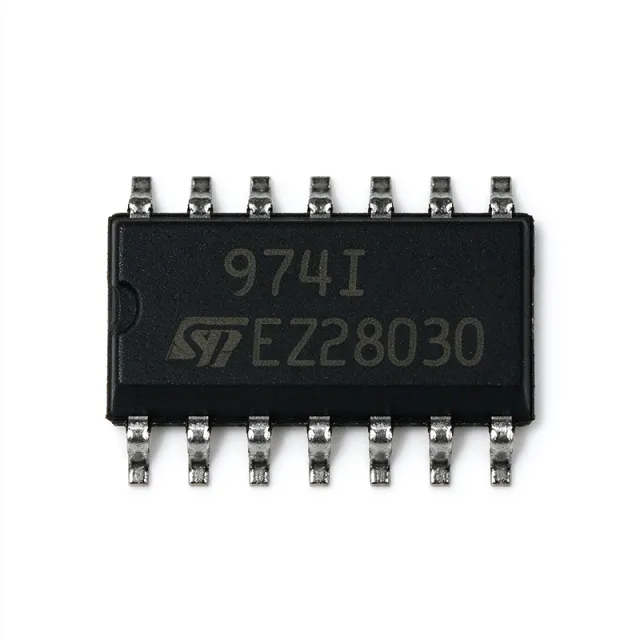
The STMicroelectronics TS944IPT is a quad CMOS-input operational amplifier delivering rail-to-rail output swing while consuming only 1.2 µA typical quiescent current per channel, packaged in a 14-pin TSSOP (Tape & Reel). It operates from a single 2.5 V to 10 V supply over the -40 °C to +85 °C industrial temperature range and provides a gain-bandwidth product of 10 kHz, making it ideal for ultra-low-power signal conditioning. An operational amplifier (op-amp) is a high-gain DC-coupled differential amplifier that uses external feedback components to set closed-loop gain, bandwidth, and transfer function. The TS944 belongs to the micropower CMOS op-amp family — a class of linear ICs that prioritize nano- to micro-amp quiescent current draw for battery-powered and energy-harvesting designs. Within the broader semiconductor hierarchy, it sits under: op-amp -> amplifier -> analog IC -> linear IC -> integrated circuit. Key features include four independent op-amp channels in one package, CMOS inputs delivering ultra-low input bias current, rail-to-rail output swing that maximizes dynamic range on low-voltage supplies, and 1.2 µA typical supply current per amplifier that enables years of runtime from small cells. The device is unity-gain stable and supports single-supply operation from 2.5 V to 10 V, simplifying designs that previously needed bipolar ±5 V rails. The TS944 architecture uses a CMOS input stage that achieves very low bias current while the class-AB output stage swings to within millivolts of both supply rails. This combination eliminates the need for input bias-current compensation in high-impedance sensor interfaces and lets designers operate the part directly from a single lithium cell or 3.3 V digital rail without sacrificing headroom. Typical applications include battery-powered sensor signal conditioning, portable medical monitors, IoT edge nodes, active filters, transducer pre-amplifiers, and any micropower analog front end where four amplifiers must fit in a small 14-pin TSSOP footprint. Designers should bypass supplies with 100 nF ceramic capacitors placed within 5 mm of VCC and avoid capacitive loads above 1 nF without an isolation resistor to prevent oscillation.

見積もり お問い合わせ
TS951ID - 3MHz Rail-to-Rail Low-Power Op Amp | STMicroelectronics
TS951ID

TS951ID - 3MHz Rail-to-Rail Low-Power Op Amp | STMicroelectronics

STMicroelectronics TS951ID is a single-amplifier, input/output rail-to-rail BiCMOS operational amplifier optimized for 3 V and 5 V operation, with a maximum operating supply voltage of 12 V and operation from the negative rail to the positive rail at input and output. The device is packaged in an 8-pin SOIC and provides approximately 3 MHz gain-bandwidth product, 1 V/µs slew rate, and 80 dB supply-voltage rejection ratio. Its low-power design targets portable instrumentation, sensor interfaces, audio signal conditioning, and general-purpose analog systems. An operational amplifier is an analog integrated circuit that amplifies the voltage difference between its inverting and non-inverting inputs while offering high input impedance, low output impedance, and stable closed-loop behavior when feedback is applied. The TS951 belongs to the operational-amplifier hierarchy, where its BiCMOS input stage combines bipolar transistor performance with CMOS power efficiency. Rail-to-rail input and output operation extends useful signal range toward the supply rails, making the amplifier practical in low-voltage systems that cannot tolerate substantial headroom loss. Key benefits include 3 MHz gain-bandwidth product for modest-frequency signal paths, 1 V/µs slew rate for faster large-signal transitions, and 80 dB supply rejection for reducing supply ripple that could otherwise modulate the amplified signal. The low-power operating approach is useful in portable equipment where energy efficiency and reduced heat generation are priorities. ESD protection rated at 2 kV adds handling robustness, while the compact SOIC-8 package supports conventional surface-mount assembly. The BiCMOS architecture is appropriate for precision and general-purpose analog blocks where low quiescent consumption and rail-to-rail signal handling are more important than high-speed performance. Because this amplifier is intended for low-power rather than high-bandwidth signal chains, applications normally use moderate feedback resistors, explicit gain-setting resistors, and stable output-loading arrangements. Its broad supply capability also permits operation from 3 V and 5 V rails, although each operating point should be checked against the complete electrical limits in the manufacturer datasheet. Typical applications include low-voltage sensor conditioning, buffered analog measurements, portable audio paths, general-purpose instrumentation, and interface buffering around higher-impedance sensors. It can also support low-frequency control or active-filter stages where the 3 MHz gain-bandwidth product provides useful bandwidth margin. In these systems, TS951ID can reduce the loading imposed on the sensor source while maintaining an output signal referenced to the available supply range. Designers should verify input common-mode range, output swing, output-current capability, noise, and stability at the intended frequency before committing the device to a new layout. Decoupling capacitors should be placed close to the supply pins, and sensitive analog inputs should be routed away from switching nodes and high-current return paths. The input and feedback networks must also avoid excessive source resistance or capacitance that could impair stability. This product data combines the verified STMicroelectronics family description, manufacturer datasheet, and distributor listings with practical guidance for package selection, sourcing, and analog layout. It also distinguishes electrically related family members from true drop-in choices and identifies unavailable pricing and lifecycle information rather than presenting unverified commercial figures.

見積もり お問い合わせ
TS951IN - 3MHz Rail-to-Rail Op Amp | STMicroelectronics
TS951IN

TS951IN - 3MHz Rail-to-Rail Op Amp | STMicroelectronics

STMicroelectronics TS951IN is a single-circuit, general-purpose BiCMOS operational amplifier featuring a 3 MHz gain-bandwidth product, a 1 V/µs slew rate, and input/output rail-to-rail operation in an 8-DIP package. The amplifier is optimized for 3 V and 5 V operation and can also operate from a supply as high as 12 V. Its low-power design consumes approximately 0.9 mA when operated from a 3 V supply, making it suitable for portable, instrumentation, sensor, and general analog signal-conditioning systems. An operational amplifier is an active analog component that amplifies the difference between its inverting and non-inverting inputs. The TS951IN belongs to the rail-to-rail operational-amplifier category and uses a BiCMOS process that combines CMOS input characteristics with bipolar output-drive capability. Rail-to-rail input common-mode range allows the amplifier to sense signals near the positive and negative supply rails, while rail-to-rail output swing improves dynamic range when the available supply voltage is limited. Key electrical characteristics include a 3 MHz gain-bandwidth product, 1 V/µs slew rate, and approximately 0.9 mA supply current at 3 V. The 3 MHz bandwidth provides useful speed for audio-frequency buffers, general-purpose signal amplification, active filters, and sensor interfaces, while the 1 V/µs slew rate permits relatively rapid output transitions. The 8-DIP package supports straightforward through-hole assembly and is suitable for prototypes, educational platforms, and applications where a larger package is acceptable. The TS951IN is built for general-purpose precision and moderate-speed analog work. Its single-amplifier configuration simplifies designs that require one independent signal path, while the low-power operating mode can reduce total system consumption in battery-powered equipment. Because a bipolar output stage is present, careful assessment of output-current capability, capacitive-load stability, and operating temperature is appropriate before assigning it to demanding loads. Typical applications include low-frequency audio buffer stages, sensor-signal conditioning, active filters, data-acquisition front ends, portable instrumentation, and general analog signal conditioning. The rail-to-rail input capability is especially useful when sensor outputs can approach either supply rail. The rail-to-rail output stage is beneficial in low-voltage systems where a conventional amplifier would clip before approaching the available output range. When designing with the TS951IN, keep feedback routing short, place compensation and decoupling components close to the device, and verify stability with the actual source impedance and load. Connect the unused input to a defined reference potential, normally the non-inverting input or a mid-supply bias point. Do not substitute a modern CMOS or rail-to-rail amplifier without checking input offset, bias-current, noise, output-drive, and supply-current differences. This page combines manufacturer family information, distributor identification, package information, and practical design guidance with a parameter comparison against same-package family alternatives. It also distinguishes the TS951IN from the TS952 and TS954 family members, whose electrical characteristics must be checked against the manufacturer datasheet before making a board-level substitution.

見積もり お問い合わせ
TS952ID - Dual 3MHz Rail-to-Rail Op Amp | STMicroelectronics
TS952ID

TS952ID - Dual 3MHz Rail-to-Rail Op Amp | STMicroelectronics

STMicroelectronics TS952ID is a dual, input/output rail-to-rail BiCMOS operational amplifier with a 3 MHz gain-bandwidth product, 1 V/us slew rate, and operation from 2.7 V to 12 V in an 8-pin SOIC package. It is optimized and specified for both 3 V and 5 V supply rails, making it suitable for low-voltage analog systems that require an amplifier to approach its supply limits at the input and output. An operational amplifier, or op amp, is a high-gain analog building block used in amplification, buffering, filtering, sensing, and feedback-control circuits. The TS952 belongs to the rail-to-rail op-amp category within the broader amplifier IC and signal-chain hierarchy. Rail-to-rail input and output behavior allows signals near either supply rail to be processed with less conventional headroom loss than a fixed-input amplifier. The TS952ID provides two amplifier circuits, a 3 MHz bandwidth, and a 1 V/us slew rate. According to the STMicroelectronics TS952 product-page data, the device is optimized for 3 V and 5 V operation. Other identified features include an 80 dB supply-voltage rejection ratio, 2 kV ESD protection, and low-power operation. These characteristics make the part applicable to low-voltage sensor conditioning, portable instrumentation, audio input stages, and general-purpose analog signal processing. The BiCMOS architecture combines bipolar input-stage behavior with CMOS output circuitry and is intended to balance low-voltage operation, amplifier performance, and power efficiency. Because the TS952 is a dual device, two independent amplifier channels can share one package. The 8-pin SOIC outline also supports conventional surface-mount assembly, although final stability, bandwidth, and output-current behavior must be evaluated at the intended supply voltage and load. Typical uses include battery-powered sensor interfaces, buffered analog inputs, portable measurement systems, audio preamplification, and low-voltage control loops. At 3 V, the device is aligned with compact battery-operated systems; at 5 V, it provides additional signal range for industrial and consumer analog circuits. The 3 MHz bandwidth is sufficient for many general-purpose conditioning stages but is not intended for high-speed video or precision wideband instrumentation without further analysis. When designing around the TS952ID, verify input and output common-mode limits, output swing, load capability, noise, offset, and stability for the selected supply voltage. Decoupling capacitors should be placed close to the supply pins, and sensitive input traces should remain short and away from switching nodes. Feedback components should follow the manufacturer recommendations because gain-bandwidth, input capacitance, and capacitive loading can affect closed-loop behavior. This product record combines the verified STMicroelectronics family description, distributor package information, operating range, bandwidth, slew rate, rejection, and ESD information with practical selection guidance. It also distinguishes verified facts from specifications that still require confirmation from the complete manufacturer datasheet, avoiding unsupported claims about electrical limits or replacement parts.

見積もり お問い合わせ
TS952IN - Dual 3MHz Rail-to-Rail Op Amp | STMicroelectronics
TS952IN

TS952IN - Dual 3MHz Rail-to-Rail Op Amp | STMicroelectronics

The STMicroelectronics TS952IN is a dual, low-power operational amplifier with input and output rail-to-rail capability, a 3 MHz gain-bandwidth product, and a 1 V/us slew rate. It operates from 2.7 V to 12 V and is packaged in an 8-pin Mini DIP. The device belongs to the TS95x family, whose BiCMOS architecture is optimized and fully specified for 3 V and 5 V operation. An operational amplifier is a voltage-controlled differential amplifier that can amplify the difference between two input voltages while providing high open-loop gain. The TS952IN contains two independent amplifier channels in one package. Rail-to-rail input operation lets each channel accept signals close to the positive or negative supply rail, while rail-to-rail output operation allows the output voltage to approach either supply limit. These characteristics make the device useful for portable instrumentation, sensor interfaces, audio paths, and low-voltage control systems. The 3 MHz gain-bandwidth product supports useful bandwidth in low-voltage signal chains without requiring a high-speed amplifier operating from a larger supply. The 1 V/us slew rate helps limit large-signal distortion when signals change quickly. Because the TS95x family is designed for low-power operation, the TS952IN is also appropriate for battery-powered equipment where a pair of independent amplifiers is useful without using two separate packages. The device is specified for a 2.7 V to 12 V supply range, with its family optimized for 3 V and 5 V systems. At low supply voltages, rail-to-rail behavior becomes especially valuable because it increases the usable input and output range relative to conventional fixed-output amplifiers. Designers should still verify the actual output swing, input common-mode range, noise, input bias current, output-current capability, and stability requirements against the manufacturer datasheet for the operating point of interest. Typical applications include buffering sensor outputs, amplifying low-level analog signals, active filtering, audio preamplification, and general-purpose signal conditioning. In a sensor interface, one channel can amplify the sensor signal while the other can provide buffering, gain, or a reference-related function. Supply bypassing, output-load compatibility, and stability with the selected feedback network are important implementation considerations for this general-purpose dual amplifier. This product page combines the verified TS952IN operating characteristics, package information, drop-in replacement findings, application guidance, and practical design notes. It is intended to help engineers identify the correct amplifier quickly, compare pin-compatible choices, and plan PCB and signal-chain changes before releasing a new design.

見積もり お問い合わせ
TS954ID - Quad 3MHz R-to-R Op Amp | STMicroelectronics
TS954ID

TS954ID - Quad 3MHz R-to-R Op Amp | STMicroelectronics

The STMicroelectronics TS954ID is a quad rail-to-rail BiCMOS operational amplifier optimized for 3 V and 5 V operation, with a 3 MHz gain-bandwidth product and 1 V/µs slew rate in a 14-pin SOIC package. The four amplifiers support supply voltages from 2.7 V to 12 V and combine low-power operation with low input bias current. An operational amplifier is an analog integrated circuit that amplifies the voltage difference between its non-inverting and inverting inputs. A rail-to-rail output amplifier can approach the supply rails at its output, making it useful when the available signal range is small. The TS954 belongs to the amplifier IC hierarchy, where operational amplifiers are used for signal conditioning, buffering, active filtering, comparisons, and analog sensor interfaces. The TS954 family provides four amplifiers per package, a 3 MHz gain-bandwidth product, and a 1 V/µs slew rate. Its input bias current is 35 nA, while the listed supply current is 950 µA per channel. These characteristics make it suitable for general-purpose signal conditioning operating from 2.7 V to 12 V, including low-voltage analog systems and battery-powered equipment. The device uses a BiCMOS input architecture combining bipolar and CMOS process characteristics. Its rail-to-rail output stage allows useful output swing near the supply limits, while the low 35 nA input bias current reduces current errors when driving high-impedance sources. The 3 MHz bandwidth is adequate for audio-frequency and general instrumentation tasks, whereas applications requiring substantially faster closed-loop settling should use a higher-bandwidth amplifier. Typical uses include low-level sensor amplification, active analog filters, audio signal conditioning, instrumentation, and four-channel buffering. The SOIC-14 package permits conventional surface-mount assembly and provides one amplifier per two package pins. Its quad configuration can also reduce board area compared with four separate single or dual amplifier packages when all four channels are required. Designers should verify the required output swing, load impedance, input common-mode range, noise performance, and stability against the manufacturer datasheet before finalizing a circuit. Decoupling capacitors should be placed close to the supply pins, and unused amplifier inputs should be biased according to the manufacturer recommendations so that input and output stages remain in their intended operating regions. This page consolidates verified manufacturer and distributor information for the TS954ID, including the 3 MHz bandwidth, 1 V/µs slew rate, 2.7 V to 12 V supply range, 14-pin SOIC format, sourcing links, and the engineering trade-offs that distinguish a low-power quad amplifier from faster or more specialized alternatives.

見積もり お問い合わせ
TS954IN - 3MHz Quad Rail-to-Rail Op Amp | STMicroelectronics
TS954IN

TS954IN - 3MHz Quad Rail-to-Rail Op Amp | STMicroelectronics

The STMicroelectronics TS954IN is a quad input/output rail-to-rail low-power BiCMOS operational amplifier optimized for 3V and 5V operation. Its four amplifiers, 3 MHz gain-bandwidth product, 1 V/us slew rate, and 14-DIP package make it suitable for compact analog signal-conditioning systems requiring low-voltage supply operation. The input and output stages support rail-to-rail signal handling, while the 80 dB supply-voltage rejection specification helps suppress supply-related signal distortion. An operational amplifier is an active semiconductor device that amplifies the voltage difference between its differential inputs. Rail-to-rail input capability means the input common-mode range can extend toward both supply rails, while rail-to-rail output capability allows the output voltage to approach the operating limits more closely than a conventional non-rail-to-rail amplifier. The TS954IN belongs to the TS95x family of low-power BiCMOS operational amplifiers optimized for single-supply systems. Key characteristics include four amplifier channels in one package, a 3 MHz gain-bandwidth product, and a 1 V/us slew rate. These specifications support applications such as sensor interfaces, buffered analog signals, low-voltage instrumentation, audio paths, and general-purpose analog conditioning. The TS954IN is also identified as ESD protected to 2 kV and includes latch-up protection according to the manufacturer datasheet information. The BiCMOS architecture combines bipolar input characteristics with CMOS power-handling behavior. This implementation supports low-power operation while maintaining a useful small-signal bandwidth for sensor, filtering, and signal-buffer circuits. At a 3V supply, the family is specifically optimized for low-power consumption, which makes it relevant to portable equipment and embedded analog systems that cannot justify a higher-power precision amplifier. Typical uses include buffering sensor outputs, amplifying low-level analog signals, active filtering, level shifting, audio preamplification, and instrumentation. The quad organization reduces package count when several independent analog channels are required. Designers should still evaluate input offset voltage, input bias current, output-current capability, noise, and stability for the exact gain, load, and supply conditions before finalizing a circuit. The principal design consideration is operating margin. Rail-to-rail inputs and outputs do not remove the requirement to maintain adequate input and output voltage limits, especially under load. Decoupling capacitors should be placed close to the supply pins, and feedback networks should be designed to preserve the intended closed-loop gain while avoiding output saturation. This product page combines the manufacturer family description with practical application guidance, parameter comparison, and pin-package considerations. It is intended to help engineers determine whether the TS954IN's four-channel 3V/5V rail-to-rail architecture fits a board-level design before consulting the complete manufacturer datasheet for limit values and test conditions.

見積もり お問い合わせ
TS971ID - 12MHz Low-Noise Rail-to-Rail Op Amp | STMicroelectronics
TS971ID

TS971ID - 12MHz Low-Noise Rail-to-Rail Op Amp | STMicroelectronics

The STMicroelectronics TS971ID is a single, rail-to-rail output operational amplifier with 12 MHz gain-bandwidth product, 4 V/µs slew rate, 4 nV/√Hz input-noise density, and 0.003% ultra-low distortion. The device operates from 2.7 V to 10 V and is supplied in an 8-pin SOIC package. Its combination of low noise, high gain bandwidth, rail-to-rail output swing, and wide supply range makes it suitable for portable audio, instrumentation, sensor conditioning, and general-purpose signal-processing circuits. An operational amplifier is an analog integrated circuit that amplifies the difference between two input voltages. The TS971ID belongs to the operational-amplifier hierarchy within analog and mixed-signal ICs. Rail-to-rail output means the output can swing close to either supply rail, improving usable output range in low-voltage systems. The single-amplifier configuration also keeps the package compact for cost-sensitive designs requiring one precision analog channel. The principal performance features include 12 MHz gain bandwidth and a 4 V/µs slew rate, allowing the amplifier to process relatively fast signals without excessive settling limitations. Input-noise density is specified at 4 nV/√Hz, and the listed distortion is 0.003%. According to the STMicroelectronics product family information, TS97x devices can operate with supply voltages as low as ±1.35 V and are intended for portable and battery-powered equipment. The TS971ID combines rail-to-rail output operation with low-noise and low-distortion behavior. ESD protection is listed at 2 kV, while latch-up immunity is identified as Class A. These characteristics are particularly useful when a circuit must preserve small-signal information while operating from a constrained supply. The amplifier's 2.7 V to 10 V operating range supports conventional 3.3 V, 5 V, and up-to-10 V system rails. Typical uses include microphone and line-level audio preamplification, portable measurement equipment, low-level sensor interfaces, active filters, and buffered sensor outputs. In an audio preamplifier, the 4 nV/√Hz noise density helps limit the amplifier's contribution to the system noise floor. In instrumentation, the 12 MHz bandwidth provides useful signal range, while the 0.003% distortion specification supports high-fidelity signal paths. When designing a TS971ID circuit, verify the input and output common-mode limits, operating-voltage range, output-current capability, and stability requirements against the manufacturer datasheet. Place input, output, and compensation-network components close to the device, and use a suitable output-load arrangement. Because the verified search results do not provide a public price or a complete manufacturer pin table, those details are not inferred here.

見積もり お問い合わせ
TS972ID - 12 MHz Dual Rail-to-Rail Low-Noise Op Amp | STMicroelectronics
TS972ID

TS972ID - 12 MHz Dual Rail-to-Rail Low-Noise Op Amp | STMicroelectronics

STMicroelectronics TS972ID is a dual, output rail-to-rail, very-low-noise operational amplifier with 12 MHz gain-bandwidth product, 4 V/us slew rate, and operation from 2.7 V to 10 V in an 8-pin SOIC package. Its principal characteristics are 4 nV/Hz noise density, 0.003% distortion, and the ability to operate with supply voltages as low as ±1.35 V. These ratings position the TS972ID as a precision amplifier for portable, battery-powered, audio-preamplifier, and low-noise signal-conditioning systems. An operational amplifier, or op amp, is a high-gain differential amplifier whose feedback network determines its closed-loop behavior. Within the integrated-circuit hierarchy, the TS972ID belongs to the operational-amplifier class, amplifier IC category, and broader analog and mixed-signal semiconductor family. Rail-to-rail output capability lets its output approach the supply rails more closely than a conventional amplifier, improving usable output swing in compact low-voltage systems. The TS972ID combines three defining benefits: 12 MHz gain-bandwidth product for moderate-frequency amplification, 4 V/us slew rate for faster signal transitions, and 4 nV/Hz input-voltage noise for low-noise operation. A 0.003% distortion figure further supports high-fidelity signal paths. The dual configuration provides two amplifiers in one 8-pin SOIC, reducing board area compared with two separate single-channel packages. Its low-voltage operating range and rail-to-rail output architecture suit systems that cannot tolerate the headroom required by conventional amplifiers. The 2.7 V to 10 V supply specification permits operation from a single 3.3 V rail, dual ±2.5 V rails, or other compatible supplies. The manufacturer description specifically identifies portable and battery-powered equipment as suitable markets, while the noise and distortion specifications make audio preamplification a natural fit. Typical uses include portable audio preamplifiers, low-noise sensor conditioning, microphone stages, active filters, and buffered sensor outputs. Two amplifiers in one package can implement dual signal channels, instrumentation front ends, or complementary gain stages when their independent inputs and outputs are required. Care is still necessary when driving capacitive loads, observing output-current limits, and controlling stability around the amplifier and feedback network. The primary design consideration is stable implementation of the intended gain. Input and feedback resistances should be selected consistently with the 12 MHz bandwidth and noise target, while board layout should minimize parasitic capacitance and feedback-loop coupling. Decoupling capacitors should be placed close to the supply pins, and unused amplifier channels should be configured according to the manufacturer guidance rather than left floating. This page consolidates the verified TS972ID operating limits, source references, and same-family alternatives with practical selection and layout guidance. It distinguishes documented facts from parameters requiring confirmation, making the result more useful for PCB compatibility reviews, sourcing, and amplifier design decisions.

見積もり お問い合わせ
TS972IN - Dual Low-Noise R2R Op Amp | STMicroelectronics
TS972IN

TS972IN - Dual Low-Noise R2R Op Amp | STMicroelectronics

STMicroelectronics TS972IN is a dual operational amplifier with rail-to-rail output swing, very low noise of 4 nV/Hz, 12 MHz gain-bandwidth product, and 4 V/us slew rate. The device operates from dual supplies as low as ±1.35 V and is packaged for through-hole assembly in an 8-DIP package with 7.62 mm pin spacing. It is designed for signal conditioning applications where low-noise amplification, low distortion, and rail-to-rail output swing are important. An operational amplifier is an analog semiconductor that amplifies the voltage difference between its two inputs while using negative feedback to establish gain and bandwidth. The TS972IN belongs to the operational-amplifier hierarchy within analog ICs and interface signal-conditioning components. Its dual-circuit configuration provides two independent amplifiers in one package, reducing board area in audio, instrumentation, sensor, and portable-equipment designs. The TS972IN combines several performance characteristics suited to precision signal chains. Its 4 nV/Hz noise density supports low-noise preamplification, while its maximum distortion of 0.003% is useful in audio and measurement paths. A 12 MHz gain-bandwidth product supports wider-band signal amplification, and the 4 V/us slew rate improves large-signal response. Rail-to-rail output swing allows the output to approach the supply rails more closely than a conventional non-rail-to-rail amplifier. The TS97x family supports operation from voltages as low as ±1.35 V, making the TS972IN suitable for battery-powered and portable systems. Its specified operating range extends to 10 V. The device also includes 2 kV ESD protection and Class A latch-up immunity, helping improve interface robustness in sensitive applications. The dual amplifier uses an 8-DIP package for conventional PCB through-hole assembly. Typical uses include audio preamplification, portable instrumentation, low-level sensor conditioning, active filtering, and general-purpose analog signal conditioning. Two amplifiers in one package are especially useful for balanced differential stages, buffer stages, or paired gain blocks where matching and board-space efficiency are beneficial. Its rail-to-rail output also makes it suitable for systems whose signal range approaches the available supply voltage. When designing a circuit, verify input and output common-mode limits, output-current demand, output swing, and stability with the selected feedback network. Place input and output decoupling close to the relevant pins, route sensitive input traces away from switching nodes, and use short ground paths to minimize parasitic feedback. The 8-DIP package is convenient for prototype and legacy through-hole assemblies but requires more board area than an equivalent surface-mount package. This product page combines the TS972IN electrical characteristics, application guidance, drop-in alternatives, and design considerations needed to evaluate the amplifier for a new analog circuit. It also highlights the trade-offs among verified same-footprint alternatives without confusing package compatibility with merely similar functionality.

見積もり お問い合わせ
TS974ID - 12 MHz Low-Noise Rail-to-Rail Op Amp | STMicroelectronics
TS974ID

TS974ID - 12 MHz Low-Noise Rail-to-Rail Op Amp | STMicroelectronics

The STMicroelectronics TS974ID is a quad operational amplifier with four rail-to-rail output stages, 12 MHz gain-bandwidth product, 4 V/µs slew rate, and 4 nV/√Hz noise density in a 14-pin SOIC package. It operates from 2.7 V to 10 V, including split-supply operation as low as ±1.35 V, and is intended for portable, battery-powered, audio, sensor, and general-purpose signal-conditioning systems. An operational amplifier is an analog integrated circuit that uses high-gain differential feedback to amplify small voltage signals. The TS974ID belongs to the TS97x family of low-noise, low-distortion amplifiers. Within the broader semiconductor hierarchy, an operational amplifier is an analog amplifier IC, a linear signal-processing component, and ultimately part of a power-management and signal-chain ecosystem. Its four amplifiers combine rail-to-rail output swing with a 12 MHz bandwidth and 4 V/µs slew rate. The stated 4 nV/√Hz noise density supports low-noise signal acquisition, while the specified 0.003% distortion improves linearity in audio and precision analog circuits. A supply range of 2.7 V to 10 V permits operation from a single 3.3 V or 5 V rail or from a split supply as low as ±1.35 V. The TS97x architecture is designed for low-noise and low-distortion performance, with particular suitability for portable and battery-supplied equipment. The quad configuration provides four amplifiers in one 14-pin SOIC package, reducing board area when multiple analog channels require similar electrical performance. Its 12 MHz bandwidth is substantially higher than that required for many slow sensor-conditioning channels, allowing designers to preserve signal fidelity over a wider frequency range. Typical applications include audio preamplification, microphone and sensor conditioning, portable instrumentation, active filtering, data acquisition, and low-voltage embedded systems. The TS974ID is especially useful when several channels must process signals without adding a separate amplifier package for every stage. In audio systems, its low noise and low distortion support cleaner preamplifier operation; in sensors, the rail-to-rail output can improve usable dynamic range on low-voltage supplies. When designing around the TS974ID, account for input common-mode range, output swing, stability with the selected feedback network, and noise bandwidth. Decoupling capacitors should be placed close to the supply pins, while analog input and feedback paths should be kept short and away from switching nodes. Stable feedback components and suitable output loading are important when exploiting the device's 12 MHz bandwidth. This product record consolidates verified manufacturer-family characteristics, distributor availability, package information, and practical application guidance. It also identifies the missing pricing, pin-level, environmental, and qualification details explicitly rather than estimating them, allowing engineers to compare the TS974ID against other low-noise rail-to-rail quad amplifiers before committing to a design.

USD $1.23 在庫あり
TS974IN - 4-Channel Low-Noise Rail-to-Rail Op Amp | STMicroelectronics
TS974IN

TS974IN - 4-Channel Low-Noise Rail-to-Rail Op Amp | STMicroelectronics

The STMicroelectronics TS974IN is a four-circuit, rail-to-rail operational amplifier with a very low noise density of 4 nV/Hz, a 12 MHz gain-bandwidth product, and a 4 V/us slew rate, packaged in a 14-pin DIP. It is designed for applications that require low-noise signal amplification across multiple independent channels. An operational amplifier is an analog integrated circuit that amplifies the voltage difference between its non-inverting and inverting inputs. Within the amplifier hierarchy, the TS974IN is a general-purpose precision operational amplifier and a member of the rail-to-rail low-noise amplifier family. Rail-to-rail input and output operation allows the signal to approach the supply rails, improving usable dynamic range in low-voltage and single-supply systems. The TS974IN provides four amplifier channels in one package, reducing board area and simplifying multi-channel signal-conditioning layouts. Its 4 nV/Hz noise density supports high-resolution analog measurement, while the 12 MHz gain-bandwidth product and 4 V/us slew rate preserve signal fidelity in faster signal paths. The listed ultra-low distortion of 0.003% makes the device suitable for audio preamplification, filtering, buffering, and instrumentation. The device operates over a supply range extending to 10 V and includes ESD protection rated at 2 kV. The listed latch-up immunity is Class A. Each amplifier is configured as a standard voltage-feedback operational amplifier, allowing the same component to implement inverting, non-inverting, summing, comparator-style, and active-filter circuits. Operating and electrical limits should always be confirmed in the manufacturer datasheet. Typical uses include four-channel audio preamplification, sensor signal conditioning, active audio filters, low-level instrumentation, data acquisition front ends, and general-purpose analog buffering. Because all four channels share one package, matching and thermal tracking are convenient when several related analog signals are processed under similar conditions. For low-noise layouts, keep the input and feedback resistors short, place input compensation and decoupling capacitors close to the relevant pins, and avoid routing high-impedance input traces beside digital clock or switching nodes. Select the bypass capacitance and compensation values with the datasheet's stability and noise guidance in mind, particularly when driving capacitive loads. This page combines the verified TS974IN product characteristics with application guidance, drop-in replacement analysis, and engineering design notes. It is intended to help designers evaluate the TS974IN quickly while completing the mandatory signal-integrity, noise, and stability checks against the full manufacturer documentation.

見積もり お問い合わせ
TSA1005-40IFT - 10-Bit 40MSPS Dual ADC | STMicroelectronics
TSA1005-40IFT

TSA1005-40IFT - 10-Bit 40MSPS Dual ADC | STMicroelectronics

The STMicroelectronics TSA1005-40IFT is a dual-channel, 10-bit resolution analog-to-digital converter (ADC) based on a pipelined architecture, sampling up to 40 MSPS in a 48-pin TQFP (7x7 mm) package. It uses a 0.25 µm deep sub-micron CMOS process, operates from a single 2.5 V analog supply, and supports an independent 2.5 V or 3.3 V CMOS output supply. A pipelined ADC is a high-speed converter architecture that resolves an analog input across multiple cascaded low-resolution stages, each driving a sample-and-hold amplifier and a flash sub-ADC. The pipeline allows new conversions to begin every clock cycle, achieving sample rates well above 100 MSPS while keeping per-stage hardware compact. Pipelined ADCs sit within the broader taxonomy: data converter -> ADC -> high-speed ADC -> pipelined ADC -> integrated circuit -> semiconductor. The TSA1005 belongs to a category often called "baseband IF sampling ADCs," used when analog signals need to be digitized near the antenna or sensor for downstream DSP. Key specifications include 1 GHz analog input bandwidth, an integrated track-and-hold amplifier per channel, common clocking for synchronous dual-channel sampling, and a multiplexed digital output mode. The device targets applications needing a low noise floor and high SFDR; SFDR (Spurious-Free Dynamic Range) measures how far the largest spurious tone sits below the fundamental when digitizing a pure sine wave, with higher values meaning cleaner spectra. The TSA1005 is engineered for very low noise floor, high SFDR, and good channel-to-channel isolation. Typical applications include medical ultrasound imaging, professional video processing, IF (intermediate frequency) sampling for communications receivers, instrumentation, and industrial non-destructive testing. Each application relies on the part's combination of 10-bit resolution at video-grade sample rates and dual-channel synchronous capture. When designing with this part, decouple both the 2.5 V analog and 2.5/3.3 V digital rails with 100 nF ceramic capacitors placed as close as possible to each supply pin. Route the analog inputs as 50 Ω controlled-impedance traces with the analog ground plane isolated from the digital return to minimize coupling. This page synthesizes distributor pricing, drop-in same-package alternatives, and practical PCB layout notes not found in the manufacturer datasheet alone. Information current as of 2026-10-15.

見積もり お問い合わせ
TSA1203IF - Dual 12-bit 40MSPS ADC | STMicroelectronics
TSA1203IF

TSA1203IF - Dual 12-bit 40MSPS ADC | STMicroelectronics

The STMicroelectronics TSA1203IF is a dual-channel, 12-bit, 40 MSPS analog-to-digital converter fabricated in a mainstream 0.25 µm CMOS process, housed in a 48-pin TQFP (7x7 mm) package. It integrates two simultaneous sample-and-hold amplifiers, a 1 GHz analog input bandwidth, and a built-in reference voltage, dissipating 230 mW at 40 Msps from a single 2.5 V supply. The CMOS output stage can be driven from an independent 2.5 V or 3.3 V rail, simplifying interfacing to both legacy and modern FPGA/ASIC logic families. An analog-to-digital converter (ADC) is a mixed-signal integrated circuit that converts a continuous-time, continuous-amplitude analog input into a discrete-time, discrete-amplitude digital code. Pipeline ADCs such as the TSA1203IF use a multi-stage switched-capacitor architecture to achieve high sampling rates while keeping per-stage power and die area modest, sitting within the broader hierarchy of data converters -> ADC -> high-speed pipeline ADC -> semiconductor. Dual-channel variants like this one are favored for diversity receivers, I/Q baseband sampling, and simultaneous multi-antenna digital beamforming because the two channels are sampled on a common clock edge, eliminating channel-to-channel skew. Key features include 1 GHz analog input bandwidth, SFDR of -68.3 dBc at 10 MHz input, multiplexed outputs for reduced pin count, common clocking between channels, and pin-to-pin compatibility with the dual 10-bit 20/40 MSPS TSA1005-20/40 and the dual 12-bit 20 MSPS TSA1204. The pipelined architecture combined with digital error correction yields clean 12-bit outputs at full clock rate without requiring complex external calibration at room temperature. Typical applications include cellular base station receivers, IF sampling for software-defined radio, medical imaging front-ends, and industrial ultrasound beamformers. The integrated reference and dual independent input channels also suit multi-channel data-acquisition cards for test and measurement instrumentation. When designing with this part, ensure the analog and digital grounds are joined only at a single point near the exposed pad, and that the analog supply is decoupled with both 0.1 µF ceramic and 10 µF bulk capacitance within 5 mm of the supply pins.

見積もり お問い合わせ
TSA1204IFT - 12-Bit 20MSPS Dual-Channel ADC | STMicroelectronics
TSA1204IFT

TSA1204IFT - 12-Bit 20MSPS Dual-Channel ADC | STMicroelectronics

The STMicroelectronics TSA1204IFT is a 12-bit resolution, dual-channel pipelined Analog-to-Digital Converter sampling up to 20 MSPS, packaged in a 48-pin TQFP (7x7 mm). The device operates from a single 2.5 V analog supply with an independent 2.5 V/3.3 V CMOS output stage supply, consuming only 95 mW per channel at 20 MSPS and scaling down adaptively at lower sampling rates. An Analog-to-Digital Converter (ADC) is a mixed-signal integrated circuit that converts continuous-time analog voltages into discrete digital codes at a specified sampling rate. Dual-channel pipelined ADCs belong to the broader hierarchy of data converter IC -> mixed-signal IC -> semiconductor, and they occupy the performance tier between successive-approximation (SAR) converters (slow, low-power, <5 MSPS) and high-speed flash converters (very fast, very high power). The TSA1204IFT targets moderate-bandwidth multi-channel systems where engineers need two synchronized channels without the cost of two discrete ADCs. Key features include a 1 GHz analog input bandwidth, an integrated Track-and-Hold amplifier, 11.2-bit effective number of bits (ENOB) at the Nyquist input frequency, and -81.5 dBc spurious-free dynamic range (SFDR) at Nyquist. The 0.25 micrometer CMOS process enables adaptive power consumption scaling from 0.5 MSPS to 20 MSPS, allowing the part to drop to lower power in standby. The CMOS outputs are pin-selectable between 2.5 V and 3.3 V logic levels, simplifying interface to FPGAs, ASICs, or microcontrollers in mixed-voltage systems. Typical applications include dual-channel digital oscilloscopes, intermediate-frequency (IF) signal processing in communications receivers, ultrasound imaging front-ends, and high-speed industrial data acquisition. The dual channel allows simultaneous sampling of in-phase and quadrature (I/Q) baseband signals, or two channels of a multi-channel instrumentation system. When designing with the TSA1204IFT, place the analog and digital ground returns on a split ground plane joined under the ADC, use wide PCB traces for the analog supply pins, and decouple each supply pin with 100 nF and 10 uF capacitors placed as close as possible to the device. The exposed pad of the TQFP should be soldered to a ground plane for thermal and electrical performance. This page synthesizes distributor pricing, drop-in same-family alternatives, and practical design notes not collected in any single manufacturer datasheet revision, giving engineers a one-stop reference for sourcing and second-sourcing the TSA1204IFT.

見積もり お問い合わせ
TSA1401IF - 14-bit 20MSPS 85mW ADC | STMicroelectronics
TSA1401IF

TSA1401IF - 14-bit 20MSPS 85mW ADC | STMicroelectronics

The STMicroelectronics TSA1401IF is a 14-bit, 20 MSPS pipelined analog-to-digital converter that consumes only 85 mW at full sampling rate. Housed in a 48-pin TQFP (7x7 mm) package, the part targets low-power imaging and instrumentation applications where conventional 14-bit ADCs exceed the system thermal budget. According to the STMicroelectronics datasheet, the TSA1401IF implements ST's OPTIMWATT architecture to dynamically scale internal bias currents with clock rate, enabling designers to lower the sampling clock for slower channels and reduce overall system power. An ADC (analog-to-digital converter) is a mixed-signal integrated circuit that quantizes a continuous-time analog input into a discrete N-bit binary code at a programmable sample rate. TSA1401IF sits in the high-speed, mid-resolution segment of the ADC taxonomy (ADC -> pipelined ADC -> high-speed ADC -> data converter -> mixed-signal IC). Pipelined ADCs use multiple low-resolution flash stages interleaved with residue gain and digital correction to achieve both high conversion rate and moderate resolution; this architecture dominates the 10-100 MSPS / 10-14 bit space used in CCD imaging, ultrasound front ends, and digital oscilloscope channels. Key specifications include 14-bit resolution, 20 MSPS maximum sample rate, 85 mW typical power dissipation at full speed, single 5 V analog supply, single +3 V to +5 V digital supply, 48-pin TQFP (7x7 mm) package, industrial temperature range (-40 C to +85 C), and an external reference input. The pipelined converter includes self-calibrated digital error correction that typically holds DNL within 0.5 LSB and INL within 1.0 LSB across the industrial temperature range. Differential analog inputs are AC-coupled through on-chip clamp protection, supporting full-scale ranges from 1 Vp-p to 2 Vp-p driven by op-amp or transformer front ends. Typical applications include high-end infrared imaging for surveillance and thermography, X-ray medical imaging front ends, professional CCD camera front ends for broadcast and industrial vision, document scanners and digital copiers, and test instrumentation including digital storage oscilloscopes and arbitrary waveform recorders. Designers value the TSA1401IF in battery-powered portable imaging systems where total BOM power directly limits field runtime. When designing with the TSA1401IF, the analog input must be driven from a low-impedance differential source; designers typically use a transformer (for single-ended to differential conversion) or a fully-differential op-amp such as the THS4503. Decoupling must include 10 uF tantalum plus 100 nF ceramic on each supply pin, placed within 5 mm of the package. The clock line should be routed with 50 ohm controlled impedance and kept away from analog signal traces. This page synthesizes distributor pricing, identical-footprint drop-in alternatives from the same STMicroelectronics family, and practical layout notes that complement the official datasheet.

見積もり お問い合わせ
TSA7887ARMZ - 12-Bit 125ksps 2-Ch SAR ADC | Silicon Labs
TSA7887ARMZ

TSA7887ARMZ - 12-Bit 125ksps 2-Ch SAR ADC | Silicon Labs

The Silicon Labs TSA7887ARMZ is a 12-bit, 125 ksps, 2-channel successive-approximation register (SAR) analog-to-digital converter with a serial SPI/QSPI/MICROWIRE-compatible output, an internal 2.5V reference, and an 8-pin MSOP package. Originally developed by Touchstone Semiconductor (later acquired and second-sourced by Silicon Labs), the device operates from a 2.7V to 5.25V analog supply and is targeted at low-power instrumentation that demands sub-microamp standby current and 12-bit true conversion precision. An SAR ADC (successive-approximation-register analog-to-digital converter) is a type of data converter that uses a binary-search algorithm against an internal capacitive DAC to resolve an analog input one bit per conversion clock cycle. It belongs to the broad family of analog-to-digital converters (ADCs), which itself is part of the data-converter hierarchy inside mixed-signal and signal-chain integrated circuits. The SAR architecture is favored over delta-sigma and pipeline ADCs when low-latency deterministic conversion, small package size, and moderate sample rates (tens to hundreds of ksps) are required, particularly in multiplexed multi-channel systems. Key features of the TSA7887ARMZ include an internal 2.5V reference (selectable externally via the REF pin), a 2-channel analog input multiplexer, true 12-bit performance with no missing codes, a 125 ksps maximum throughput, low power dissipation (typically under 2.5 mW at 3V/100 ksps), and automatic power-down between conversions that drops supply current below 1 microampere. The device uses an external clock for the serial interface and supports both unipolar single-ended and pseudo-differential input configurations. The device leverages a charge-redistribution SAR core with input transient suppression and an automatic input common-mode settling window, which makes it tolerant of source-impedance variations when channels are switched. Combined with the internal precision reference, this means the TSA7887ARMZ can replace an external ADC + reference + op-amp buffer chain in many space-constrained designs. Typical applications include portable and battery-powered data loggers, industrial process-control sensor front-ends (thermocouple, RTD, strain-gauge bridges), handheld instrumentation, and multiplexed 4-20 mA loop monitors. Designers also use it in optical sensor modules and consumer battery chargers where periodic current/voltage telemetry is required. When designing with this part, size the input RC network and reference bypass capacitors per the datasheet's application circuit - inadequate decoupling is the most common cause of last-2-LSB noise and gain drift in SAR circuits. Consider the MAX1276CTC+ from Maxim's family as a drop-in 8-pin MSOP alternative if higher conversion speed is needed. This page synthesizes distributor pricing, drop-in MSOP-8 alternatives, and practical design notes not found in the manufacturer datasheet alone.

見積もり お問い合わせ
TSA7887ARMZ-REEL - 12-bit 125ksps 2-ch SAR ADC | Silicon Labs
TSA7887ARMZ-REEL

TSA7887ARMZ-REEL - 12-bit 125ksps 2-ch SAR ADC | Silicon Labs

The Silicon Labs TSA7887ARMZ-REEL is a 12-bit, 125 ksps, 2-channel successive-approximation-register (SAR) analog-to-digital converter housed in an 8-pin MSOP package with a single +2.7V to +5.25V supply. The 'RMZ' suffix indicates the MSOP-8 (RM) tape-and-reel (REEL) packaging variant. Originally designed by Touchstone Semiconductor as a pin-compatible second source for the ADI AD7887, the part features an internal +2.5V reference, internal wideband track-and-hold, and serial I/O compatible with SPI, MICROWIRE, QSPI, and DSP ports. Typical supply current is 0.85 mA at full throughput, qualifying the part as a micropower converter for battery and loop-powered systems. A SAR ADC is a successive-approximation-register analog-to-digital converter, a converter topology that uses a binary-search algorithm and a capacitive charge-redistribution DAC to resolve each conversion in N clock cycles for an N-bit result. SAR converters sit in the data-converter hierarchy between flash converters (fastest, lowest resolution) and sigma-delta converters (highest resolution, slowest). They are valued for deterministic latency, low power consumption, and the ability to drive them directly from a microcontroller or DSP serial port without an external reference or high-speed clock. Key features include a 500 ns input track-and-hold acquisition time, an internal +2.5V reference that eliminates external reference components, and a single-ended analog input structure that supports one or two channels multiplexed to the ADC core. Throughput scales with the external serial clock up to 125 ksps at 2 MHz SCLK. The wide supply range allows direct interfacing to 3.3V and 5V microcontrollers, while the small MSOP-8 footprint suits space-constrained sensor readouts and portable instrumentation. Typical applications include transducer and sensor signal conditioning, battery-powered data loggers, industrial process control loops with 4-20 mA interfaces, and portable medical or instrumentation front-ends. The combination of low power, internal reference, and small footprint also suits loop-powered 4-20 mA smart transmitters where every milliwatt and square millimeter matters. When designing with this device, ensure the analog input stays within the input common-mode range specified by the supply, and add a small RC anti-alias filter on each input to limit out-of-band noise folding into the conversion result.

見積もり お問い合わせ
TSA7887ARZ - 12-bit 125ksps 2-ch SAR ADC | Silicon Labs SOIC-8
TSA7887ARZ

TSA7887ARZ - 12-bit 125ksps 2-ch SAR ADC | Silicon Labs SOIC-8

The Silicon Labs TSA7887ARZ is a micropower, 2-channel, 125-ksps, serial-output 12-bit successive-approximation analog-to-digital converter housed in an 8-pin SOIC (RZ) package. It integrates a precision 2.5V internal reference, supports a single 2.7V to 5.25V analog supply, and consumes only 3.2 mW at 125 ksps with full power-down modes reducing quiescent current to sub-microamp levels. The part accepts true bipolar input ranges via flexible reference configuration. An ADC (analog-to-digital converter) is a data-acquisition integrated circuit that samples continuous analog voltages and converts each sample into a discrete digital code for processing by a microcontroller, DSP, or FPGA. Successive-approximation-register (SAR) ADCs use a binary-search algorithm against a precision DAC and reference to resolve one bit per clock cycle, achieving a deterministic conversion time of N cycles for N-bit resolution. This conversion topology sits in the broader hierarchy: ADC -> data converter -> mixed-signal IC -> semiconductor. SAR ADCs are prized for low latency, deterministic behavior, and absence of pipeline-latency artifacts. Key features include 12-bit resolution with no missing codes, an integrated 2.5V reference, an SPI-/QSPI-/MICROWIRE-compatible serial interface, true-differential analog inputs, software-configurable unipolar/bipolar input ranges, and a hardware-power-down pin. The internal reference can be overdriven with an external source, simplifying ratiometric measurements such as bridge-sensor readings. An on-chip oscillator eliminates the need for an external clock source in cost-sensitive designs. Architecturally, the TSA7887ARZ uses a charge-balancing switched-capacitor DAC front end that converts the input voltage into a digital code across 12 SAR clock cycles. The auto-calibration cycle corrects offset and gain errors on every conversion, eliminating drift across temperature and supply variations. Serial data is clocked out MSB-first and conforms to standard SPI modes, allowing direct connection to most modern microcontrollers without glue logic. Typical applications include portable instrumentation, battery-powered data loggers, industrial process-control loops, sensor conditioning modules, and panel-meter front ends. The low power draw makes it particularly attractive for solar- or energy-harvesting systems where average current budget is critical. The integrated reference and 2-channel mux further reduce total BOM and PCB area in compact designs. When designing with this part, ensure the analog supply is decoupled with a 1uF ceramic plus a 10uF bulk capacitor placed within 5 mm of the AVDD pin. Reference-pin decoupling is equally critical - a 0.1uF ceramic directly across REF should be used. Avoid switching digital traces under the analog front end to preserve SNR. This page synthesizes distributor pricing, drop-in alternatives, and practical design notes not found in the manufacturer datasheet alone.

見積もり お問い合わせ
TSA7887ARZ-REEL - 12-bit 125ksps 2-ch SAR ADC SOIC-8 | Silicon Labs
TSA7887ARZ-REEL

TSA7887ARZ-REEL - 12-bit 125ksps 2-ch SAR ADC SOIC-8 | Silicon Labs

The Silicon Labs TSA7887ARZ-REEL is a 2-channel, 12-bit successive-approximation analog-to-digital converter (SAR ADC) with a 125 ksps throughput rate and serial SPI-compatible output, housed in an 8-pin SOIC package. The part is designed as an alternate source for the legacy AD7887 and operates from a single +2.7 V to +5.25 V supply while drawing only 0.85 mA typical supply current, supporting micropower applications. An integrated 2.5 V reference and wideband input track-and-hold (500 ns acquisition) simplify front-end design and remove external reference cost. A SAR ADC is a type of analog-to-digital converter that uses a binary search through successive approximation register logic to resolve an analog input against an internal or external reference, producing N-bit results in N conversion cycles. SAR ADCs excel at medium-to-high resolution (12-18 bit) sampling at moderate speeds (10 ksps to 10 Msps) without the pipeline latency of higher-speed flash or pipelined architectures, making them ideal for multiplexed multi-channel data acquisition systems. Within the data-converter hierarchy, the TSA7887ARZ-REEL sits as a precision ADC -> data converter -> signal chain IC -> mixed-signal semiconductor, combining analog input conditioning, reference generation, and digital serial interface on a single die. Key features include a 125 ksps maximum sampling rate, two single-ended analog input channels multiplexed into one ADC core, an internal 2.5 V reference, a low 0.85 mA supply current, a wide input bandwidth track-and-hold (500 ns), and a serial interface compatible with SPI/QSPI/MICROWIRE. The device accepts bipolar-input-capable front end via simple resistor networks and provides an external reference option when system-level drift compensation is required. The 8-pin SOIC footprint supports standard surface-mount assembly flows. Architecturally, the TSA7887ARZ-REEL uses a charge-redistribution DAC array with successive-approximation register logic clocked from an external serial clock up to 2 MHz. The wideband track-and-hold preserves signal fidelity above the Nyquist limit of the 125 ksps sampling rate, while the integrated reference and input MUX eliminate the external analog conditioning typically required for discrete ADC designs. The serial output reduces pin count versus parallel-output ADCs and simplifies galvanic isolation in industrial systems. Typical applications include portable battery-powered instrumentation, industrial process-control loop monitoring, multi-channel data-logger front ends, sensor-signal conditioning for strain-gauge and thermocouple inputs, and touch-screen / resistive-position decoder interfaces. The low 0.85 mA supply current also suits remote or solar-powered sensor nodes. Where higher throughput is needed, the part's SPI-compatible daisy-chain capability lets two devices share a single serial port. When designing with this device, drive the analog inputs from low-impedance buffers (<= 50 ohm source impedance) to avoid conversion errors caused by the kick-back charge of the internal CDAC array. Bypass VDD with a 0.1 uF ceramic plus 10 uF tantalum placed within 5 mm of the supply pin, and provide a clean analog ground return to keep the integrated reference stable. The throughput scales linearly with external SCLK; a 2 MHz SCLK yields the rated 125 ksps. Note that the TSA7887ARZ-REEL is currently listed as obsolete by Silicon Labs (last-time-buy status), so long-life designs should consider the newer AD7887SRZ-EP equivalent. This page synthesizes distributor pricing, drop-in alternatives, and practical design notes not found in the manufacturer datasheet alone.

見積もり お問い合わせ
TSA7887BRZ - 12-bit 125kSPS 2-Ch SAR ADC | Silicon Labs
TSA7887BRZ

TSA7887BRZ - 12-bit 125kSPS 2-Ch SAR ADC | Silicon Labs

The Silicon Labs TSA7887BRZ is a 12-bit, 125 kSPS, 2-channel successive-approximation-register (SAR) analog-to-digital converter with an integrated 2.5 V internal reference, housed in an 8-pin SOIC package. It operates from a single 2.7 V to 5.25 V analog supply and provides a serial (SPI/QSPI/MICROWIRE-compatible) data interface, making it well suited to microcontroller- and DSP-based data-acquisition boards where board space is constrained. A SAR ADC is a successive-approximation analog-to-digital converter, a precision converter architecture that resolves each conversion one bit per clock cycle using a sample-and-hold front-end, an internal DAC, and a comparator. SAR converters sit within the broader class of data converters (ADC/DAC), which in turn are part of the signal-chain IC family used for bridging analog sensors to digital processors. Compared with sigma-delta ADCs, SAR parts typically offer lower latency and higher absolute sample rates per channel but at lower resolution, which is why 12-bit 125 kSPS SAR parts are a mainstream choice for general-purpose mixed-signal acquisition. Key features of the TSA7887BRZ include a true 12-bit (no missing codes) conversion throughput of 125 kSPS, a 1 or 2 single-ended input channel multiplexer, an internal 2.5 V reference with low drift, a wide 2.7 V to 5.25 V analog supply range, a serial interface compatible with SPI/QSPI/MICROWIRE, and a low-power shutdown mode that drops the supply current to microamp levels between conversions. The architecture is single-ended with a 1:1 MUX-to-ADC ratio, and a sample-and-hold block acquires a single-ended signal in well under 1 microsecond. Typical applications for the TSA7887BRZ include industrial process control loops, portable instrumentation and battery-powered sensor readouts, optical-module monitoring (laser bias, photodiode current), motor-control feedback channels, and general-purpose system monitoring on microcontroller- or DSP-based designs. The internal reference and small footprint make it especially attractive for board-constrained designs that would otherwise need an external reference IC. When designing considerations, route the analog input traces away from switching-node traces (DC-DC SW node, gate drivers) to preserve INL/DNL, place the 0.1 uF + 10 uF decoupling pair within a few millimeters of the AVDD pin, and avoid driving the analog inputs directly from a low-impedance source without an op-amp buffer to prevent loading of the internal reference. This page synthesizes distributor pricing, drop-in alternatives, and practical design notes that are not found on the manufacturer product page, giving engineers a single decision-ready reference.

見積もり お問い合わせ
TSA7887BRZ-REEL - 12-Bit 125kSPS 2-CH SAR ADC | Silicon Labs
TSA7887BRZ-REEL

TSA7887BRZ-REEL - 12-Bit 125kSPS 2-CH SAR ADC | Silicon Labs

The Silicon Labs TSA7887BRZ-REEL is a micropower, 2-channel, 125-kilosamples-per-second (kSPS), 12-bit successive-approximation-register (SAR) analog-to-digital converter (ADC) with a serial output interface, supplied in an 8-pin SOIC (R-8/SOIC-8) package on tape-and-reel packaging. It operates from a single 2.7 V to 5.25 V supply and integrates a wide-bandwidth track-and-hold, an internal +2.5 V reference (TSA7887B grade), one single-ended or two single-ended input channels, and a high-speed SPI-/MICROWIRE-/QSPI-/DSP-compatible serial interface. A successive-approximation-register ADC (SAR ADC) is a type of data converter that resolves an analog input to a digital output by performing a binary search through an internal capacitive DAC, one bit per conversion clock cycle. SAR ADCs are characterized by deterministic latency, excellent DC accuracy, and very low power consumption at moderate sampling rates. Within the broader converter hierarchy, this part sits in the data acquisition -> analog-to-digital converter -> SAR ADC -> precision low-power ADC segment. Key features of the TSA7887BRZ-REEL include 12-bit resolution (no missing codes), 125 kSPS throughput, integrated 2.5 V reference, single-supply 2.7 V to 5.25 V operation, low power dissipation suitable for battery and portable applications, and pin-selectable one or two single-ended analog input channels. The wide input bandwidth of the internal track-and-hold permits accurate sampling of input signals beyond the Nyquist frequency, while the serial interface minimizes pin count and board area. Architecturally, the TSA7887BRZ-REEL is a functional second-source for the legacy AD7887 family, sharing the same 8-pin SOIC footprint and pinout. The internal reference (2.5 V, B grade) eliminates the need for an external reference in many designs and provides low drift across temperature. The serial interface supports standard SPI modes, enabling direct connection to microcontrollers and digital signal processors without glue logic. Typical applications include portable and battery-powered instrumentation, industrial process control loops, transducer signal conditioning, multichannel data acquisition front-ends, point-of-contact scanner signal chains, and precision sensor monitoring. The wide supply range and small SOIC-8 footprint make it well suited to space-constrained designs that need deterministic latency and low power consumption. When designing with this part, place the 0.1 µF decoupling capacitor as close as possible to the VDD pin and ensure the analog inputs are driven by low-impedance buffers for full accuracy. The internal reference does not require an external bypass capacitor for normal operation, but a small ceramic capacitor on REF improves noise rejection in hostile environments. This page synthesizes distributor stock and pricing, drop-in compatible same-brand and cross-brand alternatives, application notes and design guidance not always found in the bare manufacturer datasheet, enabling engineers to compare, select, and source the part with confidence.

見積もり お問い合わせ
TSB011 - Data Unverified, No Confirmed Electronic Component Found
TSB011

TSB011 - Data Unverified, No Confirmed Electronic Component Found

The MPN TSB011 could not be confirmed as a specific electronic component from the verified web data retrieved for this query. Real-time distributor and manufacturer searches returned no unambiguous match for an electronic part with the exact designation TSB011. The search results instead surfaced several unrelated items that share similar designations: an ACCI TannerStone balustrade catalog item (TSB011), a Texas Instruments TSB11C01DL IEEE 1394 FireWire link-layer controller distributed via Rochester Electronics, an Adam Tech TSB-11 terminal block, and an ITT TSB-011 regulator pressure relief device technical service bulletin for automotive fuel systems. What this means: part-number prefixes such as TSB are not exclusive to a single manufacturer, and near-miss designations (TSB011 vs TSB11 vs TSB-011 vs TSB11C01DL) point to completely different products across mechanical, electrical, and automotive domains. Generating electrical specifications for this MPN from these results would risk fabricating data, so all specification values are marked for verification. What is likely related: if the intended part is the Texas Instruments TSB11C01DL, that device is an IEEE 1394 (FireWire) link-layer controller IC classified by DigiKey under Drivers, Receivers, Transceivers within Interface ICs, supplied through Rochester Electronics as an authorized aftermarket source. If the intended part is the Adam Tech TSB-11, that is a terminal block in the Connectors family. Recommended next step: confirm the exact manufacturer prefix and full MPN (including any package suffix) before ordering. This page will be updated once verified datasheet data is available.

見積もり お問い合わせ
TSI384-133ILV - PCIe to PCI-X Bridge 256-BGA | Renesas Electronics
TSI384-133ILV

TSI384-133ILV - PCIe to PCI-X Bridge 256-BGA | Renesas Electronics

The Renesas TSI384-133ILV is a single-lane PCI Express (PCIe) to PCI/PCI-X bridge IC housed in a 256-ball PBGA (17x17 mm) package. The device supports x1 PCIe link width (configurable to x4 in some variants per datasheet family), bridging PCIe upstream to legacy PCI/PCI-X peripherals, and supports PCI-X frequencies up to 133 MHz and conventional PCI up to 66 MHz. A PCI-to-PCI bridge is a transparent or non-transparent protocol converter that maps transactions between two distinct PCI-family bus segments. PCI Express bridges sit in the broader hierarchy of: PCIe bridge -> PCIe-to-PCI bridge -> I/O bridge -> peripheral controller IC -> interface logic. Within Renesas' PCI/PCIe product family the Tsi384 is the higher-performance, higher-pin-count sibling of the smaller Tsi381 (144-ball BGA, 13x13 mm) for space-constrained designs. Key features of the TSI384-133ILV include transparent, non-transparent, and opaque (semi-transparent) bridging modes, supporting multi-host systems and storage adapter applications requiring domain isolation. The bridge enables superior throughput with up to four PCIe lanes per the family datasheet and supports asymmetric upstream/downstream widths. Industrial temperature grade and RoHS-compliant terminations suit embedded, telecommunications, and industrial computing designs. Architecture-wise the TSI384 combines a hardened PCIe PHY/transaction layer with a PCI/PCI-X controller core operating in conventional or PCI-X mode. The 256-ball PBGA provides the necessary power, ground, and high-speed signal routing headroom for x1 to x4 PCIe widths. Operating supply voltage is 1.2 V core plus I/O rails, supplied via multiple pins. Typical applications include PCI-to-PCI bridging in industrial single-board computers, storage adapter cards requiring domain isolation, legacy I/O expansion for new PCIe-only processors, telecommunications line cards needing PCI/PCI-X peripherals, and embedded PCIe-to-PCI backplane designs. When designing with this part note that it is reported by some distributors as obsolete or under last-time-buy; confirm lifecycle before starting a new design. Use the Renesas cross-reference document to evaluate the smaller-footprint Tsi381-66ILV for cost-sensitive designs. This page synthesises distributor pricing, parametric comparison with cross-brand PCIe bridges, and practical design notes that complement the Renesas Tsi384 user manual referenced in the data sources.

見積もり お問い合わせ