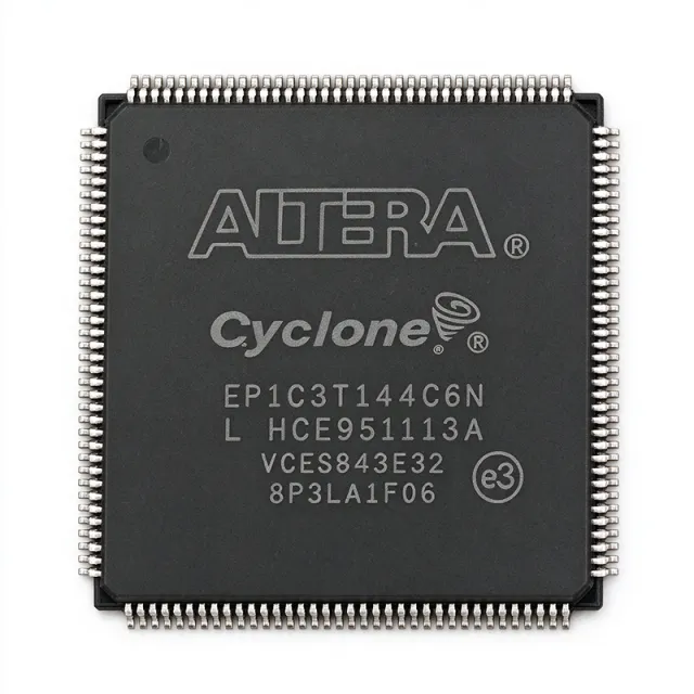
EP1C6F256C8N
EP1C6F256C8N - Cyclone FPGA 6K LE 256-BGA | Intel
The Intel (formerly Altera) EP1C6F256C8N is a Cyclone-series Field-Programmable Gate Array (FPGA) built on a 1.5 V core, 0.13 µm SRAM process, offering 5,980 logic elements (LEs) and 92,160 RAM bits in a 256-ball FineLine BGA (FBGA-256) package. The device is specified for the commercial temperature range (0 °C to +85 °C) and is speed-grade 8. It provides up to 185 user I/O pins and integrates two PLL blocks for clock management, making it a low-cost, high-volume programmable logic option for glue logic, custom interfaces, and parallel processing pipelines.
A Field-Programmable Gate Array (FPGA) is a type of integrated circuit containing an array of configurable logic blocks (CLBs), embedded memory, routing channels, and programmable I/O cells that engineers can re-program in the field after manufacture. Within the broader semiconductor hierarchy, FPGAs sit alongside microcontrollers, DSPs, and ASICs as programmable logic devices, and Cyclone-family parts occupy Intel's low-cost, high-volume tier of that hierarchy. They are widely used to replace discrete glue logic, accelerate parallel data paths, and bridge mismatched interfaces without committing to an ASIC NRE.
Key features of the EP1C6F256C8N include 5,980 LEs, 92,160 bits of embedded RAM (~11.25 KB), 185 user I/Os, two PLLs, and support for LVTTL, LVCMOS, SSTL, and LVDS I/O standards. The Cyclone architecture uses 4-input look-up tables (4-LUTs) per LE and dedicated carry-chain routing for arithmetic, providing predictable timing closure for state machines and DSP-style datapaths up to the device's logic-capacity ceiling.
The device is fabricated on a 1.5 V core, 0.13 µm process, and supports configuration via passive serial (PS), active serial (AS), and JTAG modes. The 256-ball FBGA package has a 17 mm × 17 mm body with a 1.0 mm ball pitch, suitable for multi-layer FR4 PCBs. Each user I/O is organized into banks with per-bank VCCIO rails that can be mixed between 1.5 V, 1.8 V, 2.5 V, and 3.3 V, allowing direct interfacing to memories and processors of different voltage generations on the same board.
Typical applications for this Cyclone device include industrial control and factory automation backplanes, video and image processing pre-processing pipelines, communications protocol bridging (UART, SPI, I2C, parallel bus glue logic), and consumer-electronics display controllers. Designers also use Cyclone FPGAs as low-cost I/O expanders for embedded processors, custom peripheral controllers, and rapid ASIC prototyping.
When designing with the EP1C6F256C8N, observe the I/O-bank VCCIO rules: each bank has its own voltage reference, and mixing 3.3 V LVTTL with 1.5 V SSTL inputs in the same bank is not allowed. Decouple every VCCINT and VCCIO pin with 0.1 µF X7R ceramic capacitors placed as close to the balls as possible, and route the JTAG TCK/TMS/TDO/TDI signals with 4.7 kΩ pull-ups on TCK/TMS to ensure reliable configuration.
This page synthesizes distributor pricing, same-family drop-in speed-grade alternatives, and practical design notes not found in the original Cyclone datasheet, giving procurement and design engineers a consolidated reference for the EP1C6F256C8N.
見積もり
お問い合わせ