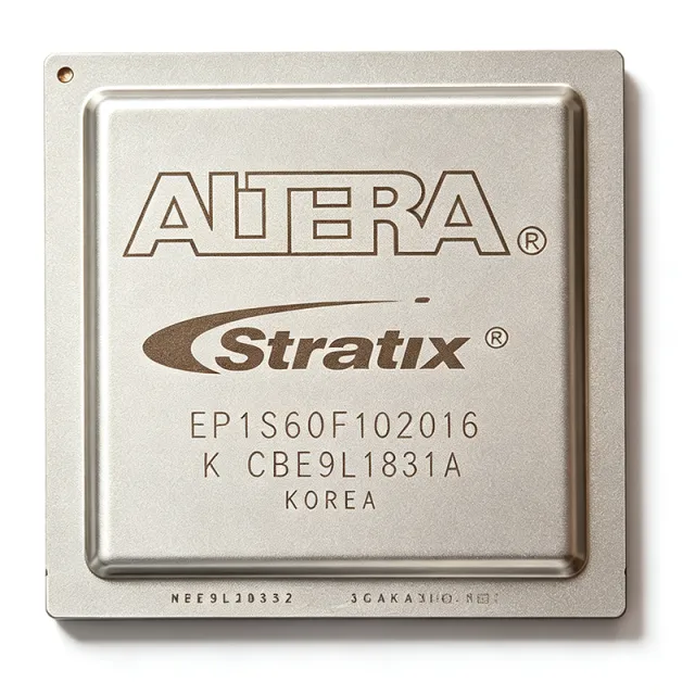
EP1S40F780I6
EP1S40F780I6 - Stratix FPGA 41250 Cells 780-FBGA | Intel
The Intel EP1S40F780I6 is a high-density Stratix family Field Programmable Gate Array (FPGA) built on a 130 nm CMOS process, integrating 41,250 logic elements, 3,423,744 RAM bits, and 615 user I/O pins in a 780-pin flip-chip FineLine BGA package. The industrial-grade "I6" speed grade operates with a core voltage of 1.5 V and supports maximum internal frequencies up to 450.05 MHz.
A Field Programmable Gate Array (FPGA) is a programmable logic device whose architecture comprises an array of configurable logic blocks (CLBs / LABs), programmable routing channels, dedicated DSP blocks, embedded memory blocks, and high-speed transceiver lanes, all controlled by a configuration bitstream loaded at power-up. Within the broader semiconductor hierarchy, an FPGA sits between fixed-function ASICs (lower NRE, higher unit cost at volume) and CPLDs (lower density, non-volatile), offering hardware-level parallelism with re-programmability, making it well-suited to digital signal processing, high-speed interfacing, and prototyping workflows where design iteration is required.
Key features of the EP1S40F780I6 include 4,125 Logic Array Blocks (LABs) supporting up to 41,250 logic elements, dedicated embedded multiplier blocks for DSP arithmetic, embedded TriMatrix memory delivering approximately 3.42 Mbits of on-chip RAM, and a high-performance external memory interface supporting DDR, DDR-II, QDR, and RLDRAM. The device supports configuration via passive serial, passive parallel, fast passive parallel, active serial, and JTAG modes, and integrates on-chip termination (OCT) for clean high-speed signal integrity. Per-device phase-locked loops (PLLs) provide flexible clock synthesis and distribution.
Architecturally, the Stratix family introduced a multi-level interconnect hierarchy and dedicated DSP blocks optimized for high-throughput arithmetic, allowing deterministic timing closure on complex pipelines. The 780-pin FineLine BGA exposes 615 user I/O pins, supporting LVDS, LVPECL, SSTL, HSTL, and other high-speed differential and single-ended I/O standards, with each I/O bank configurable for a dedicated voltage reference.
Typical applications include digital signal processing and baseband prototyping, high-throughput data acquisition front-ends, telecommunications line cards, video and image processing pipelines, military and aerospace signal processing platforms, and ASIC prototyping for SoC verification. The industrial temperature grade extends deployment to factory automation, transportation systems, and outdoor communication equipment.
A key design consideration for the EP1S40F780I6 is multi-rail power sequencing: core (1.5 V), I/O banks (multiple voltages), PLL analog supply, and auxiliary supply must be ramped in the order specified in the device handbook to avoid latch-up. The 780-pin flip-chip BGA also requires a high-layer-count PCB with microvia technology and matched-impedance routing for the DDR memory interface.
This page synthesizes distributor pricing, verified Stratix-family drop-in alternatives from the Site MPN list, and practical design notes not found on individual distributor product pages, providing a consolidated engineering reference for the EP1S40F780I6.
見積もり
お問い合わせ