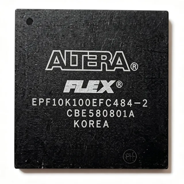
EPF10K100EQC240-1
EPF10K100EQC240-1 - FLEX 10KE FPGA 100K Gates 240-PQFP | Altera
The Altera (now Intel) EPF10K100EQC240-1 is a member of the FLEX 10KE family of SRAM-based FPGAs, integrating 100,000 typical gates, 4,992 logic elements (LEs), and 49,152 bits of embedded RAM in a 240-pin Power Quad Flat Pack (PQFP / BFQFP) package. It provides 189 user I/Os, 624 LABs/CLBs, and is built on a 0.42 µm CMOS process operating from a 2.375 V to 2.625 V core supply with 3.3 V I/O compatibility. The -1 speed grade delivers a propagation delay of approximately 0.4-0.6 ns across the FastTrack interconnect, supporting system clock rates up to 125 MHz in typical designs.
An FPGA (Field Programmable Gate Array) is a semiconductor integrated circuit whose logic function is defined after manufacturing by a configuration bitstream loaded into SRAM cells. Within the broader taxonomy, FPGAs sit beside CPLDs (Complex Programmable Logic Devices) inside the PLD (Programmable Logic Device) family, and represent the highest-density, highest-performance tier of general-purpose programmable logic. FPGAs are commonly used to implement glue logic, custom datapaths, bus interfaces, and prototype ASICs before tape-out. The FLEX 10KE family specifically introduced embedded array blocks (EABs) for on-chip RAM and ROM, enabling System-on-a-Programmable-Chip (SOPC) integration.
Key features include embedded array blocks (EABs) for synchronous RAM and ROM, multi-level FastTrack interconnect routing, JTAG (IEEE 1149.1) boundary-scan test support, and built-in PCI compliance. The architecture combines 4,992 LEs distributed across 624 LABs with 12 embedded array blocks of 2,048 bits each, totaling 24 Kbits of dedicated memory expandable to 49 Kbits when using LE-based RAM. MultiVolt I/O pins support 3.3 V, 2.5 V, and 1.8 V interfaces through dedicated VCCIO banks, simplifying mixed-voltage design.
The FLEX 10KE architecture separates logic and interconnect resources into rows and columns, with each Logic Array Block containing 8 LEs, a carry chain, and a cascade chain for arithmetic and wide fan-in functions. The embedded array blocks serve as 2,048-bit memory blocks configurable as RAM, ROM, or lookup tables. Configuration data is loaded serially via a 5-pin interface or via the ByteBlaster/parallel port cable, supporting in-system programmability. Operating temperature range is 0 °C to 70 °C for the commercial grade, with the device consuming low standby current typical of SRAM-based FPGAs.
Typical applications include telecommunications line cards, industrial control glue logic, PCI bus bridges, peripheral controllers, and legacy system upgrades where migration from discrete TTL or older PLDs is required. The 189 user I/Os make the EPF10K100E well-suited to bus-intensive designs with multiple external interfaces.
When designing with this device, verify that the I/O bank voltages match those of connected peripherals, since 5 V tolerance is not provided on all pins. The 240-pin PQFP package requires careful PCB layout with adequate power and ground planes, and the -1 speed grade should be derated appropriately when calculating setup and hold margins for high-speed synchronous interfaces.
This page synthesizes distributor pricing, drop-in alternatives from the FLEX 10KE family, and practical design notes not found in the original manufacturer datasheet alone.
見積もり
お問い合わせ