EPM1270F256
EPM1270F256 - MAX II 980-Macrocell CPLD, 256-BGA | Altera
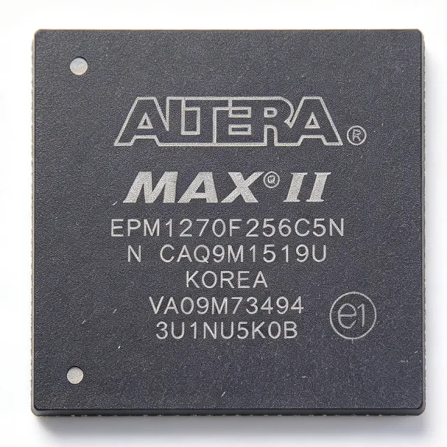
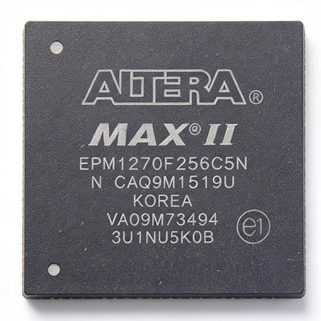
The Altera (Intel PSG) EPM1270F256 is a member of the MAX II family of instant-on, non-volatile CPLDs, offering 980 typical equivalent macrocells (1270 LEs) in a 256-pin FineLine BGA package. According to the manufacturer datasheet, the device is built on a 0.18 µm process, operates from a 2.5 V / 3.3 V core supply, and supports user I/O up to 212 pins with a system frequency up to 201.1 MHz. It uses a non-volatile flash configuration cell that delivers instant-on functionality and eliminates external boot memory, simplifying board design in glue-logic and bus-interface applications.
A CPLD (Complex Programmable Logic Device) is a non-volatile programmable logic device that combines the architectural simplicity, deterministic timing, and instant-on behavior of classic PAL/GAL logic with modern high-pin-count integration. Within the broader programmable-logic taxonomy, the MAX II family sits between simple 5-V SPLDs and high-density SRAM-based FPGAs: like SPLDs it is non-volatile and pin-configurable, but like an FPGA it integrates thousands of gates and dozens of I/O standards. MAX II devices are widely used as interface bridges, I/O expanders, and timing controllers in cost-sensitive industrial and consumer systems.
Key features of the EPM1270F256 include 980 macrocells / 1270 logic elements, 8 Kbits of user flash memory, on-chip voltage regulators supporting 3.3 V, 2.5 V, 1.8 V, and 1.5 V operation, MultiVolt core and I/O supporting mixed-voltage interfacing, JTAG (IEEE 1149.1) boundary-scan programming, and an instant-on configuration time measured in microseconds. The 256-pin FineLine BGA footprint provides flexible I/O bank placement while preserving vertical migration to the EPM570 and EPM2210 in the same package.
Architecturally, the EPM1270F256 implements the Logic Array Block (LAB) structure with 16 macrocells per LAB, a fast t<sub>PD</sub> in the single-digit nanosecond range, and a deterministic interconnect that makes it well-suited for I/O glue, address decoding, register insertion, and state-machine implementation. The non-volatile flash cell removes the need for a separate configuration PROM, lowering BOM cost and enabling secure in-system updates via JTAG.
Typical applications include bus-interface bridging (e.g., PCI to local bus), I/O expansion and voltage translation, power-up sequencing logic, motor-control and industrial automation glue, LED display driving and refresh, and consumer-electronics control logic where instant-on behavior and low unit cost matter more than raw logic density.
When designing with the EPM1270F256, ensure that the chosen I/O standard matches the bank's VCCIO supply and respect the device's MultiVolt I/O rules when bridging 1.5 V, 1.8 V, 2.5 V, and 3.3 V domains. Decoupling must follow the Quartus II power-pin guidance; leaving the on-chip regulator's decoupling incomplete can cause VCCINT ripple that degrades t<sub>PD</sub> margins.
This page synthesizes distributor pricing, drop-in alternatives in the same 256-pin FineLine BGA footprint, and practical design notes drawn from the MAX II handbook to give engineers a single decision-ready view not found in the bare datasheet.
USD $10.85
お問い合わせ