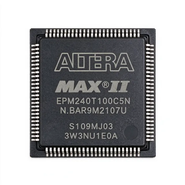
EPM240T100I3N
EPM240T100I3N - 192-Macrocell MAX II CPLD, 100-TQFP, Industrial | Intel
The Intel (Altera) EPM240T100I3N is a non-volatile MAX II family Complex Programmable Logic Device (CPLD) delivering 192 macrocells, 80 user I/O pins, and 8 Kbits of on-chip flash configuration memory in a 100-pin TQFP (T100) package. The 'I' speed/temperature grade designation indicates the industrial -40C to +100C junction operating range with a 304 MHz internal performance figure, fabricated on a 0.18 um six-layer-metal flash process and supported by 2.5 V/3.3 V core and I/O supply rails. This is the MAX II instant-on, low-power variant in legacy Altera packaging with vertical migration to the EPM570 and EPM1270 in the same footprint.
A CPLD (Complex Programmable Logic Device) is a non-volatile programmable logic IC that sits between simple SPLDs/GLUE-logic PALs and high-density FPGAs in the programmable logic hierarchy. CPLD -> programmable logic -> PLD -> digital logic -> semiconductor. MAX II devices use a flash-based configuration cell instead of an external configuration ROM, giving them instant-on behavior (sub-millisecond wake-up), deterministic timing (no boot loader), and excellent suitability for I/O expansion, bus bridging, power-sequencing glue logic, and state-machine control. Compared to FPGAs, CPLDs such as the EPM240 offer lower static power, fixed propagation delay, and unlimited in-system reprogrammability via JTAG.
Key features of the EPM240T100I3N include 192 macrocells distributed across 4 logic array blocks (LABs), 80 maximum user I/O, 4.6 ns pin-to-pin logic delay, a JTAG/IEEE 1149.1 compliant interface for in-system programmability (ISP), MultiVolt I/O supporting 1.5 V, 1.8 V, 2.5 V, and 3.3 V interfaces, and an internal oscillator usable for simple clocking. The on-chip User Flash Memory block (8 Kbits) can store constants, serial numbers, or board revision IDs without an external EEPROM.
Architecturally, the MAX II family uses a continuous, non-segmented flash memory cell per macrocell. Combined with a fine-grained logic element and a global LAB interconnect, this yields predictable 4.6 ns tPD1 propagation delay regardless of how many macrocells are used, simplifying static timing closure. The 100-pin TQFP package uses a standard JEDEC 14x14 mm body, 0.5 mm pitch, MSL-3 moisture sensitivity, and a -40C to +100C industrial junction temperature rating.
Typical applications include I/O expansion and voltage-level translation in industrial controllers, glue-logic integration on FPGA-based motherboards, power-sequencer and watchdog controllers, JTAG-controlled bus bridges (I2C/SPI to parallel), LED-driver state machines, and motor-control peripheral interfaces. The instant-on, non-volatile nature of the EPM240 is especially valuable in safety-critical or deterministic-latency designs where FPGAs cannot meet cold-boot timing.
Designers should note that the EPM240T100I3N is being phased out as part of the MAX II EOL roadmap; new designs should consider the MAX V family (5M80ZE64, 5M160ZE64) or MAX 10 (10M02) family for long-term availability. The Quartus II / Quartus Prime design software with MAX II device support remains available from Intel. This page synthesizes distributor pricing, same-brand drop-in alternatives (EPM240T100C5N, EPM240T100C4N, EPM240GT100I5N, EPM240GT100C5N, EPM240GT100C4N), and design notes not found in the manufacturer datasheet.
見積もり
お問い合わせ