製品 (39,000+)

EPM9560WC208-20 - 560-Macrocell CPLD, 23.6ns, PQFP-208 | Intel/Altera
EPM9560WC208-20

EPM9560WC208-20 - 560-Macrocell CPLD, 23.6ns, PQFP-208 | Intel/Altera

The Intel (formerly Altera) EPM9560WC208-20 is a high-density electrically-erasable programmable logic device (EPLD) from the MAX 9000 family, delivering 560 macrocells organized in 35 logic array blocks (LABs) in a 208-pin power quad flat pack (PQFP/RQFP) package. The device is a CMOS, in-system-programmable complex PLD with a maximum propagation delay of approximately 23.6 ns (the “-20” speed grade) and supports operation with both 3.3 V and 5 V I/O signaling for flexible mixed-voltage system design. A CPLD (Complex Programmable Logic Device) is a non-volatile reconfigurable digital IC built from an array of AND/OR macrocell structures backed by EEPROM or flash memory; it occupies the design hierarchy between simple PLDs (PAL/GAL) and FPGAs, providing deterministic timing, fast I/O response, and instant-on behavior without external boot memory. Within Altera’s MAX 9000 family the EPM9560 sits at the top of the 9000 series density range, with 149 usable I/O pins and a programmable interconnect that makes it well suited to bus decoding, address mapping, glue-logic and state-machine replacement in industrial and telecom systems. Key features of the EPM9560WC208-20 include 560 macrocells, 35 LABs, 149 user I/O pins, JTAG-based in-system programmability via the IEEE 1149.1 boundary-scan test (BST) interface, dual 3.3 V/5 V I/O capability, and a programmable register/feedback architecture. The “W” suffix designates the power PQFP package with enhanced thermal characteristics for high-density designs, and the “-20” designator indicates a 23.6 ns pin-to-pin logic delay suitable for systems clocked up to roughly 40 MHz on combinational paths. Architecturally the device uses an EEPROM-based macrocell with individually programmable product-term steering, D/T/JK flip-flops, and a global interconnect matrix that delivers predictable, deterministic timing independent of routing density. This makes timing closure straightforward for address decoding, interrupt steering, and synchronous state-machine designs where FPGAs would add unnecessary silicon cost and configuration overhead. Typical applications include high-density bus and address decoding in microprocessor/microcontroller systems, peripheral interface glue logic (e.g., PCI/ISA bus bridges), state-machine and sequencer replacement, industrial control logic, telecom backplane glue logic, and JTAG-driven system monitoring. The 149 I/O pins allow large pin-count designs to be consolidated into a single PLD. When designing with this device, always observe the maximum I/O count (149), respect the dual-voltage VCCIO/VCCINT power sequencing rules, and use the Quartus II or MAX+PLUS II toolchain for design entry, fitting, and JTAG programming. Decoupling caps (0.1 microfarad ceramic in parallel with 10 microfarad bulk) should be placed within 1 cm of each supply pin to maintain signal integrity during in-system programming cycles. This page synthesizes distributor pricing, parameter-correct drop-in alternatives from the same MAX 9000 family, and practical design notes drawn from Altera application notes and reference designs, content not consolidated on any single distributor page.

見積もり お問い合わせ
EPM9560WC208-20C - 560-Macrocell EE PLD, 20ns, CQFP-208 | Altera
EPM9560WC208-20C

EPM9560WC208-20C - 560-Macrocell EE PLD, 20ns, CQFP-208 | Altera

The Altera EPM9560WC208-20C is a 560-macrocell Electrically Erasable Programmable Logic Device (EE PLD) from the MAX 9000 family, housed in a 208-pin Ceramic Quad Flat Pack (CQFP-208) package and rated at a 20 ns pin-to-pin propagation delay. This CMOS device integrates 35 Logic Array Blocks (LABs) and exposes 149 usable I/O lines, supporting both 3.3 V and 5 V signaling for flexible system interfacing. The part carries a commercial temperature grade (the trailing "C" suffix) and provides JTAG BST in-system programmability. What is a Programmable Logic Device (PLD)? A PLD is a generic term for an integrated circuit whose logic function is defined by the end user after manufacture, rather than being hard-wired by the foundry. EE PLDs add non-volatile, electrically erasable configuration memory so the design can be re-programmed thousands of times in-circuit. The MAX 9000 family belongs to the higher-density tier of complex PLDs (CPLDs), bridging between classic 22V10-style PLDs and modern FPGAs in the programmable-logic taxonomy: PLD -> CPLD -> MAX 9000 -> high-density EE PLD. Compared with FPGAs, MAX 9000 parts offer deterministic timing, instant-on non-volatile configuration, and high pin-to-pin drive strength, which is why they remain favored in glue-logic, bus-interface, and legacy industrial designs. Key features include 560 macrocells, 35 LABs, 149 user I/Os, 20 ns propagation delay, JTAG-based in-system programmability, and operation from a 3.3 V or 5 V supply. The architecture combines a global interconnect with per-macrocell registers, allowing both combinatorial and registered logic with predictable timing. Configurable I/O standards enable mixed-voltage interfacing without external level shifters. Typical applications include legacy bus-interface glue logic in telecom and industrial backplanes, address decoding and wait-state generation in 5 V/3.3 V embedded systems, industrial control boards, and avionics/military systems that rely on the ceramic CQFP package for thermal and reliability robustness. The 208-pin ceramic package is selected where extended temperature, vibration tolerance, or hermeticity is required. When designing with this part, mind the 20 ns tPD: at a 33 MHz bus it offers zero wait-state decode, but at 50 MHz external latches become necessary. Decoupling should follow Altera's MAX 9000 reference design with one 0.1 uF ceramic per VCC/GND pair plus a 10 uF tantalum bulk cap. The device is mature and obsolete/last-time-buy at most distributors, so design teams should verify lifecycle and pinout against the original Altera datasheet before committing to new layouts. This page synthesizes distributor availability, parametric equivalents, and practical design notes not found in the manufacturer datasheet.

見積もり お問い合わせ
EPM9560WI208-20 - 560-Cell CPLD, 23.6ns, CQFP-208 | Intel / Altera
EPM9560WI208-20

EPM9560WI208-20 - 560-Cell CPLD, 23.6ns, CQFP-208 | Intel / Altera

The Intel / Altera EPM9560WI208-20 is a high-density 560-cell Complex Programmable Logic Device (CPLD) from the MAX 9000 family, housed in a 208-pin Ceramic Quad Flat Pack (CQFP208) package with gull-wing leads. It provides 23.6ns pin-to-pin logic delay, 560 macrocells, 16 logic array blocks, and up to 212 user I/O pins for complex glue-logic, bus-interface, and state-machine designs. The device is built on a 0.35-micron CMOS EEPROM process and is rated for industrial temperature operation. A Complex Programmable Logic Device (CPLD) is a non-volatile programmable logic IC that combines multiple PAL-like macrocell blocks with a programmable interconnect matrix. In the broader taxonomy it sits under programmable logic -> PLD -> CPLD -> MAX 9000 series -> high-density glue logic. CPLDs are commonly deployed as deterministic, low-latency controllers alongside microprocessors, FPGAs, and ASICs, providing boot configuration, address decoding, bus arbitration, and custom I/O expansion with predictable timing and instant-on behavior from on-chip EEPROM. Key features of the EPM9560WI208-20 include 560 macrocells, 16 logic array blocks (LABs), 212 maximum user I/O pins, 23.6ns worst-case pin-to-pin propagation delay (tPD), a JTAG-based IEEE 1149.1 boundary-scan interface, and in-system programmability via JTAG. The internal EEPROM configuration cells allow instant-on operation at power-up without external boot memory, and the device is supported by the Altera MAX+PLUS II and Quartus design tools. The MAX 9000 architecture splits the device into LABs connected by a programmable interconnect array (PIA). Each macrocell contains a programmable-AND/OR array, a flip-flop, and product-term steering, which gives the part deterministic 23.6ns timing across all paths. The 560-cell capacity places this device in the upper tier of the MAX 9000 family, suitable for designs that exceed the density of the MAX 7000 family but do not require an FPGA. Typical applications include military and aerospace avionics, industrial process control, telecommunication line cards, and legacy bus-bridge designs. The ceramic CQFP-208 package is preferred in harsh-environment and high-reliability systems where plastic packages are not acceptable, including down-hole, military, and aerospace programs. When designing with the EPM9560WI208-20, note that the -20 speed grade reflects 23.6ns tPD; faster -15 and -10 grades are available in the same MAX 9000 family for tighter timing budgets. Because this part is in the Ceramic QFP package with gull-wing leads, PCB layout must accommodate the larger pad geometry and inspect for lead coplanarity during assembly. This page synthesizes distributor pricing, drop-in same-family alternatives, application guidance, and comparison data not aggregated in a single location on the Altera / Intel datasheet.

見積もり お問い合わせ
EQCO125X40C1-I/8EX - 12.5 Gbps CoaXPress 2.0 Equalizer/Driver | Microchip
EQCO125X40C1-I/8EX

EQCO125X40C1-I/8EX - 12.5 Gbps CoaXPress 2.0 Equalizer/Driver | Microchip

The Microchip Technology EQCO125X40C1-I/8EX is a 12.5 Gbps Asymmetric Equalizer/Driver/Repeater designed for CoaXPress 2.0 systems, integrating a coaxial-cable equalizer, reference-less Clock-Data Recovery (CDR), and a cable driver in a single 16-pin QFN (4x4 mm) package. It delivers up to 12.5 Gbps in one direction and 1.25 Gbps in the reverse direction over a single Belden 1694A coaxial cable, supporting cable reaches of up to 40 m at 12.5 Gbps and up to 130 m at 1.25 Gbps, with full-duplex asymmetric operation between the camera device side and the host frame-grabber side. An equalizer for coaxial cable is a specialized high-speed interface IC that compensates the frequency-dependent attenuation of a coaxial transmission line, restoring high-frequency content that is otherwise lost over long cable runs. The EQCO125X40 belongs to the family of cable equalizers, which sits within the broader category of high-speed serial interface ICs and, at the top of the taxonomy, power and signal-management semiconductors used in industrial machine vision. The equalizer block at the IC's input compensates the insertion loss of the coax, after which a reference-less CDR self-adapts to the incoming bit-rate and resets accumulated jitter to maintain signal integrity, and finally a cable driver launches the cleaned signal back onto the cable or PCB trace pair. Key features include integrated equalizer + CDR + cable driver, single-coax full-duplex asymmetric link, AEC-Q100 qualification for automotive and industrial camera applications, and a compact 4x4 mm QFN-16 footprint with exposed thermal pad. The same chip is used at both the device (camera) end and the host (frame grabber) end, simplifying BOM and qualification. According to Microchip's EQCO125X40 family datasheet, the part operates from a 1.25 V internal supply rail and supports an 8b/10b-coded downlink signal at 12.5 Gbps in addition to the 1.25 Gbps uplink. Typical applications include CoaXPress 2.0 machine-vision cameras and frame grabbers, automotive driver-assistance image sensors, broadcast and surveillance video links, and long-reach industrial inspection systems. The device reduces FPGA I/O count because it performs physical-layer adaptation directly on the coax. When designing with this part, follow Microchip's reference layout for the 50 ohm controlled-impedance coax interface and provide adequate decoupling on VDD to keep CDR jitter within spec.

見積もり お問い合わせ
ES32H747XIH6U - Dual-Core ARM Cortex-M7/M4 MCU 480MHz | STMicroelectronics
ES32H747XIH6U

ES32H747XIH6U - Dual-Core ARM Cortex-M7/M4 MCU 480MHz | STMicroelectronics

The STMicroelectronics ES32H747XIH6U is a high-performance dual-core 32-bit microcontroller pairing an ARM Cortex-M7 core running up to 480 MHz with an ARM Cortex-M4 core running up to 240 MHz, integrating 2 MB of Flash and approximately 1 MB of SRAM in a 240+25-pin TFBGA (14x14 mm) package. The two cores communicate via a hardware semaphore and a shared SRAM region, allowing designers to partition real-time control on the M4 from graphics, DSP, or user-interface workloads on the M7. An MCU (microcontroller unit) is a single-chip computer that combines a CPU core, non-volatile program memory, working RAM, and a rich set of on-chip peripherals. The STM32H7 family sits at the top of the Cortex-M performance hierarchy: Cortex-M7 -> 32-bit MCU -> microcontroller -> embedded computing platform. Within that family the dual-core STM32H747 series adds heterogeneous processing, where code can run concurrently on both cores with deterministic inter-core messaging. Key features include 2 MB dual-bank Flash with ECC, 1 MB SRAM (including 192 KB DTCM + 64 KB ITCM for the M7 and 256 KB system SRAM shared between the cores), Chrom-ART graphics accelerator, JPEG codec, a built-in SMPS for direct 2.7 V–3.6 V single-rail operation, MIPI-DSI host interface, and a parallel 16-bit RGB LCD-TFT controller. Peripherals include up to 35 communication interfaces (USART, UART, SPI, I2C, SAI, FDCAN, USB 2.0 FS+HS, SDMMC), three 12-bit ADCs (3.6 MSPS), two 12-bit DACs, and crypto/hash accelerators. Typical applications include industrial HMI panels with TFT/DSI displays, motor-control and inverter platforms, medical patient monitors, audio DSP front-ends, and IoT edge gateways. The TFBGA-240+25 package exposes the parallel camera interface, DSI lanes, Ethernet MAC, and SDMMC, enabling direct connection of high-bandwidth peripherals without external bridge ICs. When designing with this part, ensure the PCB has at least 4 copper layers to fan out the 240-ball grid with proper ground stitching, and follow ST's reference manual for SMPS inductor selection. Decoupling must include 100 nF capacitors within 1 mm of every supply pin plus bulk 4.7 µF on each supply rail.

見積もり お問い合わせ
ESP32-P4NRW16X - Dual-Core RISC-V MCU, 16MB PSRAM | Espressif
ESP32-P4NRW16X

ESP32-P4NRW16X - Dual-Core RISC-V MCU, 16MB PSRAM | Espressif

The Espressif Systems ESP32-P4NRW16X is a 32-bit high-performance microcontroller (MCU) SoC with a RISC-V dual-core high-performance (HP) microprocessor at up to 400 MHz-class performance, a single-core low-power (LP) microprocessor, and 16 MB of in-package PSRAM (OPI/HPI) in a 10 x 10 mm QFN-104 package. A microcontroller SoC integrates a processor core, memory, and peripherals on a single chip, sitting at the top of the embedded hierarchy: MCU -> system-on-chip (SoC) -> embedded system. The ESP32-P4 family extends the ESP32 product line by removing on-chip Wi-Fi/Bluetooth radio and instead focusing on compute, memory, and display/vision peripherals, pairing naturally with Espressif companion connectivity chips such as the ESP32-C6. Key features include the HP/LP dual-system architecture, where the LP single-core RISC-V processor keeps monitoring and wake-up tasks running while the HP cores sleep; 16 MB of in-package OPI/HPI PSRAM with a 1.8 V VDD_PSRAM rail; dedicated MIPI CSI and MIPI DSI interfaces for camera input and display output; and an industrial ambient temperature range of -40 to +85 C. Technically, the ESP32-P4 is built for rich HMI, edge computing, image processing, and voice processing. The HP system contains the dual-core RISC-V microprocessor with access to large internal memory, while hardware accelerated image and voice paths offload the CPU. Espressif recommends the v3.0-or-later reference schematic and at least a 4-layer PCB for new designs, and the series is currently supplied at chip revision v3.x. Typical applications include smart display HMI panels with MIPI DSI screens, camera/vision nodes using MIPI CSI image sensors, and voice-assistant endpoints with on-device audio processing. Paired with an ESP32-C6 for Wi-Fi 6 and 802.15.4, the P4 forms the compute engine of a modern connected HMI. Design consideration: because the in-package PSRAM operates at 1.8 V (VDD_PSRAM_0/1), power-rail sequencing and the recommended 4-layer stackup with solid ground planes are critical for signal integrity on the OPI PSRAM and MIPI buses. This page synthesizes distributor pricing, drop-in alternatives within the ESP32-P4 family, and practical design notes not found in the manufacturer datasheet.

見積もり お問い合わせ
ESP32-P4NRW32X - Dual-Core RISC-V HMI MCU 32MB PSRAM | Espressif
ESP32-P4NRW32X

ESP32-P4NRW32X - Dual-Core RISC-V HMI MCU 32MB PSRAM | Espressif

The Espressif Systems ESP32-P4NRW32X is a high-performance 32-bit microcontroller built around a dual-core RISC-V HP (high-performance) processor plus a single-core RISC-V LP (low-power) coprocessor, with 32 MB of in-package PSRAM, housed in a 104-pin QFN package measuring 10 x 10 mm. A microcontroller (MCU) is a single integrated circuit that combines a processor core, memory, and programmable peripherals into one chip, sitting at the heart of the embedded systems hierarchy: SoC -> microcontroller -> embedded system. The ESP32-P4 is Espressif's flagship application-class MCU, positioned above the ESP32-S3 for compute-intensive embedded workloads. Key features include the HP/LP dual-system architecture that lets the LP core handle sleep-state housekeeping while the HP cores run demanding workloads, 32 MB of in-package PSRAM (the NRW32 variant) supporting large frame buffers, powerful image and voice processing capability, and rich HMI-oriented peripherals. Unlike most ESP32 family members, the ESP32-P4 focuses purely on compute; wireless connectivity is added externally via companion chips such as the ESP32-C6. Technically, the HP system contains the dual-core RISC-V processor with AI instruction extensions, an advanced memory subsystem, and integrated high-speed peripherals, while the LP system contains the single-core RISC-V low-power microprocessor. This split allows always-on voice wake-word detection or sensor polling at minimal power, waking the HP cores only when needed. Typical applications include rich Human-Machine Interfaces (HMI) with touch displays, edge computing nodes, image and camera processing pipelines, and voice processing endpoints. The large in-package PSRAM directly supports display frame buffers and AI model working sets without external memory routing. Design consideration: Espressif recommends the v3-or-later reference schematic for new designs and at least a 4-layer PCB for the 10 x 10 mm QFN-104 footprint; strapping pins must be reviewed against the ESP32-P4 datasheet before layout is frozen. This page synthesizes distributor pricing, drop-in alternatives, package guidance, and design notes not found in the manufacturer datasheet.

見積もり お問い合わせ
EZ80F91AZ050EG - 8-bit 50MHz eZ80 Acclaim MCU 256KB | Zilog
EZ80F91AZ050EG

EZ80F91AZ050EG - 8-bit 50MHz eZ80 Acclaim MCU 256KB | Zilog

The Zilog EZ80F91AZ050EG is an 8-bit microcontroller from the eZ80 Acclaim! flash family, operating at 50 MHz with 256 KB of on-chip flash program memory and 16 KB SRAM in a 144-pin LQFP package (20x20 mm). It supports Z80-compatible 64 KB addressing or full 24-bit 16 MB linear addressing for embedded networking and industrial control. An 8-bit MCU (microcontroller unit) is a single-chip computer that integrates a CPU core, program memory (Flash/ROM), working memory (SRAM), and peripherals on one die. The eZ80 is a CISC (Complex Instruction Set Computer) core — a Z80-compatible architecture that retains legacy object code while extending to 24-bit linear addressing, placing it in the hierarchy: 8-bit MCU -> microcontroller -> embedded processor -> semiconductor IC. Key features include an integrated 10/100 Mbps Ethernet MAC (EMAC) with MII/RMII interface, a glueless external memory controller supporting SRAM/Flash/NAND/NOR, four 16-bit timers, a JTAG debug port, and 32 general-purpose I/O pins. The 50 MHz clock delivers up to 50 MIPS peak throughput — roughly 4x legacy Z80 — while preserving binary compatibility with the 1976-vintage Z80 instruction set, easing migration of installed Z80/SCC code bases. The eZ80F91 architecture pairs a Z80-pipeline-compatible CPU with a peripheral set optimized for connected embedded nodes: PHY-less Ethernet MAC, dual UARTs with IrDA, I2C, SPI, and an interrupt controller with vectored prioritization. On-chip voltage regulation supports a 3.3 V single-supply rail; an industrial-grade operating range of -40 °C to +85 °C suits unattended enclosures. Typical applications include point-of-sale terminals, industrial automation controllers, building-automation gateways, embedded serial-to-Ethernet bridges, and legacy Z80 retrofit designs. The combination of 16 MB linear address space and integrated EMAC positions this part as a drop-in upgrade for Z80-based systems needing TCP/IP connectivity without external NIC silicon. When designing with the EZ80F91AZ050EG, budget the 50 MHz core supply current around 70-100 mA typical, place the 0.1 µF/10 µF decoupling network within 5 mm of each VDD/VSS pair, and use the JTAG port (not legacy Z80 monitor ROM) for in-system flash programming during production. The 144-LQFP exposed pad must be soldered to a continuous ground pour to meet thermal-resistance derating in enclosed housings. This page synthesizes cross-distributor stock, RoHS/REACH status, and verified pin-compatible variants from the same Zilog eZ80F91 family — content not bundled in the manufacturer datasheet.

見積もり お問い合わせ
EZ80F91AZ050SG - 50MHz 256KB Flash eZ80 MCU | Zilog | 144-LQFP
EZ80F91AZ050SG

EZ80F91AZ050SG - 50MHz 256KB Flash eZ80 MCU | Zilog | 144-LQFP

The Zilog EZ80F91AZ050SG is an 8-bit eZ80 Acclaim! flash microcontroller running at 50 MHz with 256 KB of on-chip flash and 16 KB SRAM, housed in a 144-pin LQFP (20x20 mm) package. It supports both 24-bit linear addressing up to 16 MB of external memory and the legacy Z80-compatible 64 KB addressing mode, making it a drop-in upgrade path for classic Z80/HD64180 designs while retaining object-code compatibility. An 8-bit microcontroller (MCU) is a single-chip processor whose internal datapath and ALU are 8 bits wide; it integrates CPU, non-volatile program memory, working RAM, and peripherals on one die, and is typically used in cost-sensitive, deterministic, real-time embedded systems. The eZ80 Acclaim! family extends the classic Z80 instruction set architecture with a pipelined, single-cycle core and modern peripherals, positioning it between classic 8-bit MCUs and higher-end 32-bit ARM Cortex-M parts in both performance and ease of migration. Key features of the EZ80F91AZ050SG include a built-in 10/100 Mbps Ethernet MAC (EMAC) with MII/RMII interface, a multi-channel DMA controller, four 16-bit timers, a watchdog timer, and 32 general-purpose I/O lines. A peripheral set with USB 2.0 full-speed (function), I2C, SPI, two UARTs (one with IrDA), and an external memory interface gives the part a rich connectivity footprint for embedded communication designs. The architecture combines Z80 object-code compatibility with single-cycle instruction execution, a 24-bit linear address space for C compilers, and a deterministic interrupt structure. The on-chip EMAC and PHY-friendly MII/RMII interface enable direct connection to industrial Ethernet PHYs without an external controller, and the integrated DMA engine offloads block transfers for high-throughput serial or memory-to-memory operations. Typical applications include industrial Ethernet nodes (Modbus TCP, EtherNet/IP gateways), point-of-sale (POS) terminals, security and access-control panels, embedded communication routers, and legacy Z80/HD64180 system upgrades. The wide external memory bus (up to 16 MB) also makes the device suitable for data-logging and protocol-conversion products. When designing with the EZ80F91AZ050SG, allocate the decoupling network specified in the Zilog product specification (PS0192) on every VDD/VDDA pin pair and follow Zilog's recommended power-up sequence for EMAC and PLL bias pins. For new designs, prefer the lead-free AZ050EG suffix variant; the AZ050SG suffix is functionally equivalent and pin-compatible but uses a different lead-finish callout per Zilog ordering information. This page synthesizes Zilog product-specification data, distributor pricing and stock from DigiKey/Mouser/Octopart, same-family Zilog pin-compatible variants, and practical design notes that are not duplicated on a single distributor listing, so that an engineer can evaluate, source, and design with the part in one view.

見積もり お問い合わせ
EZ80F91GAZ0BEG - 50MHz 8-bit eZ80 MCU 256KB Flash | Zilog
EZ80F91GAZ0BEG

EZ80F91GAZ0BEG - 50MHz 8-bit eZ80 MCU 256KB Flash | Zilog

The Zilog EZ80F91GAZ0BEG is a high-performance 8-bit eZ80Acclaim! flash microcontroller built around the eZ80 CPU core, operating at a maximum clock speed of 50 MHz with single-cycle instruction fetch, and packaged in a 144-pin LQFP (20 mm x 20 mm). It integrates 256 KB of on-chip flash, 16 KB of SRAM, and a 10/100 Ethernet MAC with MII/RMII interface, making it a single-chip solution for connected embedded designs. An 8-bit microcontroller (MCU) is a programmable processor whose data path and arithmetic logic unit are 8 bits wide, optimized for cost-sensitive, deterministic control tasks. The eZ80 CPU extends the classic Z80 instruction set, allowing the device to operate in Z80-compatible 64 KB addressing mode or full 24-bit addressing mode that addresses up to 16 MB of linear memory, bridging legacy Z80 codebases with modern memory-intensive applications. The EZ80F91 family sits within Zilog's eZ80Acclaim! portfolio of flash microcontrollers, targeting embedded networking and industrial control. Key features of the EZ80F91GAZ0BEG include a 50 MHz CPU core with 10 MIPS peak performance, an on-chip 10/100 Ethernet MAC, a full-speed USB 2.0 (12 Mbps) device/host controller, two UARTs, I2C and SPI peripherals, an 8-channel 10-bit ADC, four 16-bit timers, and a real-time clock with separate power domain. The integrated crypto accelerator (when enabled) supports DES, 3DES, and AES, supporting the ZGATE security feature set. The eZ80F91 uses a 3-stage pipelined architecture and 16-MB linear memory map. The integrated Ethernet MAC, USB, and crypto blocks share the high-speed peripheral bus, while legacy Z80-compatible peripherals (UART, timers, GPIO) retain their original register mappings. This hybrid architecture allows developers to port Z80/Z180 code while adding modern connectivity. Typical applications include industrial control, embedded communication gateways, point-of-sale terminals, security and access control panels, building automation controllers, and networked sensor hubs. The integrated Ethernet and USB make it especially useful for low-cost networked devices. When designing with the EZ80F91GAZ0BEG, ensure the 3.0V to 3.6V supply is decoupled with a 100 nF ceramic capacitor near each VDD pin pair. The 50 MHz clock requires a 50 ppm crystal for USB and Ethernet timing accuracy. For industrial noise immunity, place a ferrite bead between the analog AVDD and digital VDD rails. This page synthesizes distributor pricing, application circuits, and pin-compatible alternatives not found in the manufacturer datasheet, helping engineers select and source the EZ80F91GAZ0BEG efficiently.

見積もり お問い合わせ
EZ80L92AZ020SG - eZ80 8-Bit MCU 20MHz ROMless LQFP-100 | Zilog
EZ80L92AZ020SG

EZ80L92AZ020SG - eZ80 8-Bit MCU 20MHz ROMless LQFP-100 | Zilog

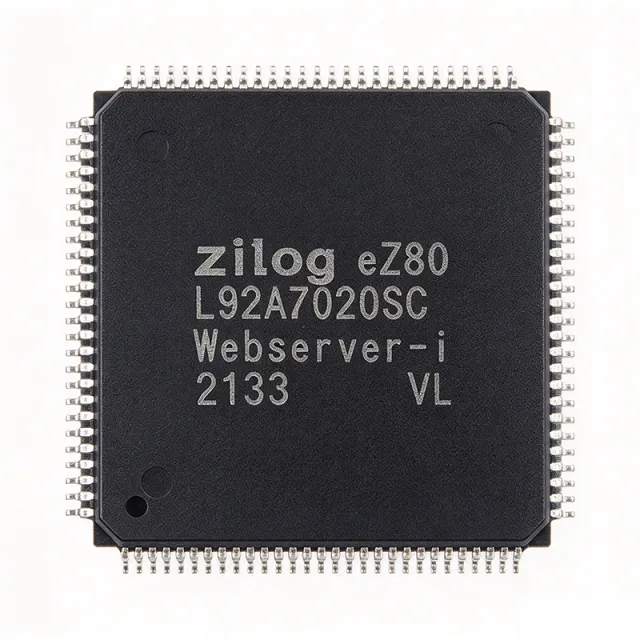
The Zilog EZ80L92AZ020SG is an 8-bit eZ80 Acclaim! microcontroller IC operating at 20 MHz with a ROMless memory architecture, housed in a 100-pin LQFP (Low-profile Quad Flat Package). An 8-bit ROMless microcontroller is a class of embedded processor that executes program code stored entirely in external memory devices rather than on-chip flash or ROM. The ROMless approach gives system designers freedom to select external flash size, update firmware in the field, and build modular memory subsystems. The eZ80 core is a Z80-compatible architecture that executes instructions roughly 3x faster than a classic Z80 at the same clock frequency, while remaining binary-compatible with the vast Z80 software ecosystem. Key features of the EZ80L92AZ020SG include the 20 MHz eZ80 core, 24-bit linear address space supporting up to 16 MB of external memory, two UARTs with IrDA support, I2C and SPI serial interfaces, and six 16-bit timers. The device is lead-free and qualified for standard commercial temperature operation. Technically, the eZ80L92 integrates a Z80-compatible CPU core with a rich on-chip peripheral set and an external bus controller, enabling designs that mix legacy Z80 code with modern peripherals. The wide external memory interface allows glueless connection of SRAM, flash, and Ethernet companion devices from the eZ80 Acclaim! family ecosystem. Typical applications include industrial control systems, legacy Z80 equipment upgrades, Ethernet-connected embedded modules (such as the eZ80L92 module reference design), data loggers, and communication interface bridges. When designing with this ROMless device, budget external flash access wait states and lay out the address/data bus with controlled trace lengths for reliable 20 MHz operation. This page synthesizes distributor pricing, same-package drop-in alternatives, and practical design notes not found in the manufacturer datasheet alone.

USD $14.77 在庫あり
F-XC866-4FRI - 8-Bit XC800 MCU 16KB Flash 26.7MHz | Infineon
F-XC866-4FRI

F-XC866-4FRI - 8-Bit XC800 MCU 16KB Flash 26.7MHz | Infineon

The Infineon F-XC866-4FRI is an 8-bit single-chip microcontroller based on the high-performance XC800 CISC core with on-chip FLASH memory and integrated peripherals. The device operates at up to 26.7 MHz CPU clock, integrates 16 KB on-chip program FLASH and 768 B RAM, and is housed in a PG-TSSOP-38 surface-mount package. It combines a powerful 8051-compatible instruction set with embedded peripherals tuned for cost-sensitive industrial and automotive sensor applications. An 8-bit microcontroller (MCU) is a programmable logic device that integrates a CPU, non-volatile program memory, volatile data memory, and peripheral blocks onto a single silicon die. Within the broader semiconductor taxonomy, an 8-bit MCU is a sub-class of microcontroller, itself a sub-class of embedded processor, which falls under the Integrated Circuits hierarchy. The Infineon XC800 family specifically targets applications requiring deterministic real-time response, on-chip analog signal conditioning, and high immunity to automotive electromagnetic interference. Key features of the F-XC866-4FRI include a 5 V single-voltage supply with on-chip voltage regulator and on-chip oscillator, embedded ADC for analog signal acquisition, capture/compare units (CCU) for PWM generation, and a MultiCAN node for automotive network interfacing. The on-chip voltage regulator enables operation from a single 5 V supply, simplifying PCB power design, while the embedded oscillator eliminates the external crystal in many cost-driven applications. These features collectively support sensor signal acquisition, actuator control, and LIN-bus networked nodes. Architecturally, the F-XC866-4FRI employs a Harvard-style memory organization with separate program and data paths. The on-chip FLASH supports in-system programming (ISP) and in-application programming (IAP) for field firmware updates. The MultiCAN module provides hardware-accelerated CAN 2.0B frame handling, offloading the CPU and improving real-time responsiveness. The capture/compare and PWM units operate independently of the CPU, supporting high-resolution timing without software overhead. Typical applications include automotive body electronics such as door modules, seat controllers, and lighting controllers; industrial sensor signal conditioning; small motor control in HVAC dampers and pumps; and LIN-bus slave nodes communicating with a central body controller. The on-chip oscillator with PLL multiplication allows flexible clock generation without external crystals. When designing with the F-XC866-4FRI, ensure the supply decoupling follows Infineon reference design guidelines - a 100 nF ceramic capacitor close to each VDD pin plus a bulk tantalum or aluminum-polymer capacitor on the 5 V rail. The MultiCAN bus lines require external ESD protection and common-mode chokes for automotive EMC compliance, and unused GPIO pins should be configured as outputs with defined levels to minimize current leakage. This page synthesizes distributor pricing, drop-in alternatives, and practical design notes not found in the manufacturer datasheet, providing an engineer-focused overview optimized for sourcing, replacement, and design decisions.

見積もり お問い合わせ
F280023PMSR - C2000 32-bit MCU, 100MHz, 64KB Flash, 64-LQFP | Texas Instruments
F280023PMSR

F280023PMSR - C2000 32-bit MCU, 100MHz, 64KB Flash, 64-LQFP | Texas Instruments

The Texas Instruments F280023PMSR is a C2000™ 32-bit real-time microcontroller from the F28002x family, featuring a C28x CPU core with FPU and TMU running at 100 MHz, paired with 64 KB (32K x 16) of flash memory and packaged in a 64-pin LQFP (PM) measuring 10x10 mm. The device integrates a single-precision floating-point unit and a trigonometric math unit, making it purpose-built for control-loop math in power-conversion and motor-drive applications. Per the LCSC distributor listing, this MPN carries the 'S' temperature grade, supporting -40°C to 125°C junction temperature in a natural convection environment. A C2000 microcontroller is a 32-bit MCU family engineered specifically for real-time control. In the broader taxonomy, the F280023PMSR sits as: microcontroller -> embedded MCU -> 32-bit MCU -> real-time control MCU -> C2000 family -> F28002x sub-family. Unlike general-purpose MCUs that prioritize connectivity or low power, C2000 devices focus on deterministic interrupt latency and high-resolution PWM generation, which are foundational for digital control of switches, motors, and power converters. Key features include the 100 MHz C28x core with hardware FPU/TMU for single-cycle trigonometric math, 64 KB flash, integrated control peripherals (ePWM, eCAP, eQEP), analog comparators and ADCs, plus InstaSPIN-FOC library compatibility. The device's FPU/TMU offloads math-intensive routines such as Park/Clarke transforms, freeing the CPU for application logic. The 64-LQFP package offers generous GPIO and a generous PCB thermal pad footprint for cost-sensitive designs. Architecturally, the F28002x combines the legacy C28x DSP-style core with a C28x+CLA-style bus matrix and a tightly-coupled control-law accelerator option in higher SKUs. The FPU executes single-precision IEEE-754 arithmetic in hardware, while the TMU accelerates sin, cos, arctan, and square-root operations used in field-oriented control (FOC) firmware. Typical applications include solar inverters, industrial motor drives (BLDC/PMSM), digital power supplies, traction inverters, and LED lighting drivers. The integrated PWM and ADC peripherals make it a strong fit for any closed-loop digital control system that demands deterministic sub-microsecond response. When designing with this part, ensure your linker script reserves the correct flash wait-state configuration for 100 MHz operation, and review the boot-ROM GPIO multiplexing table before laying out the PCB. This page synthesizes distributor pricing, same-family F28002x drop-in alternatives, and practical design notes not found in the manufacturer datasheet alone.

見積もり お問い合わせ
F280045PMSR - C2000 32-bit MCU, 100MHz, 256KB Flash | TI
F280045PMSR

F280045PMSR - C2000 32-bit MCU, 100MHz, 256KB Flash | TI

The Texas Instruments F280045PMSR is a C2000™ 32-bit Piccolo™ microcontroller with a 100 MHz C28x CPU core, 256 KB of on-chip flash, and a 64-pin LQFP (PM) package measuring 10x10 mm. It integrates a single-precision floating-point unit (FPU) and a Trigonometric Math Unit (TMU) for accelerated math operations commonly required in real-time control loops. A microcontroller (MCU) is a programmable processor that integrates a CPU core, memory (Flash and RAM), and peripherals into a single silicon die. The C2000 family sits inside the broader microcontroller taxonomy as MCU -> 32-bit MCU -> DSP-enhanced MCU -> real-time control MCU, and is purpose-built for digital power conversion, motor control, and signal-conditioning applications where deterministic, sub-microsecond interrupt response is required. Key features include 256 KB (256K x 8) of flash, 100 KB of RAM, fourteen 12-bit ADC channels, two 12-bit DAC outputs, three on-chip programmable gain amplifiers (PGAs), and a Sigma-Delta Filter Module (SDFM) for isolated current/voltage sensing. Communication peripherals include SPI, SCI/UART, I2C, CAN, and LIN. The 1.14 V to 1.32 V core supply is generated internally from a 3.3 V rail via an integrated voltage regulator. The architecture pairs a Harvard-style bus with a tightly coupled control-law accelerator (CLA) and the FPU/TMU pair, executing trigonometric and matrix operations in hardware. This reduces software loop latency versus a software-emulated math approach, allowing higher switching frequencies in digital power supplies. Typical applications include digital totem-pole PFC converters, solar inverters, server/telecom SMPS, industrial motor drives, traction inverters, EV charging stations, and battery management systems. The SDFM and PGA blocks particularly benefit isolated shunt-based current sensing in high-voltage systems. When designing with this device, ensure the 3.3 V supply is decoupled with at least one 1 µF and one 100 nF ceramic capacitor near each VDDS pin, and follow TI's SPRS942 layout guidelines for the LQFP PM package to keep digital return currents out of the analog ground domain. This page synthesizes distributor pricing, drop-in package-compatible alternatives, and practical design notes that are not found in the manufacturer datasheet alone.

見積もり お問い合わせ
F280049CPZQR - 32-bit C2000 MCU 100MHz 256KB Flash 100-LQFP | TI
F280049CPZQR

F280049CPZQR - 32-bit C2000 MCU 100MHz 256KB Flash 100-LQFP | TI

The Texas Instruments F280049CPZQR is a 32-bit C2000 Piccolo-class automotive-grade microcontroller (MCU) running at 100 MHz with 256 KB of integrated Flash, 100 KB of SRAM, and a C28x CPU core augmented by a single-precision FPU, TMU accelerator, and a programmable Control Law Accelerator (CLA). The device is housed in a 100-pin LQFP (PZ) package measuring 14 mm x 14 mm with 0.5 mm lead pitch. What is a C2000 Piccolo MCU? The C2000 family is Texas Instruments' real-time microcontroller platform optimized for closed-loop digital control of power conversion, motor drive, and lighting systems. Piccolo is the cost- and feature-optimized sub-family within C2000, sitting below the Delfino performance line but above the value-oriented F28002x line. The hierarchy is: C28x core -> C2000 real-time MCU -> digital signal controller -> embedded processor. Key features of the F280049CPZQR include four 12-bit analog-to-digital converters (ADCs) for high-speed sensing, two 12-bit DACs for analog reference generation, three on-chip programmable gain amplifiers (PGAs), sigma-delta filter (SDFM) channels for isolated current sensing, four configurable logic blocks (CLBs) for hardware customization, and a rich communications peripheral set including CAN-FD, SPI, I2C, UART, and LIN. The supply voltage range of 1.14 V to 1.32 V for the core and 3.3 V for the I/O ring makes it compatible with industrial and automotive power trees. Architecturally, the F280049C variant differs from the F280049 base device by adding CLB logic. The C28x core runs at 100 MHz (10 ns cycle time), delivering 100 MIPS with deterministic interrupt latency under 25 cycles, which is critical for digital power control loops operating at sub-microsecond periods. The integrated CLA offloads time-critical control tasks from the CPU, freeing it for higher-level supervisory functions, communications, and fault handling. Typical applications include on-board chargers (OBC) and DC-DC converters for electric vehicles, traction inverters, solar micro-inverters, telecom rectifiers, server power-supply units (PSU), digital LED drivers, and industrial motor-control servo drives. The wide operating temperature range of -40 C to +125 C and AEC-Q100 qualification make the part suitable for under-hood automotive environments. Designers should size local decoupling per the datasheet (typically 1 x 100 nF + 1 x 4.7 uF per VDD pin pair) and follow the PCB layout recommendations in the F28004x hardware-design guide. Because this is a 0.5 mm-pitch LQFP, hand-rework is feasible - unlike BGAs in the same family - which simplifies prototype bring-up and field rework. This page consolidates distributor pricing, verified drop-in alternatives, application notes, and design tips not found in the manufacturer datasheet alone.

見積もり お問い合わせ
F280049CPZS - 100MHz C28x MCU 256KB Flash LQFP-100 | TI
F280049CPZS

F280049CPZS - 100MHz C28x MCU 256KB Flash LQFP-100 | TI

The Texas Instruments F280049CPZS is a C2000™ 32-bit Piccolo microcontroller built on the C28x core, running at 100 MHz with an integrated single-precision FPU, Trigonometric Math Unit (TMU), and Control Law Accelerator (CLA), packaged in a 100-pin LQFP (PZ) measuring 14x14 mm. It integrates 256 KB of flash, 100 KB of RAM, an InstaSPIN-FOC motor-control library, Configurable Logic Block (CLB), programmable gain amplifiers (PGAs), and Sigma-Delta Filter Module (SDFM) peripherals on-chip. A C2000 Piccolo microcontroller is a real-time control MCU in TI's C2000 family, architected for high-performance digital control loops in power electronics and motor drives. The C28x core executes deterministic control code at fixed cycle counts; the on-chip FPU accelerates floating-point math while the TMU offloads sin/cos/atan/division, all critical for field-oriented control. C2000 MCUs occupy the "real-time MCU" stratum in TI's MCU taxonomy (C2000 > TMS320 > 32-bit MCU > microcontroller > embedded processing). The device supports 3.0-3.6 V I/O and 1.14-1.32 V core supply via internal LDO. It includes 21 channels of 12-bit ADC, two 12-bit DACs, multiple high-resolution PWM modules with valley switching, plus CAN-FD, SPI, UART, I2C, and USB connectivity. On-chip PGAs with up to 12x gain enable direct current-shunt feedback without external amplifiers in motor drives. F280049CPZS targets digital power converters (totem-pole PFC, LLC, phase-shifted full-bridge), industrial motor drives (PMSM, BLDC, ACIM, SR), servo amplifiers, solar inverters, and on-board EV chargers. The InstaSPIN-FOC library identifies motor parameters without rotary sensors in under 2 minutes. Designers should allocate 4-layer PCB with a solid ground pour under the LQFP-100 thermal pad. For SVM at 100 kHz, ensure DC-DC supply ripple is below 50 mVpp. The CLB allows custom logic on-chip, eliminating external CPLDs in many fault-handling circuits. This page consolidates datasheet specifications, drop-in alternatives, distributor stock, and design notes that complement the manufacturer datasheet with selection-oriented engineering context.

見積もり お問い合わせ
F28027PTT - 60MHz C28x Piccolo MCU, 64KB Flash | Texas Instruments
F28027PTT

F28027PTT - 60MHz C28x Piccolo MCU, 64KB Flash | Texas Instruments

The Texas Instruments F28027PTT (also known as TMS320F28027PTT) is a 32-bit C2000 Piccolo microcontroller built around the C28x core, operating at up to 60 MHz. It features 64KB (32K x 16) of flash memory and is housed in a 48-pin LQFP (PT) package measuring 7x7 mm. This device is designed for real-time control applications, offering a high level of analog integration and an internal voltage regulator for single-rail operation. A microcontroller (MCU) is a compact integrated circuit that combines a processor core, memory, and programmable input/output peripherals on a single chip. The C28x core is a 32-bit fixed-point DSP-optimized architecture from Texas Instruments, specifically engineered for real-time control tasks. It sits within the C2000 family, which is a subset of microcontrollers tailored for industrial and automotive control systems, such as motor drives, power conversion, and digital power supplies. The C28x core excels at executing control algorithms with high precision and low latency, making it a preferred choice for closed-loop systems. Key features of the F28027PTT include a 60 MHz clock speed, 64KB flash memory, and a rich set of control peripherals. It integrates a 12-bit ADC, multiple PWM channels, and communication interfaces like SPI, SCI (UART), and I2C. The device operates over a temperature range of -40°C to 105°C, making it suitable for harsh environments. The internal voltage regulator simplifies power supply design, allowing operation from a single 3.3V rail. Technically, the F28027PTT leverages the C28x core's Harvard architecture, which enables simultaneous instruction and data access, improving throughput. The flash memory supports on-chip programming, facilitating firmware updates in the field. The device also includes a boot ROM with factory-programmed bootloader routines, enabling flexible boot options from various interfaces. The analog-to-digital converter (ADC) offers 12-bit resolution with multiple sample-and-hold channels, crucial for precise sensor measurements in control loops. Typical applications include white goods (such as washing machines and refrigerators), switched-mode power supplies (SMPS), and DC-DC multiple-output power supplies. The F28027PTT's high-performance C28x core and integrated peripherals make it ideal for implementing complex control algorithms like field-oriented control (FOC) for motors and digital power conversion. Its low pin count and small package footprint also suit space-constrained designs. When designing with this device, ensure proper decoupling of the power supply pins and consider the thermal characteristics of the LQFP package. The internal voltage regulator requires an external capacitor for stability. Additionally, the ADC reference pins should be filtered to minimize noise, as this directly impacts measurement accuracy in control applications.

見積もり お問い合わせ
F29H859TU-Q1 - Automotive C2000 64-bit MCU | Texas Instruments
F29H859TU-Q1

F29H859TU-Q1 - Automotive C2000 64-bit MCU | Texas Instruments

The Texas Instruments F29H859TU-Q1 is an automotive-grade C2000 real-time microcontroller featuring a 64-bit C29x CPU running at 200MHz with triple-core architecture and lockstep capability. It provides 4MB of flash memory and is designed for functional safety compliance in power electronics, motor control, and GaN/SiC-based applications. The C2000 family is a well-known series of ultra-low-latency MCUs optimized for real-time control. The F29H859TU-Q1 belongs to the F29H85x sub-family, which leverages the next-generation C29 CPU core to enable high power density and high switching frequency operation. This MCU is specifically qualified for automotive environments (Q1 suffix), meeting the stringent reliability and AEC-Q100 standards required in vehicles. Key features of the F29H859TU-Q1 include a triple-core 200MHz C29x CPU with lockstep mode for enhanced safety, 4MB flash memory, and functional safety compliance. The architecture supports advanced real-time control loops, making it suitable for applications like DC-DC converters, traction inverters, on-board chargers, and solar inverters. The F29H859TU-Q1 is available in a BGA package, which is the only practical packaging option for this high pin-count MCU as confirmed by TI support. The device is designed for surface mount assembly and operates across automotive temperature ranges, enabling compact and robust system designs. Typical applications include digital power supply control, motor control for electric vehicles, renewable energy inverters, and industrial automation systems. The high-performance CPU and large flash memory allow for complex algorithms and firmware updates, while the functional safety features ensure reliable operation in safety-critical systems. When designing with the F29H859TU-Q1, engineers should consider adequate thermal management and decoupling for high-speed digital switching. The C29x architecture requires careful attention to power supply stability and PCB layout to maximize performance and safety.

見積もり お問い合わせ
F29P329SM-Q1 - 200MHz C29 Auto MCU | Texas Instruments
F29P329SM-Q1

F29P329SM-Q1 - 200MHz C29 Auto MCU | Texas Instruments

The Texas Instruments F29P329SM-Q1 is an automotive-grade 64-bit C2000 real-time microcontroller featuring the next-generation C29 CPU running at 200 MHz. It integrates 2MB of flash memory and supports lockstep operation for functional safety compliance, making it suitable for ASIL-D / SIL-3 applications. The device comes in a 100-pin PZS package and operates over -40°C to +125°C. What is a C2000 real-time microcontroller? The C2000 family is a series of MCUs designed for real-time control applications such as motor control, power conversion, and digital power supplies. These MCUs feature a highly efficient CPU with low latency, integrated analog peripherals (ADCs, DACs, comparators), and enhanced PWM modules, enabling precise control loops. The C29 CPU is the latest generation, offering higher performance and advanced safety features. Key features include 200MHz operation, 2MB flash, lockstep with error detection, functional safety compliance (ISO 26262), and automotive AEC-Q100 qualification. The C29 core is a 64-bit architecture with 128-bit data paths, providing faster single-cycle access to memory. The device supports multiple communication interfaces such as CAN, UART, SPI, and I2C, though exact counts are not available from the provided data. Typical applications include automotive motor control (e.g., traction inverters), digital power supplies (e.g., LLC converters), vehicle electrification (battery management), industrial drives, and renewable energy inverters. The 200MHz clock and advanced PWM capabilities ensure high-precision control loops. When designing with this MCU, pay attention to power supply decoupling and thermal management. The 200MHz core can dissipate significant power; use multiple VDD pins with ceramic capacitors and consider thermal vias under the exposed pad. Also, use the lockstep fail-safe features to implement safe shutdown paths.

見積もり お問い合わせ
FC3081 - PCIe 3.0 x4 NVMe 1.3 SSD Controller | FADU
FC3081

FC3081 - PCIe 3.0 x4 NVMe 1.3 SSD Controller | FADU

The FADU FC3081 is a first-generation enterprise SSD controller with a PCIe 3.0 x4 interface, NVMe 1.3 support, and compliance with the Open Compute Project NVMe Cloud SSD 1.0 specification. Public source material confirms mass-production status and support for data-center workloads; it also identifies a reported 100K IOPS/W class benefit in FADU-linked platform coverage. Its package, pinout, dimensions, process technology, NAND-interface limits, operating-temperature range, power ratings, and electrical characteristics were not supplied in the verified data. An SSD controller is an integrated circuit that coordinates a flash-storage subsystem, including the host interface, NAND media, data integrity, command processing, and power-loss behavior. FC3081 belongs to the hierarchy storage controller → PCIe storage controller → NVMe SSD controller → enterprise data-center semiconductor. Its PCIe connection provides a standardized link between a host and nonvolatile storage, while NVMe defines the command set and transport behavior used by the SSD. The verified FC3081 material identifies three headline platform characteristics: PCIe 3.0 x4 connectivity, NVMe 1.3 support, and OCP NVMe Cloud SSD 1.0 compliance. Additional cited platform features include hardware-based security, advanced telemetry, virtualization functions, and power-loss protection, but no associated implementation details or quantitative limits were provided. A separate ComputerBase report identifies PCIe 3.1 for FC3081, so interface-version clarification requires review of the original manufacturer documentation or SSD vendor design records. FC3081 is intended for enterprise and hyperscale solid-state drives rather than consumer desktop storage. The reported 100K IOPS/W positioning targets efficient data-center deployments, while OCP alignment supports standardized cloud-storage integration. A complete controller implementation also depends on NAND type, firmware, ECC strategy, DRAM configuration, PCIe routing, power delivery, enclosure thermals, and the selected enterprise SSD form factor; those implementation values are not established by the supplied evidence. Typical applications include E1.S and E3.S data-center SSDs, OCP-compliant enterprise storage platforms, hyperscale computing systems, NVMe storage appliances, cloud hosts, and high-throughput database workloads. Public material says FC3081-based products can serve multiple enterprise SSD form factors, but verified dimensions, lane-routing guidance, and reference designs were not included. Design validation should begin with the exact SSD vendor specification, including PCIe compatibility, firmware support, NAND compatibility, power-loss behavior, thermal limits, and validation qualifications. Do not treat an SSD built around FC3081 as electrically interchangeable with another controller without comparing the complete PCIe, NAND, DRAM, firmware, and power domains. This page separates verified FC3081 platform facts from unavailable electrical, mechanical, lifecycle, pricing, and sourcing data. It also distinguishes the semiconductor controller from unrelated pool-filter products carrying a similar number and summarizes why firmware-level and board-level qualification matters more than a simple headline MPN substitution.

見積もり お問い合わせ
FC4121 - PCIe 4.0 NVMe SSD Controller | FADU
FC4121

FC4121 - PCIe 4.0 NVMe SSD Controller | FADU

The FADU FC4121 is a PCIe 4.0 NVMe SSD controller designed for enterprise and hyperscale storage platforms, with the verified source identifying support for PCIe Gen5.0 x4, NVMe 2.0, OCP Datacenter NVMe SSD 2.0, 64 physical functions, and Flexible Data Placement. The FC4121 is an SSD controller rather than a passive electronic component, and the supplied FADU page also describes a controller architecture intended to provide ultra-low, consistent latency while reducing thermal-throttling effects. Its verified positioning emphasizes KIOPS/Watt performance and Quality of Service, which are important for predictable storage workloads. An NVMe controller is the semiconductor system inside a solid-state drive that manages the PCIe host interface, NAND flash translation, command processing, error management, and data placement. In the storage hierarchy, the FC4121 belongs to the solid-state drive controller category, interfaces with a host through PCIe, and supports the NVMe command and feature model. This makes it relevant to data-center SSD designs rather than ordinary consumer storage devices. The supplied FADU information identifies PCIe Gen5.0 x4 connectivity and NVMe 2.0 as headline features. It also lists OCP Datacenter NVMe SSD 2.0 support, 64 physical functions, and Flexible Data Placement. The source material describes consistent low latency and lower power consumption as design goals, while the associated DELTA platform material reports use in hyperscaler, hyper-converged, cloud, edge, and enterprise storage arrays. The FC4121 is therefore best evaluated against the complete SSD architecture, firmware, NAND qualification, power budget, and workload—not a single headline number. Typical applications include enterprise NVMe SSDs, hyper-converged infrastructure, cloud storage systems, edge servers, hyperscaler appliances, and PCIe 4.0 storage platforms. The controller can be used where predictable latency and stable QoS are more important than a simple consumer-oriented cost target. Its support for multiple physical functions may assist complex namespace, virtualization, or multi-function deployment strategies when the complete SSD design implements those functions correctly. The primary design consideration is that controller selection must be matched to the exact PCIe generation, lane configuration, NAND interface, firmware features, power limits, thermal design, and validation requirements of the finished SSD. The supplied web results do not provide a complete package outline, pinout, electrical limits, lifecycle statement, or quantitative pricing for the bare FC4121, so those details should not be inferred. This page distinguishes the FC4121 controller from the unrelated Fascomp FC4121-832-SS standoff listing found in distributor search results.

見積もり お問い合わせ
FC5161 - PCIe 5.0 x4 NVMe 2.0 SSD Controller | FADU
FC5161

FC5161 - PCIe 5.0 x4 NVMe 2.0 SSD Controller | FADU

FADU FC5161 is a PCIe 5.0 x4 NVMe 2.0 solid-state drive controller designed for enterprise and hyperscale data-center storage. It supports XDW223, OCP Datacenter NVMe SSD 2.0, Flexible Data Placement, 64 physical functions, and backward compatibility with the strong block interface. The controller is associated with PCIe generation 5.0 connectivity and NVMe 2.0 storage operation. A PCIe SSD controller is the semiconductor system that coordinates the host PCIe interface, NAND flash, error handling, data movement, and solid-state-drive management functions. Within the hierarchy, FC5161 is a PCIe storage controller, a flash-memory controller, a data-center storage semiconductor, and a component of an NVMe SSD. This positioning makes it relevant to enterprise SSDs rather than general-purpose consumer storage. The verified FADU material identifies PCIe 5.0 x4 connectivity, NVMe 2.0 support, OCP Datacenter NVMe SSD 2.0, 64 physical functions, and Flexible Data Placement optimized power. These features target data-center workloads where interface bandwidth, predictable access, power efficiency, and multi-function SSD deployment can influence system architecture. FC5161 appears in FADU's Echo storage platform and has also been reported in enterprise SSD designs using PCIe 5.0 and NVMe 2.0 technology. The supplied information does not specify the package, pin count, operating voltage, power consumption, thermal ratings, endurance, NAND support, or detailed electrical timing, so those values remain marked as data needed rather than inferred. Typical applications include hyperscale NVMe storage, OCP-compliant data-center SSDs, enterprise flash storage, and SSD platforms requiring PCIe generation 5.0 bandwidth. Integration requires a controller-specific reference design, firmware, NAND qualification, power delivery, thermal management, and validation of the complete SSD rather than substitution based only on the MPN. The most important design consideration is to use the manufacturer's controller documentation and validated SSD reference designs. Do not assume that a similarly named PCIe controller is electrically or firmware compatible. Because the verified data does not provide a package pinout or replacement cross-reference, engineers should obtain the exact FADU documentation before layout or sourcing decisions. This page synthesizes the verified PCIe, NVMe, OCP, power-efficiency, and enterprise-storage claims with explicit data gaps for package, pricing, lifecycle, pinout, and detailed electrical specifications.

見積もり お問い合わせ
FF8062701084002 - Celeron B730 1.80GHz Mobile CPU | Intel
FF8062701084002

FF8062701084002 - Celeron B730 1.80GHz Mobile CPU | Intel

The Intel FF8062701084002 is the OEM packaging code for the Mobile Intel Celeron Processor B730, a single-core 1.80 GHz CPU built on the Sandy Bridge microarchitecture and packaged in a Socket G2 (FCPGA10) form factor. The part runs at 1.80 GHz base frequency, integrates 256 KB of L2 cache and a shared 1.5 MB Intel Smart Cache (L3), supports a 5 GT/s DMI link to the Mobile Intel HM65/HM70 Express chipset, and has a 35 W TDP designed for notebook platforms. Background - What is a mobile Celeron processor? The Intel Celeron line is a value-tier x86 CPU family positioned below the Core i3/i5/i7 series in Intel's mobile product stack. A Celeron Dual-Core B730 belongs to the Sandy Bridge (2nd-generation Core) family and uses the same 32 nm process as mainstream Core parts, but with reduced L3 cache and a single active core (the "Dual-Core" suffix reflects the dual-core silicon die with one core enabled). This places the B730 in the broader hierarchy: CPU -> x86 processor -> mobile Celeron -> Sandy Bridge -> Intel mobile value-segment family. Key features include a 1.80 GHz core frequency, 2.5 GT/s on-die interconnect, integrated Intel HD Graphics (Graphics 2000-class) running at 650-1000 MHz, SSE4.x instruction set support, Intel 64 architecture, and Execute Disable Bit for security. The 35 W TDP allows thin-and-light notebook designs without active cooling upgrades. Virtualization (VT-x) is supported for entry-level server and desktop-virtualization workloads. From an architectural standpoint, the B730 implements a single Sandy Bridge core with the legacy ring-topology L3 cache, dual-channel DDR3 memory controller (up to DDR3-1333), and a flexible DMI 2.0 link to the PCH. The shared 1.5 MB L3 cache, while smaller than the 3-8 MB found on Core parts, is sufficient for entry-level office workloads and basic multimedia playback. Hyper-Threading is disabled on the Celeron B730 (1 core / 2 threads vs. the dual-core B8xx SKUs), and Turbo Boost is also disabled, keeping the part at a fixed 1.80 GHz. Typical applications include low-cost business notebooks, education/1:1 classroom laptops, entry-level consumer laptops, point-of-sale terminals, and thin-client devices. The B730 is also used in legacy industrial PCs and embedded HMIs where Socket G2 motherboards are already deployed. Design considerations: pairing the B730 with a Mobile Intel HM65 or HM70 chipset PCH is required because of the DMI 2.0 host interface. Memory must be DDR3 SO-DIMM (1.5 V) in dual-channel configuration for maximum bandwidth; mixing densities will fall back to single-channel. The OEM tray part (FF8062701084002) is intended for system integrators - retail boxed equivalents carry a different SSPEC code. This page synthesizes OEM packaging identification, key specifications, real distributor listings, drop-in alternatives, and practical design notes not found in the manufacturer datasheet.

見積もり お問い合わせ
FIN1104MTC - LVDS 4-Port Repeater 800Mbps 24-TSSOP | onsemi
FIN1104MTC

FIN1104MTC - LVDS 4-Port Repeater 800Mbps 24-TSSOP | onsemi

The onsemi FIN1104MTC is a 4-channel LVDS high-speed repeater (buffer/redriver) supporting data rates up to 800 Mbps in a 24-pin TSSOP package. It accepts and outputs LVDS signal levels with a typical differential output swing of 330 mV, delivering low EMI and ultra-low power dissipation even at high frequencies. A repeater, also called a redriver or line buffer, is an interface IC that regenerates high-speed differential signals degraded by PCB traces, connectors, or cables. In the signal-integrity hierarchy, it sits between physical-layer transceivers and long interconnect paths, restoring signal amplitude and transition density without protocol awareness, making it a transparent solution for extending LVDS links. Key features of the FIN1104MTC include four independent repeater channels, 800 Mbps operation per channel, and a VBB reference output that simplifies AC coupling on the inputs. The 330 mV differential output swing reduces radiated emissions, a critical advantage over higher-swing standards such as LVPECL. Architecturally, each channel accepts LVDS levels and can also directly accept LVPECL, HSTL, and SSTL-2 input signals, translating them to LVDS outputs. This level-translation capability lets a single device bridge legacy logic families to modern low-power LVDS backplanes. The VBB output biases the input side for capacitive coupling, removing DC offset constraints from the driving source. Typical applications include backplane and motherboard point-to-point links, server and storage interconnects, flat-panel display data paths, and telecom line-card fanout, where long traces or connectors would otherwise attenuate LVDS transitions beyond receiver margins. Design consideration: when AC coupling inputs, connect the VBB pin to the input-side bias network as shown in the manufacturer datasheet; when DC coupling, verify that the driving stage common-mode voltage falls within the specified input range. This page synthesizes distributor listings, datasheet parameters, and drop-in replacement guidance not consolidated on the manufacturer site.

見積もり お問い合わせ