製品 (39,000+)

H5TC4G63CFR-PBA - 4Gb DDR3L SDRAM 256Mx16 | SK Hynix
H5TC4G63CFR-PBA

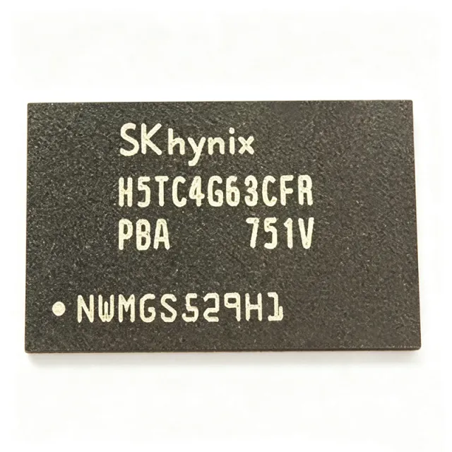
H5TC4G63CFR-PBA - 4Gb DDR3L SDRAM 256Mx16 | SK Hynix

The H5TC4G63CFR-PBA is a 4Gb DDR3L SDRAM organized as 256M x 16, manufactured by SK Hynix. It operates at VDD=VDDQ=1.35V with a tolerance of +0.100/-0.067V, enabling low-power operation for mobile and embedded systems. The device is housed in a 96-ball FBGA package (PBGA96) and is lead-free and halogen-free, fully RoHS compliant. DDR3L (Double Data Rate 3 Low Voltage) SDRAM is a type of synchronous dynamic random-access memory that operates at 1.35V, reducing power consumption by about 20% compared to standard DDR3 (1.5V). It is part of the DDR3 memory family, which uses double data rate signaling to transfer data on both edges of the clock, and is widely used in computing, networking, and industrial applications where power efficiency is critical. Key features include fully differential clock inputs (CK, CK) for improved signal integrity, differential data strobe (DQS, DQS) for precise data capture, and an on-chip DLL that aligns DQ, DQS, and DQS transitions with CK. The DM (data mask) function masks write data on both rising and falling edges, and the device supports auto precharge, auto self-refresh, and dynamic on-chip termination (ODT) for signal quality. The H5TC4G63CFR-PBA uses a CMOS process and includes ZQ calibration for output driver and ODT impedance matching, write leveling for command/address timing, and asynchronous reset for initialization. These features ensure reliable high-speed operation and simplify system design. Typical applications include DDR3L memory modules for laptops, embedded systems, networking equipment (routers, switches), and industrial PCs. Its low voltage and high density make it ideal for power-sensitive designs. When designing with this device, ensure proper decoupling and follow the PCB layout guidelines in the datasheet to maintain signal integrity at high frequencies. The device requires a stable 1.35V supply and careful termination of the differential clock and strobe lines.

USD $6.23 お問い合わせ
H5TC4G63CFR-PBL - 4Gb DDR3L SDRAM 256Mx16 | SK hynix
H5TC4G63CFR-PBL

H5TC4G63CFR-PBL - 4Gb DDR3L SDRAM 256Mx16 | SK hynix

The H5TC4G63CFR-PBL is a 4Gb DDR3L SDRAM (Double Data Rate 3 Low Voltage) memory chip from SK hynix, organized as 256M x 16 bits. It operates at a low voltage of 1.35V, making it ideal for power-sensitive applications such as mobile devices, embedded systems, and networking equipment. The device is available in a 96-ball FBGA package (TFBGA) and is lead-free and halogen-free, complying with RoHS standards. DDR3L SDRAM is a type of synchronous dynamic random-access memory that transfers data on both edges of the clock signal, doubling the data rate compared to single data rate SDRAM. The 'L' denotes low voltage operation at 1.35V, reducing power consumption by about 15% compared to standard DDR3 at 1.5V. This makes DDR3L a preferred choice for battery-powered and thermally constrained designs. Key features of the H5TC4G63CFR-PBL include a data rate of 1600 Mbps (PC3L-12800), a burst length of 8, and support for on-die termination (ODT) and posted CAS. The device also features auto refresh and self refresh modes, with a typical refresh period of 7.8 us at 85C. The 96-ball FBGA package provides a compact footprint suitable for high-density PCB layouts. The H5TC4G63CFR-PBL uses a high-performance CMOS process technology, ensuring fast access times and low power consumption. The memory array is organized into 8 banks, each with 32K rows, providing efficient row activation and precharge operations. The device supports a programmable CAS latency of 11, 12, and 13, allowing flexibility in system timing. Typical applications include main memory for laptops, ultrabooks, and embedded systems, as well as networking equipment such as routers and switches, and industrial automation controllers. The low voltage and high bandwidth make it suitable for applications requiring high memory density and low power. When designing with this device, ensure proper decoupling capacitors are placed near the VDD and VDDQ pins to minimize power supply noise. Also, follow the JEDEC DDR3L layout guidelines for signal integrity, especially for high-speed data lines.

見積もり お問い合わせ
H5TC4G63CFR-xxI - 4Gb DDR3L SDRAM | SK Hynix
H5TC4G63CFR-xxI

H5TC4G63CFR-xxI - 4Gb DDR3L SDRAM | SK Hynix

The H5TC4G63CFR-xxI is a 4Gb DDR3L SDRAM manufactured by SK Hynix, designed for main memory applications requiring high density, high bandwidth, and low power operation at 1.35V. It operates with VDD=VDDQ=1.35V +0.100/-0.067V, features fully differential clock inputs (CK, CK), differential data strobes (DQS, DQS), and an on-chip DLL to align DQ, DQS, and DQS transitions with CK. The device is lead-free and halogen-free, RoHS compliant, and comes in a 78-ball FBGA package. DDR3L (Double Data Rate 3 Low Voltage) SDRAM is a type of synchronous dynamic random-access memory that achieves high data transfer rates by transferring data on both edges of the clock signal. It operates at a lower voltage (1.35V) compared to standard DDR3 (1.5V), reducing power consumption by about 20% while maintaining similar performance. DDR3L is part of the DDR3 memory family, which is widely used in computing, networking, and embedded systems. Key features include a 4Gb density organized as 512M x 8, a data rate of [DATA_NEEDED: speed grade] (e.g., 1600 Mbps), and support for 1.35V operation. The device uses an 8n-prefetch architecture, which enables high bandwidth by fetching 8 data words per clock cycle. It also supports on-die termination (ODT), programmable CAS latency, and burst lengths of 8 and 4 (with burst chop). The H5TC4G63CFR-xxI is fabricated using advanced DRAM process technology, ensuring high reliability and low power consumption. The on-chip DLL synchronizes the output data with the clock, reducing skew and improving signal integrity. The device includes auto-refresh and self-refresh modes for low-power standby, and it supports temperature-compensated self-refresh (TCSR) to optimize refresh rate based on operating temperature. Typical applications include servers, networking equipment, industrial computing, and embedded systems where high memory density and low power are critical. The 1.35V operation makes it ideal for power-sensitive designs, such as laptops, portable devices, and energy-efficient data centers. When designing with this device, ensure proper decoupling of VDD and VDDQ with 0.1uF capacitors placed close to the pins. Follow the DDR3L layout guidelines for signal integrity, including matched trace lengths for DQ, DQS, and address/command signals. The device requires a stable 1.35V supply and a clean reference voltage (VREF) for optimal operation.

見積もり お問い合わせ
H5TC4G63CFR-xxJ - 4Gb DDR3L SDRAM 256Mx16 | SK Hynix
H5TC4G63CFR-xxJ

H5TC4G63CFR-xxJ - 4Gb DDR3L SDRAM 256Mx16 | SK Hynix

The H5TC4G63CFR-xxJ is a 4Gb DDR3L SDRAM manufactured by SK Hynix, organized as 256M x 16. It operates at a low supply voltage of VDD = VDDQ = 1.35V, making it ideal for power-sensitive applications such as mobile devices, embedded systems, and networking equipment. The device features fully differential clock inputs (CK, CK#), differential data strobes (DQS, DQS#), and an on-chip DLL that aligns DQ, DQS, and DQS# transitions with the CK transition. It is lead-free and halogen-free, compliant with RoHS standards. DDR3L SDRAM (Double Data Rate 3 Low Voltage) is a type of synchronous dynamic random-access memory that transfers data on both rising and falling edges of the clock signal, effectively doubling the data rate. DDR3L operates at 1.35V, reducing power consumption by about 20% compared to standard DDR3 (1.5V), while maintaining compatibility with DDR3 signaling levels. It is part of the memory hierarchy in computing systems, serving as main memory for processors, and is widely used in laptops, servers, and embedded applications. Key features include a 4Gb density, 16-bit I/O width, and support for various speed grades (e.g., -xxJ indicates a specific speed grade, likely 1600 Mbps or 1866 Mbps). The device uses a 96-ball FBGA package, which is standard for DDR3L SDRAM, ensuring compatibility with existing PCB designs. The operating temperature range is from 0°C to 95°C (case temperature), and it supports auto-refresh and self-refresh modes for power saving. Technically, the H5TC4G63CFR-xxJ employs an 8n-prefetch architecture, which allows high-speed data transfer by fetching 8 data bits per clock cycle per I/O. It includes programmable CAS latency, burst length (8 and 4 with burst chop), and on-die termination (ODT) for signal integrity. The device also supports write leveling and read leveling for improved timing margins in high-speed systems. Typical applications include main memory for laptops, ultrabooks, and embedded systems, as well as networking equipment like routers and switches, and industrial computing platforms. Its low voltage and high density make it suitable for power-constrained designs that require large memory capacity. When designing with this component, ensure proper decoupling capacitors near the VDD and VDDQ pins, and follow the DDR3L layout guidelines for signal integrity, including impedance matching and length matching for data and address lines. The device requires a stable 1.35V supply and a reference voltage (VREF) for the command/address bus.

見積もり お問い合わせ
H5TC4G63CFR-xxL - 4Gb DDR3L SDRAM 256Mx16 | SK Hynix
H5TC4G63CFR-xxL

H5TC4G63CFR-xxL - 4Gb DDR3L SDRAM 256Mx16 | SK Hynix

The H5TC4G63CFR-xxL is a 4Gb low power Double Data Rate III (DDR3L) Synchronous DRAM manufactured by SK Hynix. It is organized as 256M x 16 and operates at a low voltage of 1.35V, making it ideal for main memory applications that require large memory density, high bandwidth, and low power operation. The device is lead-free and halogen-free, compliant with RoHS standards, and is available in a 96-pin FBGA package. DDR3L SDRAM is a type of dynamic random-access memory that operates at a lower voltage (1.35V) compared to standard DDR3 (1.5V), reducing power consumption by approximately 20% while maintaining backward compatibility with DDR3-based environments. It is part of the DDR3 memory family, which uses double data rate signaling to transfer data on both edges of the clock, achieving high bandwidth. DDR3L is commonly used in laptops, embedded systems, and networking equipment where power efficiency is critical. Key features of the H5TC4G63CFR-xxL include a 4Gb density, 256M x 16 organization, 1.35V power supply, and support for data rates up to 2133 Mbps (depending on the speed grade). The device offers low power consumption, with a typical operating current of [DATA_NEEDED: IDD0] and standby current of [DATA_NEEDED: IDD2P]. It also features on-die termination (ODT), programmable CAS latency, and burst lengths of 8 and 4 (with burst chop). The device is designed for reliable operation over a temperature range of [DATA_NEEDED: operating temperature range]. The H5TC4G63CFR-xxL utilizes advanced DRAM process technology, providing high density and performance while minimizing power consumption. The 96-pin FBGA package offers excellent thermal and electrical characteristics, supporting high-speed signaling with minimal parasitic inductance. The device includes auto-refresh and self-refresh modes to maintain data integrity with minimal power draw. Typical applications include main memory for laptops and ultrabooks, embedded systems, networking equipment, and industrial computing. The low voltage and high bandwidth make it suitable for power-sensitive designs that require high performance. The device is also used in memory modules and system-on-module (SoM) designs. When designing with this component, ensure proper decoupling capacitors are placed near the power pins to minimize noise. The DDR3L interface requires careful PCB layout to maintain signal integrity, including matched trace lengths and controlled impedance. Refer to the SK Hynix datasheet for detailed design guidelines and timing parameters.

見積もり お問い合わせ
H5TC4G63MFR-PBA - 4Gb DDR3L SDRAM 256Mx16 | SK hynix
H5TC4G63MFR-PBA

H5TC4G63MFR-PBA - 4Gb DDR3L SDRAM 256Mx16 | SK hynix

The H5TC4G63MFR-PBA is a 4Gb DDR3L SDRAM organized as 256M x 16, manufactured by SK hynix. It operates at a supply voltage of 1.35V (VDD and VDDQ) with a range of +0.100V/-0.067V, and is housed in a 96-ball FBGA package. This memory device supports data rates up to 1866 Mbps (PC3L-14900) and is designed for low-power applications, offering a significant reduction in power consumption compared to standard DDR3. DDR3L SDRAM (Double Data Rate 3 Low Voltage) is a type of synchronous dynamic random-access memory that operates at 1.35V, reducing power consumption by about 20% compared to standard 1.5V DDR3. It is part of the DDR3 family, which uses double data rate architecture to transfer data on both edges of the clock, achieving high bandwidth. DDR3L is commonly used in mobile devices, embedded systems, and enterprise servers where power efficiency is critical. Key features include a 16-bit I/O configuration, 8 internal banks, and support for various burst lengths (BL8 and BL4 with burst chop). The device includes on-die termination (ODT), ZQ calibration, write leveling, and dynamic ODT for improved signal integrity. It also supports auto self-refresh and a temperature-compensated self-refresh rate to minimize standby power. The H5TC4G63MFR-PBA uses a 30nm-class process technology, enabling high density with low power. It features programmable CAS latency (CL), CAS write latency (CWL), and additive latency, allowing flexibility in system timing. The device is compliant with JEDEC DDR3L standards, ensuring interoperability with a wide range of controllers. Typical applications include mobile computing, networking equipment, industrial automation, and embedded systems where low power and high performance are required. Its 256Mx16 organization is ideal for systems needing a single high-density memory chip with a 16-bit data bus. When designing with this device, ensure proper decoupling capacitors near the power pins and follow the PCB layout guidelines in the datasheet to maintain signal integrity at high speeds. The device requires a stable 1.35V supply and careful termination of the address/control bus.

見積もり お問い合わせ
H5TQ2G63GFR-TEC - 2Gb DDR3 SDRAM 128Mx16 FBGA-96 | SK Hynix
H5TQ2G63GFR-TEC

H5TQ2G63GFR-TEC - 2Gb DDR3 SDRAM 128Mx16 FBGA-96 | SK Hynix

The SK Hynix H5TQ2G63GFR-TEC is a 2 Gigabit DDR3 SDRAM organized as 128M x 16 bits, with industrial -40C to +95C operating temperature support, in a 96-ball FBGA (PBGA-96) lead-free, halogen-free RoHS-compliant package. DDR3 SDRAM (Double Data Rate 3 Synchronous DRAM) is a CMOS dynamic random-access memory that transfers data on both rising and falling edges of a differential clock, doubling bandwidth versus single-data-rate designs. Within the memory hierarchy it sits below DDR4/DDR5 generations and above DDR2, and it remains the dominant DRAM class for cost-sensitive industrial, networking, and embedded main-memory designs requiring large density and high bandwidth on a 1.5V-class interface. Key features of the H5TQ2G63 family include fully synchronous operation referenced to both clock edges, auto self-refresh, an auto precharge function, an asynchronous reset function, data mask (DM) support for byte-wise write masking, dynamic on-die termination (ODT), ZQ calibration for output impedance matching, and write leveling for fly-by topology signal integrity. The -TEC speed-grade suffix denotes an extended industrial temperature rating, making this variant suitable for uncontrolled-environment systems. Architecturally, the device contains multiple banks with row activation, column read/write pipelines, and burst lengths of 8 (BL8) with on-the-fly addressing, as described in the manufacturer datasheet. Source data identifies the related H5TQ2G63DFR parts as 2,147,483,648-bit CMOS DDR3 SDRAMs operating at up to 933 MHz clock (DDR3-1866 class), ideally suited for main memory applications requiring large memory density and high bandwidth. Typical applications include embedded main memory for industrial controllers, networking and communication equipment, set-top boxes, and FPGA-based processing boards that implement DDR3 memory controllers. The x16 organization simplifies 16-bit and 32-bit wide memory subsystems with two devices. Design consideration: DDR3 signal integrity depends on length-matched routing, ODT configuration via mode registers, and correct ZQ calibration resistor placement; follow the reference routing guidelines in the manufacturer datasheet. This page synthesizes distributor pricing, same-family drop-in alternatives, application guidance, and design notes not found in the manufacturer datasheet.

見積もり お問い合わせ
H5TQ4G63AFR-H9C - 4Gb DDR3 SDRAM 256Mx16 | SK Hynix
H5TQ4G63AFR-H9C

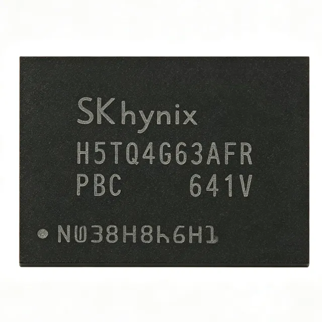
H5TQ4G63AFR-H9C - 4Gb DDR3 SDRAM 256Mx16 | SK Hynix

The H5TQ4G63AFR-H9C is a 4Gb CMOS Double Data Rate III (DDR3) Synchronous DRAM from SK Hynix, organized as 256M x 16. It operates at a clock speed of 0.255ns (tCK) and is packaged in a 96-ball TFBGA (Thin Fine-Pitch Ball Grid Array) with a rectangular shape. This device is designed for main memory applications requiring high density and bandwidth, offering fully synchronous operations referenced to both rising and falling edges of the clock. It supports a supply voltage of 1.5V and features 8192 refresh cycles, ensuring data integrity in high-performance computing environments. DDR3 SDRAM (Double Data Rate Type 3 Synchronous Dynamic Random-Access Memory) is a type of memory that transfers data on both edges of the clock signal, effectively doubling the data rate compared to single-data-rate SDRAM. It is a key component in the memory hierarchy, serving as the main system memory in computers, servers, and embedded systems. DDR3 is the successor to DDR2 and offers higher bandwidth and lower power consumption, making it suitable for a wide range of applications from consumer electronics to enterprise data centers. Key features of the H5TQ4G63AFR-H9C include a 4Gb density, 256M x 16 organization, and a 96-ball TFBGA package. It is halogen-free and RoHS compliant, meeting environmental standards. The device operates with a 1.5V power supply and supports a data rate of 0.255ns (approximately 3.9 Gbps per pin). The refresh cycle count of 8192 ensures reliable operation over extended periods. The package is designed for surface mount technology, enabling compact and high-density PCB layouts. Technically, the H5TQ4G63AFR-H9C utilizes advanced CMOS process technology to achieve high speed and low power. It features programmable CAS latency, burst length, and other timing parameters via the mode registers, allowing system designers to optimize performance. The device supports on-die termination (ODT) and dynamic ODT for improved signal integrity, which is critical at high data rates. The 96-ball TFBGA package provides excellent thermal and electrical performance, with a ball pitch of 0.8mm, facilitating routing and manufacturing. Typical applications for the H5TQ4G63AFR-H9C include desktop and laptop computers, servers, networking equipment, and embedded systems that require high-capacity, high-bandwidth memory. Its 256M x 16 organization is ideal for systems with a 16-bit data bus, such as many microprocessors and SoCs. The device's low power consumption and high reliability make it suitable for both consumer and industrial applications. When designing with this DDR3 SDRAM, it is essential to ensure proper signal integrity by following the layout guidelines for high-speed memory interfaces, including controlled impedance traces, proper termination, and decoupling. The memory controller must be configured to match the device's timing parameters, such as CAS latency and burst length, to achieve optimal performance. Additionally, thermal management should be considered, as high-speed operation can generate significant heat.

USD $6.50 お問い合わせ
H9JCNNNBK3MLYR-N6E - 16Gb LPDDR5-6400 SDRAM | SK Hynix
H9JCNNNBK3MLYR-N6E

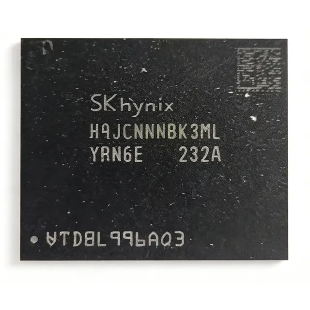
H9JCNNNBK3MLYR-N6E - 16Gb LPDDR5-6400 SDRAM | SK Hynix

The SK Hynix H9JCNNNBK3MLYR-N6E is a 16 Gb (2 GB) LPDDR5-6400 SDRAM organized as 512M x 32 with a 1.05 V core supply, housed in a 315-ball TFBGA package. It delivers a 6400 Mbps per-pin data rate over a dual-channel architecture, targeting high-bandwidth, power-sensitive mobile and embedded platforms. LPDDR5 (Low-Power Double Data Rate 5) is the fifth generation of the JEDEC low-power DRAM standard, positioned above LPDDR4X in the memory hierarchy: LPDDR5 SDRAM -> low-power DRAM -> DRAM -> volatile memory IC. Unlike standard DDR5 DIMM modules, LPDDR5 devices are soldered directly to the PCB, use a narrow 32-bit (x32) channel, and trade socketability for dramatically lower I/O power and a smaller footprint. The 1.05 V VDD2 rail is lower than the 1.1 V of LPDDR4X, which is the primary lever for reducing total memory power in battery-operated systems. Key differentiators of this part include its 6400 Mbps pin speed (a 33% uplift over LPDDR4X-4266), the 512M x 32 organization that maps cleanly onto 32-bit SoC memory controllers, and the TFBGA-315 ballout that is footprint-compatible across the SK Hynix LPDDR5 family. The device supports bank-group architecture and a low-power clock-stop mode for aggressive idle power reduction. Architecturally, the die uses SK Hynix's advanced 1-alpha-class DRAM process and integrates on-die termination (ODT), a programmable write-leveling scheme, and per-bank refresh to reduce peak current. The dual-channel x16+x16 internal split allows the controller to interleave accesses and hide refresh latency, which is critical for sustained bandwidth in AI inference and 4K video pipelines. Typical applications include flagship smartphones, automotive ADAS domain controllers, edge AI inference modules, 5G CPE and small cells, AR/VR headsets, and industrial machine-vision systems. In each case the 6400 Mbps rate and 1.05 V rail allow the SoC to hit its memory-bandwidth target without a discrete power penalty. A key design consideration is that LPDDR5 requires careful PCB trace-length matching and impedance control on the 32-bit data bus; unlike a DIMM, there is no module-level calibration, so signal integrity must be engineered at the board level. This page synthesizes distributor pricing, drop-in alternatives, and practical design notes not found in the manufacturer datasheet.

USD $24.37 お問い合わせ
H9JCNNNBK3MLYR-N6E - 16Gb LPDDR5-6400 SDRAM | SK Hynix
H9JCNNNBK3MLYR-N6E

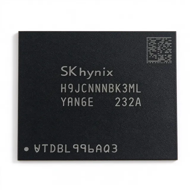
H9JCNNNBK3MLYR-N6E - 16Gb LPDDR5-6400 SDRAM | SK Hynix

The SK Hynix H9JCNNNBK3MLYR-N6E is a 16 Gb LPDDR5-6400 SDRAM organized 512M x 32 on a 16-bit data bus, supplied in a 315-ball TFBGA (TFBGA-315) surface-mount package and rated for data rates up to 6400 Mbps. It operates from a 1.05 V main supply (range 1.01 V to 1.12 V) with a 1.7 V to 1.95 V rail for the DRAM array, and is qualified to industrial thermal envelopes typical of mobile and embedded platforms. The device belongs to the SK Hynix H9JCNNN family of LPDDR5 products targeting power-sensitive, high-bandwidth applications. An LPDDR5 SDRAM (Low-Power Double Data Rate 5 Synchronous DRAM) is a JEDEC-defined volatile memory standard optimized for mobile and embedded systems where bandwidth density and energy per bit are the dominant design constraints. LPDDR5 succeeds LPDDR4/4X by adding sub-channels, higher per-pin data rates (up to 6400 Mbps/pin in this -N6E speed grade), improved command/address efficiency via ECC-on-command and dynamic frequency scaling, and a deep-sleep state for idle retention. In the broader hierarchy LPDDR5 sits under DRAM -> volatile memory -> semiconductor memory -> integrated circuit, and competes architecturally with LPDDR5X and DDR5 in mobile SoC designs. Key features of the H9JCNNNBK3MLYR-N6E include 6400 Mbps per-pin data rate, dual 16-bit sub-channels for a 32-bit logical interface, on-die temperature sensor, refresh management, and WriteX/ReadX training features defined by the LPDDR5 standard. The 315-ball TFBGA package is designed for high-density PCB layouts with matched-length routing, supporting both mobile form factors and embedded module designs. The H9JCNNNBK3MLYR-N6E is typically designed into smartphone application processors, AI edge inference modules, tablet SoCs, and automotive infotainment platforms where sustained memory bandwidth must be delivered within tight thermal envelopes. Its low-voltage operation and deep-sleep states also make it suitable for always-on inference and wearable compute. When designing with this part, observe JEDEC LPDDR5 PCB layout guidelines: matched impedance for command/address and data lanes, length matching within a sub-channel, decoupling concentrated near the package, and a clean 1.05 V LDO/DC-DC rail. Verify pin-out against the official SK Hynix datasheet before board fab to confirm the -N6E ball map. This page synthesizes distributor pricing, drop-in alternatives, and practical design notes that complement the SK Hynix datasheet, helping engineers validate BOM, footprint, and power budget decisions for LPDDR5-based designs.

USD $18.20 在庫あり
H9JCNNNBK3MLYR-N6E-SK - 16Gb LPDDR5-6400 SDRAM | SK Hynix | TFBGA-315
H9JCNNNBK3MLYR-N6E-SK

H9JCNNNBK3MLYR-N6E-SK - 16Gb LPDDR5-6400 SDRAM | SK Hynix | TFBGA-315

The SK Hynix H9JCNNNBK3MLYR-N6E-SK is a 16 Gigabit LPDDR5-6400 SDRAM organized as 512M x 32 in a 315-ball TFBGA surface-mount package, delivering up to 6400 Mbps per pin data rate over a 16-bit data bus. Operating from a 1.05 V core supply (rail range 1.01 V to 1.12 V) with a 1.7 V to 1.95 V supply for the I/O, it is engineered for high-bandwidth, power-sensitive mobile and embedded platforms. LPDDR5 (Low-Power Double Data Rate 5) SDRAM is a JEDEC-defined volatile memory standard designed as the successor to LPDDR4/4X for smartphones, tablets, ultra-thin notebooks, AI edge devices, and automotive infotainment. It belongs to the SDRAM -> DRAM -> volatile memory -> memory IC hierarchy. Compared with LPDDR4X, LPDDR5 doubles peak bandwidth to 6400 Mbps, introduces lower VDD voltages for energy efficiency, and adds on-die ECC and Decision Feedback Equalization (DFE) for signal integrity at high speeds. Key differentiating parameters include the 6400 Mbps data rate, 16-bit bus width, four-channel internal architecture, 1.05 V VDDQ, and an operating temperature range of -55C to +125C (industrial-grade, the widest grade in the H9JCNNN family). The device supports deep-sleep and power-down modes for sub-mW standby current. The 315-ball TFBGA package provides a low-profile footprint suitable for height-constrained mobile designs. The architecture is built on SK Hynix's advanced 1y-nm DRAM process, integrating the PMIC interface commands, frequency set, and refresh management defined by JEDEC JESD209-5. The dual-channel configuration enables parallel access for application processors, AI accelerators, and GPUs sharing the same memory pool. Built-in ECC mitigates single-bit soft errors at sub-20 nm nodes. Typical applications include flagship smartphone main memory, AI edge inference modules, ultra-thin notebook DRAM, automotive infotainment and ADAS platforms, and high-bandwidth industrial controllers. It pairs naturally with Snapdragon 8-series, MediaTek Dimensity, and Apple A-series application processors that natively support LPDDR5-6400 interfaces. Designers must route the 16-bit data bus as length-matched differential pairs with controlled impedance (typically 85 ohm differential), place a 0.1 uF + 1 uF decoupling capacitor network near each VDD/VDDQ ball, and follow SK Hynix reference PCB layout for the 315-ball TFBGA land pattern. The -SK suffix indicates SK Hynix branded reel/tray packaging. This page synthesizes distributor pricing, drop-in alternatives, and practical design notes not found in the standalone manufacturer datasheet, providing engineering value beyond simple spec repetition.

見積もり お問い合わせ
HA4-5002/883 - 110MHz Wideband Buffer Amplifier | Renesas
HA4-5002/883

HA4-5002/883 - 110MHz Wideband Buffer Amplifier | Renesas

The Renesas HA4-5002/883 is a monolithic, wideband, high slew rate, high output current buffer amplifier, qualified to MIL-STD-883 and housed in a 20-pin CLCC surface-mount package. It utilizes Intersil (formerly Harris) Dielectric Isolation technology to deliver 110 MHz of bandwidth, a typical slew rate of 1300 V/µs (1000 V/µs minimum), and a ±100 mA minimum output current capability enhanced by a 3 Ω output impedance. The 20-CLCC ceramic package makes it suitable for high-reliability military and aerospace programs that require hermetic packaging. A buffer amplifier (also called a unity-gain follower or current buffer) is a special-purpose analog building block placed between a high-impedance source and a low-impedance load. Buffers provide current gain without voltage gain, isolating upstream stages from load-induced disturbances such as cable capacitance, ADC input charge kickback, or laser diode nonlinear loading. In the broader taxonomy, the HA-5002 sits in the signal-chain hierarchy: sensor/transducer -> buffer -> ADC or driver -> downstream load. Buffer amplifiers complement operational amplifiers, which typically cannot source/sink the high peak currents needed for fast-settling, high-capacitance applications. Key features of the HA4-5002/883 include wideband 110 MHz operation, 1300 V/µs typical slew rate, ±100 mA minimum output current, 3 Ω output impedance, dielectric-isolation process for low parasitic latch-up susceptibility, and MIL-STD-883 Class B processing for high-reliability environments. The combination of speed and output drive makes it a classic choice for driving analog signals through long cables, laser diodes, and high-capacitance loads. Internally, the HA-5002 uses a complementary bipolar output stage with dielectric isolation, which prevents the substrate-junction latch-up common in junction-isolated high-current buffers. The wideband design uses local feedback and feedforward compensation paths that allow the closed-loop buffer to maintain flat gain and low distortion well past 10 MHz, even when driving 50 Ω or 100 Ω transmission lines. Typical applications include coaxial cable drivers, ADC front-end buffers, laser diode drivers, video line drivers, ATE (automatic test equipment) pin electronics, and reference buffers in precision instrumentation. Its MIL-STD-883 qualification also makes it suitable for avionics, missile guidance, and space-grade subsystems where commercial-grade plastic op amps are unacceptable. When designing with the HA4-5002/883, observe the thermal limitations of the 20-CLCC package: continuous ±100 mA output into a low impedance load produces noticeable self-heating, and supply bypassing must be placed immediately at the supply pins to sustain the high slew rate without ringing. This page synthesizes distributor pricing, drop-in and pin-compatible alternatives, and practical design notes not found in the manufacturer datasheet alone, helping procurement and design engineers quickly evaluate the HA4-5002/883 for new designs and legacy sustainment.

見積もり お問い合わせ
HC32L031 - 48MHz Cortex-M0+ 64KB Flash MCU | XHSC (小华)
HC32L031

HC32L031 - 48MHz Cortex-M0+ 64KB Flash MCU | XHSC (小华)

The XHSC (小华半导体) HC32L031 is a 32-bit ultra-low-power microcontroller based on the Arm Cortex-M0+ core running up to 48 MHz, integrating 64 KB of Flash and 8 KB of SRAM in compact LQFP-32 and QFN-32 (4x4 mm) packages. It operates from a wide 1.8 V to 5.5 V supply, making it suitable for both battery-powered and industrial 5 V rails. A low-dropout (LDO) linear regulator is an analog integrated circuit that maintains a tightly regulated output voltage even when the input-to-output voltage difference is small (the dropout voltage). LDOs belong to the broader family of linear regulators, which in turn are a subset of voltage regulators and power management ICs used in virtually every powered electronic system. The HC32L031 sits one level above: it is a microcontroller that *uses* internal LDOs to power its core and analog domains from a single external supply. Key differentiating features include a deeply engineered power management system with 0.65 µA Deep-Sleep current (all clocks off, IO retention, IO interrupt wake-up, full RAM/CPU state retention) and 45 µA/MHz active current at 3 V / 48 MHz with peripherals off. The device includes multiple low-power modes, an integrated LDO regulator, and Brown-Out Reset (BOR). Peripheral highlights include a 12-bit SAR ADC, multiple timers, UART, SPI, I²C, and an integrated LCD segment driver (variant dependent), making it highly competitive in metering and HMI applications. Architecturally, the HC32L031 leverages the Cortex-M0+ core (Thumb-2 instruction set, single-cycle IO) and pairs it with a high-efficiency on-chip voltage regulator to minimize dynamic power. The Flash is organized with erase/write protection to support secure in-field firmware updates. Typical applications include battery-powered IoT sensors, smart water/gas/heat meters, wearable health devices, low-power wireless sensor nodes, BLE/Zigbee beacon peripherals, electronic shelf labels, and consumer appliances requiring always-on sensing with multi-year battery life. Its wide 1.8 V–5.5 V input range also suits industrial 5 V control boards. When designing with the HC32L031, select the package variant (LQFP-32 F8TB or QFN-32 F8UB) that matches your PCB footprint and thermal target. Pay attention to decoupling: place 100 nF + 4.7 µF ceramic capacitors close to VDD/VSS pins to keep the internal LDO stable during load transients. This page synthesizes distributor pricing, package variants, drop-in alternatives, and practical design notes not consolidated in any single manufacturer datasheet, providing actionable engineering value for selection and procurement.

見積もり お問い合わせ
HCF4046M013TR - Micropower PLL, 1.4MHz, SOIC-16 | STMicroelectronics
HCF4046M013TR

HCF4046M013TR - Micropower PLL, 1.4MHz, SOIC-16 | STMicroelectronics

The STMicroelectronics HCF4046M013TR is a Micropower Phase-Locked Loop (PLL) IC operating at up to 1.4 MHz, housed in a 16-pin SOIC (0.154", 3.90mm width) package. It features quiescent current specified to 20V, very low power consumption of 70 µW (typ.) at VCO = 5V, and operating frequency range to 1.4 MHz (typ.) at VDD = 10V. The device also includes low frequency drift of 0.04%/°C (typ.) at VDD = 10V and a choice of two phase comparators: an exclusive-OR (XOR) detector and an edge-triggered sequential phase detector with charge pump output. A Phase-Locked Loop (PLL) is a closed-loop feedback system that generates an output signal whose phase is locked to the phase of an input reference signal. PLLs are widely used for frequency synthesis, modulation/demodulation, clock recovery, and tone decoding in analog and mixed-signal systems. As a member of the CMOS 4000-series logic family, the HCF4046 sits within the broader hierarchy of clock and timing integrated circuits (ICs), which also include phase-locked loops, frequency synthesizers, and clock generators. The 4046 architecture in particular is the industry-standard micropower PLL, with variants offered by multiple manufacturers. Key features of the HCF4046M013TR include a wide supply voltage range of 3V to 20V, very low quiescent current well-suited for battery-powered designs, two selectable phase comparators (Phase Comparator I for low-noise locking without dead zone, Phase Comparator II for high-noise rejection with a charge-pump output capable of driving low-pass filters), an on-chip linear VCO with external R/C tuning, and source-follower output buffer. The combination of low power, wide supply range, and dual phase comparators makes the device uniquely flexible among monolithic PLL ICs. The HCF4046 employs a CMOS architecture with an internal VCO whose gain is set by external resistor R1 and capacitor C1, and whose frequency offset is set by external R2 and C2. Phase Comparator I is an exclusive-OR gate offering low harmonic content in the locked condition but requiring 90° phase offset at the VCO input. Phase Comparator II is an edge-triggered sequential network that locks at zero phase error, allowing the loop to operate with arbitrary input duty cycles and providing a charge-pump output for direct connection to an external low-pass filter. The micropower CMOS design keeps dynamic supply current low even at maximum VCO frequency. Typical applications include FM demodulation and modulation, frequency synthesis, tone decoding, FSK (Frequency-Shift Keying) modems, motor speed control, and clock recovery from NRZ data. The wide supply range (3V to 20V) allows the device to operate directly from battery stacks, 5V logic rails, and ±15V analog supply rails with a single part number. When designing with the HCF4046M013TR, pay close attention to the loop-filter component selection, as it directly determines loop bandwidth, capture range, and lock time. Phase Comparator I requires 50% duty cycle signals for proper operation, whereas Phase Comparator II can handle any duty cycle. Bypass VDD with a 0.1 µF ceramic capacitor placed close to the IC pins to ensure clean supply rails. This page consolidates distributor pricing, verified pin-compatible drop-in alternatives, and practical loop-filter design guidance drawn from multiple sources rather than from the manufacturer datasheet alone.

見積もり お問い合わせ
HCF4093BE - Quad 2-Input NAND Schmitt Trigger | STMicroelectronics
HCF4093BE

HCF4093BE - Quad 2-Input NAND Schmitt Trigger | STMicroelectronics

The STMicroelectronics HCF4093BE is a CMOS quad 2-input NAND gate with Schmitt-trigger inputs, supplied in a 14-pin PDIP through-hole package. Each of the four independent gates performs the NAND function while exhibiting Schmitt-trigger hysteresis on both inputs, allowing slow or noisy edges to be cleaned into sharp, jitter-free logic transitions. The Schmitt trigger is a comparator-style input stage with two distinct switching thresholds: a higher positive-going threshold (VP) and a lower negative-going threshold (VN). The difference between them (VH = VP - VN) is defined as the hysteresis voltage. This built-in hysteresis makes the part ideal for conditioning slow analog or mechanical signals (RC oscillators, switch debouncing, sensor pulses) directly into clean logic levels without external comparators. The HCF4093 belongs to the 4000-series CMOS logic family, characterized by wide supply operation from 3 V to 18 V, low quiescent power consumption, and high noise immunity. Its four gates share common VDD and VSS pins. Each input is a standard CMOS inverter-style stage feeding a NAND tree, and outputs are buffered totem-pole drivers capable of sourcing/sinking typical 4000-series currents. As a CMOS part, all inputs include ESD-protection networks and should not be left floating. Typical applications include waveform and pulse shaping, monostable and astable multivibrators, line receivers for noisy environments, simple RC and crystal oscillators, and debounce circuits for mechanical switches. Hysteresis prevents multiple triggering on bouncing or slowly rising edges, eliminating the need for external Schmitt-trigger comparator stages. When designing with this device, observe standard CMOS handling: tie unused inputs to VDD or VSS (never leave them open) and place a 0.1 uF decoupling capacitor as close as possible to the VDD pin. Output drive capability is moderate (a few mA), so check fan-out when driving multiple loads or long traces.

見積もり お問い合わせ
HCS361-I/P - KEELOQ Code Hopping Encoder, 8-PDIP | Microchip
HCS361-I/P

HCS361-I/P - KEELOQ Code Hopping Encoder, 8-PDIP | Microchip

The Microchip Technology HCS361-I/P is a code hopping encoder that pairs a 28-/32-bit programmable serial number with a 64-bit programmable encryption key to produce a 67-bit transmission frame (32-bit hopping code + 35-bit fixed code) for unidirectional Remote Keyless Entry (RKE) and access-control systems. Packaged in an 8-pin PDIP through-hole outline and rated for operation from 2.0 V to 6.6 V (per Microchip datasheet) or 3.0 V to 6.9 V (per some distributor listings), it ships as a -40 °C to +85 °C industrial-grade part with the “-I” temperature suffix and the “/P” PDIP package suffix. A code hopping encoder is a security-focused transmitter IC that transmits a different encrypted code on every button press, defeating simple replay attacks. It belongs to the broader category of encoders/decoders/multiplexers (logic ICs), and within Microchip's portfolio it is a member of the KEELOQ family — a hierarchy that runs encoder -> KEELOQ hopping encoder -> security transmitter IC -> logic IC -> integrated circuit. The HCS361 sits between the lower-cost HCS300/HCS301 and newer HCS362/HCS365 devices, balancing small package outline, low BOM cost, and patented hopping-code security. Key features include 28/32-bit serial number programming, 64-bit encryption key storage in EEPROM, unique 67-bit transmission per button event, three button inputs (S0/S1/S2), a 4-word (S0..S3 with PWM) option (per family datasheet), low standby current for battery-powered fobs, automatic code-word synchronization, and Microchip's patented KEELOQ learning algorithm so a paired receiver only needs to remember the last transmitted code. HCS361-I/P is the industrial temperature (-40 °C to +85 °C) variant in the through-hole PDIP-8 footprint. The device uses Microchip's KEELOQ nonlinear block-cipher algorithm with a 64-bit manufacturer key and a 16/20-bit discriminator. On every button press the encoder generates a fresh 32-bit hopping code by combining the counter value, the button bitmap, and the encrypted discriminator; the receiver validates the rolling counter and decrypts the discriminator before accepting the transmission, providing strong replay-attack immunity for garage-door openers, gate controls, alarm panels, and automotive RKE. Typical applications include garage-door and gate openers, automotive Remote Keyless Entry transmitters, wireless doorbells, alarm and security system keypads, asset-tracking fobs, and industrial access-control handheld remotes. Pair it with a Microchip HCS compatible receiver decoder (e.g., the receiver side of the HCS family) to complete a one-way secure link. When designing with the HCS361-I/P, observe the VDD decoupling guidance from the datasheet (a 0.1 µF ceramic cap close to the VDD pin), the RF section layout for the companion transmitter PCB, and the four-button debounce pattern in Microchip application notes. The industrial -40 °C to +85 °C range makes this part suitable for outdoor fobs and unheated enclosures, while the through-hole PDIP-8 package simplifies hand-soldering and prototype builds. This page synthesizes distributor pricing, drop-in package alternatives, and practical design notes not found in the manufacturer datasheet alone.

見積もり お問い合わせ
HCTL-2001-A00 - CMOS Quadrature Decoder/Counter IC | Broadcom
HCTL-2001-A00

HCTL-2001-A00 - CMOS Quadrature Decoder/Counter IC | Broadcom

The Broadcom HCTL-2001-A00 is a CMOS quadrature decoder and counter interface IC designed to convert quadrature signals from a rotary encoder directly into a 32-bit digital count accessible to a host microcontroller. Housed in a 16-pin PDIP package, the device operates from a single 4.5V to 5.5V supply at up to 14 MHz clock frequency and integrates a digital noise filter, a 32-bit up/down counter, and an 8-bit three-state bus interface. It is specified for industrial temperature ranges of -40C to +85C and is intended to offload time-intensive quadrature-decoding tasks from microcontrollers in digital closed-loop motion-control systems. A quadrature decoder IC is a specialized interface that resolves two phase-shifted square-wave channels (often called CHA and CHB) from an incremental optical or magnetic rotary encoder into direction-aware digital position counts. This function sits in the motion-control signal chain between the encoder transducer and the host processor, where it replaces software decoding loops with deterministic hardware counting and noise rejection. Quadrature decoders belong to the broader family of sensor and detector interface ICs, with close relatives including incremental encoder counters, motion-control coprocessors, and motor-position feedback interfaces. Key features of the HCTL-2001-A00 include 32-bit counter resolution, programmable digital filtering on the quadrature inputs to reject noise below a configurable pulse-width threshold, an 8-bit multiplexed data bus with chip-select and read strobe, a cascade output for multi-axis chaining via the HCTL-2021, and a TTL/CMOS-compatible interface. The integrated noise filter eliminates the need for external RC debouncing on encoder channels and improves reliability in electrically noisy industrial environments such as stepper-servo drive cabinets and CNC machinery. The HCTL-2001-A00 is built on a low-power CMOS process with TTL-compatible inputs and three-state outputs, achieving 14 MHz internal operation while drawing only a few milliamps. The architecture separates noise-filtered quadrature decoding, the 32-bit latch, and the bus interface into independent functional blocks, allowing simultaneous count updates and host reads. The cascade architecture, when used with the HCTL-2021-A00 companion, supports longer word lengths or dual-axis counting without glue logic. Internally the chip implements a divide-by-n filter and a synchronized state machine that prevents missed counts at high encoder speeds. Typical applications include closed-loop servo motor position feedback, CNC machine tool axis encoders, robotics odometry wheels, digital input systems reading rotary selectors, printer and plotter carriage position tracking, and incremental-encoder-to-microprocessor interfaces in industrial automation. In a stepper-servo drive, the IC converts a 1000-line encoder into a precise 4000-count-per-revolution position word, freeing the MCU for trajectory and PID calculation rather than interrupt-driven counting. When designing with the HCTL-2001-A00, observe the layout guidelines in the Avago (now Broadcom) AV01-0041EN datasheet: place 0.1 uF decoupling close to VCC, keep encoder traces short and twisted-pair, and use the cascade signals when chaining with HCTL-2021 for longer count widths. Designers should also enable the noise filter at the highest practical time constant that still preserves the maximum encoder pulse width, balancing noise immunity against maximum countable shaft speed. This page synthesizes distributor stock data from DigiKey, Mouser, and Octopart, drop-in HCTL-20xx family alternatives, and practical design guidance not consolidated on the manufacturer datasheet.

見積もり お問い合わせ
HD3SS3212IRKSR - 10Gbps USB 3.1 Type-C 2:1 Mux | TI
HD3SS3212IRKSR

HD3SS3212IRKSR - 10Gbps USB 3.1 Type-C 2:1 Mux | TI

The Texas Instruments HD3SS3212IRKSR is a high-speed bidirectional passive switch configured as a 2:1 multiplexer or 1:2 demultiplexer, supporting USB 3.1 Gen 1 (5 Gbps) and Gen 2 (10 Gbps) data rates in a 20-pin VQFN (2.5x4.5 mm, RKS) package. It is designed primarily for USB Type-C applications where the role of a USB-C port's high-speed lanes is dynamically toggled between a USB 3.1 host/device and an alternate-mode accessory (DisplayPort, debug, etc.). The device carries two differential channels between Port A and either Port B or Port C, with channel selection driven by a single SEL control pin, and operates from a 3.0 V to 3.6 V single supply with only 20 µA typical quiescent current. What is a passive differential mux? A passive differential multiplexer/demultiplexer is an analog switch that routes high-speed differential pairs without active redriver or retimer circuitry. Unlike a redriver, a passive mux introduces only insertion loss and a small amount of return-loss variation - it does not restore signal amplitude. This makes passive muxes ideal for short-reach intra-chassis routing where the channel loss budget is already met, but problematic for long cables or lossy connectors. The HD3SS3212 sits in the signal-chain hierarchy between the USB-C receptacle and the host/device PHY: PHY -> redriver (optional) -> mux/demux -> connector. Key features include 10 Gbps differential signal bandwidth, low on-resistance (Ron) of typically 5 ohm, -3 dB bandwidth above 7 GHz, ESD protection of 2 kV HBM on high-speed pins, and a flow-through pinout that simplifies PCB layout. The wide -3 dB bandwidth ensures signal-integrity margin for USB 3.1 Gen 2 compliance, while the flow-through pinout keeps TX and RX differential pairs on a straight horizontal trace, eliminating the need for vias in the high-speed path. Architecture is built on TI's high-speed analog switch process, optimized for low capacitance (typically < 1.5 pF per channel) and minimal channel-to-channel skew. The device is bidirectional and symmetric - either side can act as the common port - which simplifies both mux and demux use cases. The SEL input is a standard CMOS logic pin with an internal pull-down, defaulting to Port B at power-up. Typical applications include USB Type-C ports on laptops, tablets, and smartphones; docking stations; DisplayPort alt-mode adapters; Thunderbolt 3/4 accessory switches; and any platform that needs to share a USB-C connector between USB and a non-USB high-speed interface. Design considerations: place the HD3SS3212 as close to the USB-C receptacle as possible to keep stub lengths below 200 mil. Use 90 ohm differential impedance with reference-grounded coplanar-waveguide routing, AC-couple the channels with 100 nF capacitors at the PHY side, and provide a clean 3.3 V rail decoupled with 0.1 µF + 1 µF ceramics. This page synthesizes distributor pricing, drop-in pin-compatible alternatives, parametric comparison, and PCB-level design notes beyond the manufacturer datasheet.

見積もり お問い合わせ
HD3SS3220LRNHR - 10Gbps USB 3.1 Type-C 2:1 Mux with DRP | TI
HD3SS3220LRNHR

HD3SS3220LRNHR - 10Gbps USB 3.1 Type-C 2:1 Mux with DRP | TI

The Texas Instruments HD3SS3220LRNHR is a 10 Gbps USB 3.1 Gen 2 Type-C 2:1 mux with an integrated Dual Role Port (DRP) controller, housed in a 30-pin WQFN (RNH) package measuring 4.5 mm x 2.5 mm. The device supports SuperSpeed USB signaling up to 10 Gbps and provides Channel Configuration (CC) logic plus 5 V VCONN sourcing for Type-C ecosystems. It operates from a single 3.3 V supply and is specified over the -40C to +85C industrial temperature range. A USB Type-C DRP port controller is a specialized interface IC that detects USB Type-C cable orientation, manages CC pin attach/detach logic, advertises port roles (DFP, UFP, or DRP), and routes high-speed SuperSpeed differential pairs through an integrated 2:1 mux. The HD3SS3220 sits within the broader USB Type-C interface hierarchy: Type-C controller -> USB 3.1 mux -> high-speed signal switch -> signal conditioning. This category sits above basic USB 2.0 switches and below full USB PD controllers in functional complexity. Key features include the integrated 2:1 SuperSpeed mux that eliminates external discrete crosspoint switches, automatic DRP toggle with configurable Try.SNK / Try.SRC behavior, integrated 5 V VCONN switch with overcurrent protection, BC 1.2 (Battery Charging) support, and I2C interface for role and mux control. The WQFN-30 (RNH) package provides a low-impedance thermal path through the exposed pad, enabling operation in space-constrained designs without external heatsinking. The HD3SS3220 uses a CMOS process with on-die termination for the high-speed channels, achieving <3 dB insertion loss at 5 GHz and channel-to-channel skew typically below 2 ps. The integrated CC logic block handles attach/detach state machine, role detection, and VCONN fault recovery autonomously, reducing firmware burden on the host controller. Spread-spectrum clocking on the internal reference minimizes EMI peaks to ease FCC compliance in docking station and monitor designs. Typical applications include USB Type-C docks, hub downstream ports, notebook Type-C ports, monitor USB inputs, and tablet charging-only or DRP ports. The wide role-configuration flexibility makes it especially well suited to multifunction docks that must toggle between host and device behavior depending on attached accessory. When designing with this part, ensure the high-speed SuperSpeed traces are length-matched within 150 mil and routed with 85 ohm differential impedance. The exposed pad must be soldered to a continuous ground plane for both thermal dissipation and signal return-path integrity; insufficient ground stitching causes insertion loss degradation above 5 GHz. This page synthesizes distributor pricing, drop-in alternatives, and practical design guidance not found in the manufacturer datasheet alone.

見積もり お問い合わせ
HD4074818FS - 4-Bit OTP Microcontroller with LCD Driver | Renesas
HD4074818FS

HD4074818FS - 4-Bit OTP Microcontroller with LCD Driver | Renesas

The Renesas HD4074818FS is a 4-bit single-chip microcomputer with on-chip OTPROM, an integrated 16-digit LCD driver/controller, an analog voltage comparator, and a 32 kHz watch oscillator circuit, packaged in an 81-pin QFP (FS suffix). It is part of the legacy HD407xxxx OTPROM family originally developed by Hitachi Semiconductor and now maintained by Renesas Electronics following the merger of Hitachi's and Mitsubishi's semiconductor operations. A 4-bit microcontroller (4-bit MCU) is a class of single-chip microcomputer whose central processing unit operates on 4-bit data words, with typical 8-bit or 16-bit internal addressing. These MCUs were widely adopted in the 1990s and early 2000s for cost-sensitive, low-power, embedded control tasks where 4-bit arithmetic precision was sufficient - household appliances, remote controls, calculators, electronic meters, simple LCD-display appliances, and consumer white goods. In the modern semiconductor taxonomy, the 4-bit MCU is a hypernym under microcontroller (MCU), then embedded processor, then integrated circuit. The HD4074818FS is differentiated by its integrated 16-digit LCD driver, which eliminates the need for an external LCD controller chip in many small-format display products. Key features of the HD4074818FS include: an OTPROM program memory for one-time field programmability, integrated LCD segment driver supporting up to 16 digits, an on-chip voltage comparator for analog signal conditioning, a 32 kHz watch oscillator for low-power real-time-clock (RTC) operation, and multiple I/O ports. The FS suffix denotes the QFP package, which provides a large pin count suitable for the LCD segment outputs and parallel I/O. The device operates from a single low-voltage supply and is engineered for ultra-low standby current consumption. Architecturally, the HD4074818FS combines a 4-bit ALU core with dedicated LCD-driver hardware, a 32 kHz crystal oscillator for timekeeping, and analog comparator peripherals. This single-chip integration reduces BOM cost and PCB footprint in products that previously required a separate MCU, LCD driver IC, and comparator IC. The OTPROM program memory allows late-stage customization of firmware after the silicon is fabricated, which was a key advantage over mask-ROM 4-bit MCUs of the same era. Typical applications include: home appliance controllers (rice cookers, microwave ovens, washing machines), electronic thermostats, water heaters, simple digital scales, remote control units with LCD displays, and battery-powered consumer devices requiring a low-cost LCD readout. Designers should note that this part belongs to a mature legacy family - verify current lifecycle status and long-term supply before committing to a new design. The 81-pin QFP package requires careful PCB layout for reliable soldering. This page synthesizes distributor pricing, lifecycle status, drop-in alternatives, and practical design notes not consolidated in any single manufacturer datasheet.

見積もり お問い合わせ
HD6417750RF240 - SH7750R 240MHz SuperH RISC MCU | Renesas
HD6417750RF240

HD6417750RF240 - SH7750R 240MHz SuperH RISC MCU | Renesas

The Renesas HD6417750RF240 is a 32-bit SuperH RISC (SH-4) microprocessor (MPU) running at 240 MHz, supplied in a 208-pin PQFP package with a 1.4 V to 1.6 V core supply and a 3.0 V to 3.6 V I/O supply, providing ROMless operation with 48K x 8 of on-chip RAM. A microprocessor (MPU) is a VLSI central processing unit on a single chip that integrates the CPU core, caches, MMU, bus interfaces, and peripheral controllers. The SH7750R belongs to the SuperH family: a RISC microprocessor architecture -> 32-bit RISC processor -> embedded microprocessor -> system-on-chip class MPU -> semiconductor IC. This taxonomy situates the HD6417750RF240 within the broader processor hierarchy that scales up to application processors for desktops and down to microcontrollers for deeply embedded sensing. Key features include a 240 MHz CPU clock with object-code upward compatibility from SH-1, SH-2, and SH-3, 16 KB instruction cache, 32 KB data cache (32 KB unified in SH-4), an integrated MMU with 4-way set-associative TLB, a single-precision IEEE-754 floating-point unit, a 16-bit unified instruction set, and a 32-bit external bus interface supporting SDRAM, SRAM, ROM, and PCMCIA. The 208-pin PQFP (28 mm x 28 mm) package offers a familiar through-hole-style lead footprint suitable for legacy industrial designs and evaluation boards. The HD6417750R architecture combines a Harvard-style cache hierarchy with a unified external bus, enabling high-throughput data movement for embedded computing workloads such as real-time control, machine vision front-ends, and high-resolution graphical HMI. The integrated FPU and MMU allow full Linux and Windows CE operating-system support, which is rare among 32-bit embedded MPUs of this generation. Typical applications include industrial machine controllers, factory automation HMIs, in-vehicle infotainment prototypes, network-attached print/image processing engines, point-of-sale terminals, and legacy SH-4 upgrade boards. The 240 MHz performance is well matched to QVGA/VGA-resolution graphics and MPEG-2 decode. When designing with the HD6417750RF240, pay close attention to the dual-voltage power tree (1.5 V core, 3.3 V I/O), the SDRAM interface timing, and bus-arbiter configuration for any DMAC peripherals. Refer to the Renesas SH7750R hardware manual for PLL loop filter components and reset sequencing. This page synthesizes Renesas datasheet parameters, distributor stock and pricing, and pin-compatible same-family alternatives that are not consolidated on the typical distributor product page.

見積もり お問い合わせ
HD6417750RX240V - SH-4 240MHz 32-Bit MPU, 208-QFP | Renesas
HD6417750RX240V

HD6417750RX240V - SH-4 240MHz 32-Bit MPU, 208-QFP | Renesas

The Renesas HD6417750RX240V is a 32-bit SH-4 (SuperH) RISC microprocessor running at 240 MHz in a 208-pin LQFP package with a 3.3 V I/O supply, ROMless architecture, and Pb-free lead finish. An MPU (Microprocessor Unit) in this category is a 32-bit superscalar RISC core that executes the SuperH instruction set and connects to external SDRAM, SRAM, and ROM through an external bus interface. The HD6417750RX240V belongs to the SH7750 family and sits at the top of the embedded processing hierarchy between microcontroller units (MCU) and full application processors, with explicit multimedia (MMU, cache, FPU) extensions. SH-4 cores have been used in set-top boxes, printers, industrial control, and automotive infotainment where deterministic 32-bit performance exceeds what 8/16-bit controllers can deliver. Key features of the HD6417750RX240V include a 240 MHz CPU clock, an integrated FPU, separate 16 KB instruction and 8 KB data caches, an MMU with TLB, and an external bus interface supporting SDRAM, PCMCIA, and burst ROM. The 208-pin LQFP package exposes all of these signals plus serial, USB, and timer peripherals, allowing a compact PCB layout without BGA complexity. The architecture combines a dual-issue superscalar pipeline with a Harvard-style cache structure, achieving roughly 360 MIPS / 1.4 GFLOPS sustained throughput at 240 MHz. On-chip peripherals include DMA, SCI (UART), timers, and a PCMCIA controller, which is unusual for embedded MPUs of this class. The part is fabricated in a low-power CMOS process that lets designers hold the core in software-controlled standby while keeping external bus monitoring active. Typical applications include industrial machine controllers, point-of-sale terminals, set-top box media decoders, and OEM printer/copier controllers. The 240 MHz speed and FPU make it well suited for JPEG/MPEG-1 software codecs and for the control loops in office imaging equipment. When designing with this part, remember that it is ROMless - boot firmware must reside in external flash or ROM. Provide a PLL loop filter network per the hardware manual and observe the 3.3 V supply tolerance (typically +/-5%) to keep the PLL locked across temperature. The LQFP package simplifies rework versus BGAs in legacy industrial designs. This page synthesizes distributor pricing, same-family SH-4 drop-in alternatives, and practical design notes not assembled in the manufacturer datasheet alone.

見積もり お問い合わせ
HD6417750SX167V - 167MHz SH-4 32-Bit Microprocessor | Renesas
HD6417750SX167V

HD6417750SX167V - 167MHz SH-4 32-Bit Microprocessor | Renesas

The Renesas HD6417750SX167V is a 32-bit RISC microprocessor based on the SuperH SH-4 (SH7750) core, clocked at 167 MHz and packaged in a 208-pin LQFP (S-V) form factor with ROMless architecture. As part of the SuperH family, it integrates a 32-bit single-core SH-4 CPU with on-chip FPU, 32 KB instruction cache, 32 KB data cache, and a sophisticated bus state controller (BSC) capable of glueless external memory interfacing. The device targets embedded applications requiring high processing throughput with low power consumption in industrial, office automation, and networking equipment. An SH-4 SuperH microprocessor belongs to the superscalar RISC CPU family originally developed by Hitachi and now maintained by Renesas Electronics Corporation. The SH-4 instruction set extends the earlier SH-1/SH-2 ISA with 16-bit fixed-length instructions and adds a 128-bit media extension (SIMD-style) for multimedia and DSP-style workloads. Within the broader semiconductor taxonomy, the SH7750 sits in the hierarchy: SH-4 core -> SuperH family -> 32-bit RISC microcontroller -> embedded processor -> semiconductor IC. The ROMless designation means the chip executes code from external NOR flash, SRAM, or SDRAM, providing maximum firmware flexibility for long-lifecycle industrial designs. Key differentiating features include 167 MHz sustained core frequency, hardware IEEE 754 single-precision floating-point unit, integrated memory management unit (MMU) supporting virtual memory, separate 32 KB instruction and 32 KB data caches with write-back policy, and a peripheral set encompassing DMAC, timer, SCI, and a powerful 32-bit external bus. The on-chip FPU executes single-precision floating-point in one cycle for SIMD instructions and supports vector arithmetic. With five-stage pipeline architecture and dual-issue superscalar dispatch, the SH-4 delivers up to 360 MIPS / 1.4 GFLOPS peak throughput, enabling real-time video, audio, and control processing without external co-processors. Typical applications include industrial machine controllers, networked printers, multifunction office imaging systems, set-top box controllers, point-of-sale terminals, and embedded HMI panels. The wide 32-bit external bus and SDRAM controller support high-bandwidth data movement required for image scanning and printing pipelines. The integrated MMU enables full Linux and Windows CE operating system support, opening the device to open-software stacks used in commercial embedded products. When designing with this part, allocate sufficient PCB area for the 208-pin LQFP and ensure the external memory bus traces are length-matched for SDRAM operation above 100 MHz. The device requires a 3.3 V I/O supply and a separate core voltage rail; decoupling must follow Renesas reference layout for stable PLL lock. This page synthesizes distributor stock, drop-in alternatives from the SH7750 family, and practical design notes not consolidated in the manufacturer datasheet alone.

見積もり お問い合わせ
HD64F3687GFPV - H8/300H 16-bit MCU, 56KB Flash, 20MHz | Renesas
HD64F3687GFPV

HD64F3687GFPV - H8/300H 16-bit MCU, 56KB Flash, 20MHz | Renesas

The Renesas HD64F3687GFPV is a 16-bit single-chip microcontroller belonging to the H8/300H Tiny Series of the H8/3687 Group, integrating a high-performance H8/300H CPU core with 56KB of on-chip Flash memory and packaged in a 64-pin LQFP (10x10 mm, 0.5 mm pitch). It operates from a 4V to 5.5V supply and runs up to 20 MHz, offering 53 I/O pins for moderate-complexity embedded designs. What is an H8/300H microcontroller? The H8/300H is Renesas' enhanced 16-bit CISC CPU family, upward-object-code-compatible with the original H8/300 while adding a wider 16-bit register file and richer addressing modes. Tiny-Series derivatives such as the H8/3687 Group position this MCU in the hierarchy: H8 family -> H8/300 CPU -> H8/300H Tiny -> H8/3687 Group, used as mainstream microcontrollers -> embedded systems -> semiconductor ICs. The Flash variant (-F suffix) integrates user-programmable Flash memory suitable for prototyping and field-upgradable production firmware. Key features include on-chip Flash program memory, RAM, multiple timers (16-bit and 8-bit), a watchdog timer, and serial interfaces including SCI (asynchronous/synchronous) and I2C bus. The H8/300H core executes most instructions in 2 to 4 states at 20 MHz, achieving roughly 5 to 10 MIPS sustained throughput. The 64-LQFP package exposes a wide parallel I/O bus and dedicated peripheral pins, enabling direct LED/segment-LCD driving, motor control PWM, and external memory interfacing when required. Typical applications include white-goods motor control (washing machines, air conditioners), consumer appliance key-scan user interfaces, industrial sensor signal conditioning, and small home appliances requiring deterministic real-time control. The integrated timers and SCI/I2C allow direct connection to sensors, inverters, and operator panels without external glue logic. When designing with this device, follow the H8/3687 Group hardware manual for unused-pin handling (tie all unused CMOS inputs to VCC or GND to prevent pass-through current). Designers migrating from earlier H8/300 parts benefit from object-level upward compatibility for firmware reuse.

見積もり お問い合わせ