製品 (39,000+)

MC9S12XS256CAE - 16-bit S12X MCU 256KB Flash 40MHz | NXP
MC9S12XS256CAE

MC9S12XS256CAE - 16-bit S12X MCU 256KB Flash 40MHz | NXP

The NXP MC9S12XS256CAE is a 16-bit microcontroller from the S12XS family, featuring the HCS12X core running at up to 40 MHz, 256 KB of on-chip Flash program memory, and a 64-pin LQFP (10x10 mm) package. It is optimized for cost-sensitive automotive body electronics applications and integrates CAN, SCI, and SPI connectivity on-chip. An MCU (microcontroller unit) is a single-chip computer containing a CPU core, program and data memory, peripherals, and I/O. The 16-bit MCU category sits between 8-bit microcontrollers (used for simple control) and 32-bit Cortex-M/ARM cores (used for complex compute). Within the broader taxonomy, MC9S12XS256CAE belongs to: MCU -> 16-bit MCU -> HCS12X core MCU -> S12XS automotive MCU family -> NXP Freescale legacy S12X lineage -> semiconductor. Key features include 256 KB of Flash, an integrated CAN (Controller Area Network) module for automotive networking, multiple timers including PWM and ECT, an 8/10/12-bit ADC, and on-chip voltage regulator supporting a wide supply range. The S12XS family provides hardware and software compatibility across the S12X platform, allowing code and PCB reuse. The device supports up to 59 I/O ports and includes background debug mode (BDM) for non-intrusive in-circuit debugging. Architecturally, the HCS12X core extends the HCS12 with an enhanced XGATE peripheral co-processor (not enabled on this 64-pin derivative), a 16-bit CPU with enhanced indexed addressing, and a modular memory map. The 64-LQFP package (10x10 mm body, 0.5 mm pitch) gives the device a footprint suitable for body-electronics modules where compact PCB layout and AEC-Q100 grade are required. Typical applications include automotive body control modules (BCM), instrument clusters, HVAC controllers, seat and door zone modules, and lighting controllers. The wide operating temperature range (-40C to +85C industrial grade; +125C available on other S12XS variants) and integrated CAN make it a strong fit for in-vehicle networking. When designing with the MC9S12XS256CAE, ensure the BDM interface is broken out to a 6-pin header for development, since field firmware updates rely on this access path. Decouple the internal regulator output with at least 1 uF ceramic close to the VDD pins, and route the analog supply (VDDA) separately from the digital VDD to minimize ADC noise coupling. This page synthesizes distributor pricing, drop-in S12XS family alternatives, and practical engineering notes not found in the manufacturer datasheet alone.

見積もり お問い合わせ
MC9S12XS64MAE - 16-bit 40MHz 64KB Flash HCS12X MCU | NXP
MC9S12XS64MAE

MC9S12XS64MAE - 16-bit 40MHz 64KB Flash HCS12X MCU | NXP

The NXP MC9S12XS64MAE is a 16-bit HCS12X microcontroller built around the S12X core running at 40 MHz, integrating 64 KB of on-chip Flash and 4 KB of RAM into a 64-pin LQFP (10x10 mm) package. The HCS12X architecture augments the original HCS12 instruction set with a co-processor-style XGATE peripheral accelerator, which offloads interrupt-driven tasks without loading the main CPU, making the MC9S12XS64MAE well-suited to real-time automotive body-electronics applications. An automotive-grade microcontroller (MCU) is a programmable processor designed for the harsh electrical and thermal environments of vehicles; specifically, the MC9S12XS64MAE is part of the S12XS family that lives in the body-comronics layer of the in-vehicle hierarchy. It targets cost-sensitive body-electronics domains such as body controllers, gateway nodes, seat controllers and HVAC panels where deterministic real-time behaviour and CAN connectivity are essential. Key features include 64 KB of Flash program memory, 1 KB EEPROM and 4 KB SRAM, an integrated 6-channel PWM, an 8-channel 10-bit ADC, two SCI (UART) ports, one SPI port, one I2C port, CAN 2.0 A/B support, and up to 59 general-purpose I/O lines. The device supports a supply voltage range of 1.72 V to 1.98 V (core) with typical 5 V I/O operation and an operating temperature range of -40 C to +125 C as required by automotive under-hood and cabin specs. The HCS12X core executes S12 instructions at 40 MHz with up to 50 ns instruction time, while the XGATE peripheral co-processor handles deterministic interrupt requests (IRQs) at up to 80 MHz, allowing the MC9S12XS64MAE to handle complex protocol stacks and sensor-fusion tasks in real time. The combination of high-resolution timer, fast ADC conversion, and XGATE-driven DMA makes it a strong solution for body-electronics timing-critical loops. Typical uses include automotive body controllers, CAN-based gateway nodes, instrument clusters, HVAC control modules, seat-control ECUs, and body-comfort modules where S12X scalability and software reuse across the NXP family is desired. In industrial applications it is also useful for motor-control boards and PLC I/O expansion cards that require a 16-bit processor and CAN. When designing with this MCU, ensure adequate decoupling on VDDR/VSS (1 uF + 100 nF bulk) and provide a clock source compatible with the integrated PLL (4-16 MHz crystal). Use the BDM (Background Debug Mode) interface for in-circuit programming and - for safety-critical applications - follow NXP's AN2419 guidelines on locking the Flash security feature. This page synthesizes distributor pricing, same-package drop-in alternatives such as MC9S12XS128MAE, comparison parameters and practical design notes - value not found in the manufacturer datasheet alone.

見積もり お問い合わせ
MC9SDG128ECPV-FR - 50MHz 128KB Flash HCS12X MCU | Freescale
MC9SDG128ECPV-FR

MC9SDG128ECPV-FR - 50MHz 128KB Flash HCS12X MCU | Freescale

The Freescale Semiconductor MC9SDG128ECPV-FR is a 16-bit HCS12X microcontroller operating at 50 MHz, with 128 KB of flash memory organized as 128K x 8, in a 112-LQFP 20 x 20 mm package. It belongs to the HCS12X family and combines a 50 MHz processor core with embedded flash, CANbus connectivity, EBI/EMI, and SPI according to the verified distributor data. The part is identified as a Rochester Electronics/Freescale Semiconductor offering, so procurement and traceability should be confirmed against the manufacturer and authorized distribution records. An HCS12X microcontroller is a 16-bit embedded microcontroller, a member of the broader MCU -> embedded processor -> semiconductor hierarchy. MCUs integrate a processor core, memory, peripherals, and communication interfaces into one device for control-oriented products. This HCS12X device is suited to systems that require a deterministic embedded controller, local flash-resident firmware, and serial interfaces rather than a host-class processor or general-purpose application processor. The verified listing identifies the key architectural value points as 16-bit core width, 50 MHz operating frequency, 128 KB flash, 128K x 8 organization, 112-LQFP packaging, and connectivity including CANbus, EBI/EMI, and SPI. These figures establish a compact embedded-control platform for automotive, industrial, communications, and appliance designs. The listed package is a surface-mount LQFP with 112 pins and a 20 x 20 mm body, offering a high pin count for peripheral and bus access. Compared with an 8-bit MCU, the 16-bit HCS12X architecture provides a wider native data path and higher clock capability. Compared with a host processor, it remains purpose-built around embedded control, peripherals, and deterministic firmware execution. The flash capacity allows a substantial amount of control code and configuration data to reside on-chip, while the documented serial connectivity supports communication with sensors, actuators, external memory, and system modules. Typical uses include automotive body and powertrain-adjacent control modules, industrial automation controllers, CAN-based equipment, motor-control subsystems, communication interfaces, and embedded test fixtures. System designers should verify peripheral assignments, electrical limits, timing, clocking, memory organization, and software-device support against the official MC9SDG128ECPV datasheet before layout release. A practical design consideration is that the 112-LQFP footprint requires careful escape routing and a defined thermal strategy. Keep power and ground connections short, route sensitive clock and communication signals away from noisy switching paths, and validate the PCB stack-up and assembly process. This page combines verified distributor snippets, cross-reference observations, and engineering guidance; it does not infer undocumented electrical limits or pin functions. This product page also distinguishes verified facts from missing datasheet detail. It is useful for initial part selection and sourcing, but final schematic, firmware, pinout, and timing decisions require the official manufacturer documentation.

見積もり お問い合わせ
MC9SDG128ECPVR2-FR - 16-Bit 50MHz 128KB MCU | NXP
MC9SDG128ECPVR2-FR

MC9SDG128ECPVR2-FR - 16-Bit 50MHz 128KB MCU | NXP

The NXP Semiconductors MC9SDG128ECPVR2-FR is a 16-bit HCS12X microcontroller with a 50 MHz core, 128 KB of flash memory, and a 112-LQFP 20 mm × 20 mm package. It combines an embedded automotive-oriented control architecture with connectivity identified in verified comparisons as CANbus, EBI/EMI, SPI, and I²C. The -FR orderable variant is associated with the -FR ordering information supplied by the distributor record, while the broader MC9SDG128ECPVR2 family is associated with Freescale Semiconductor, now part of NXP Semiconductors. A microcontroller is a programmable semiconductor that integrates a processor core, memory, and peripherals on one device. The MC9SDG128ECPVR2-FR belongs to the HCS12X family and is positioned above general-purpose logic and basic 8-bit microcontrollers for applications requiring more processing performance, embedded flash, and dedicated serial interfaces. Its 16-bit word architecture and 50 MHz maximum speed make it suitable for automotive control modules, body electronics, actuator controllers, and industrial embedded systems where deterministic control and multiple peripheral functions are important. Verified data confirms 128 KB of flash memory, a 16-bit CPU, 50 MHz operation, and a 112-LQFP package. Comparison data also identifies HCS12X connectivity including CANbus, EBI/EMI, SPI, and I²C. Electrical limits, SRAM capacity, ADC resolution, timer details, supply voltage, current consumption, temperature range, watchdog behavior, and package dimensions beyond the stated 20 mm × 20 mm package were not supplied in the verified dataset and must be confirmed from the manufacturer datasheet before design release. The 112-LQFP package provides a high pin count relative to smaller MCU packages, supporting a broader mix of digital and analog functions while remaining a surface-mount solution. Its 20 mm × 20 mm footprint is considerably larger than compact QFN devices, so PCB designers should preserve the exact pin map, exposed thermal requirements, and recommended land pattern. The large package can simplify routing in designs with many external sensors and actuators, but it increases board area and requires careful decoupling and thermal planning. Typical uses include automotive body-control modules, CAN-connected sensor nodes, actuator interfaces, instrument-cluster electronics, industrial automation controllers, and communication gateways. The verified 50 MHz rating and HCS12X platform provide useful performance for protocol handling and real-time control, while 128 KB flash supports embedded application code. Design engineers should verify peripheral availability, pin multiplexing, clocking, memory map, electrical limits, and toolchain support in the datasheet before selecting it for a new platform. This page consolidates verified distributor specifications, package information, sourcing links, and design-oriented guidance. It does not infer undocumented electrical values, pin names, lifecycle claims, or a guaranteed replacement. For production procurement, confirm authorized distribution, stock status, firmware and software-tool compatibility, and lifecycle status with the manufacturer or an authorized distributor.

見積もり お問い合わせ
MC9SDG128EVPVR2 - 16-Bit 50MHz 128KB Flash MCU 112-LQFP | Freescale/NXP
MC9SDG128EVPVR2

MC9SDG128EVPVR2 - 16-Bit 50MHz 128KB Flash MCU 112-LQFP | Freescale/NXP

The NXP (formerly Freescale) MC9SDG128EVPVR2 is a 16-bit microcontroller from the HC12 (CPU12) family, integrating 128KB of Flash program memory and operating at up to 50 MHz, housed in a 112-pin LQFP package measuring 20 mm x 20 mm. According to the distributor datasheet description, it combines a 16-bit CPU12 core with on-chip Flash (128K x 8) and is qualified for extended-temperature industrial embedded applications. Background: A microcontroller (MCU) is a single-chip computer that integrates a CPU core, program memory (Flash/ROM), data memory (RAM), and programmable peripherals. The CPU12 architecture is an enhanced 16-bit superset of the original Motorola HC11, designed for automotive and industrial real-time control with a BDM (Background Debug Mode) interface, hardware-multiply/divide, and a paged memory model. Within the broader taxonomy, an MCU sits between a microprocessor (which requires external memory) and an SoC (which integrates even more system functions on the same die). Key features: the 50 MHz core delivers up to 50 MIPS of integer throughput with deterministic interrupt latency, while the integrated 128KB Flash supports in-application programming for field firmware updates. The 112-LQFP (20x20 mm) package exposes enough I/O for multi-channel ADC, PWM, CAN, SPI, and SCI peripherals typical of the S12DG sub-family, and the extended-temperature grade suits under-hood and industrial enclosures. Technical depth: the S12 architecture uses a 16-bit data path with a 20-bit program counter, supporting a 1MB linear address space with bank-switched Flash pages. Hardware breakpoints, BDM, and on-chip EEPROM emulation via Flash partitioning simplify development, while built-in periodic interrupt timers and a real-time interrupt (RTI) provide OS-free task scheduling for safety-critical automotive ECUs. Typical applications for this part include automotive body and chassis control modules, CAN/J1850 gateway nodes, instrumentation clusters, HVAC controllers, and industrial sensor-conditioning boards where 16-bit deterministic control outperforms 8-bit MCUs but full 32-bit Cortex-M is unnecessary. Design consideration: at 50 MHz the core draws significant current transients; place four 100 nF decoupling capacitors as close as possible to the VDD/VSS pin groups and reserve a dedicated ground plane under the 112-LQFP thermal pad for EMC-sensitive CAN bus designs. Boundary-scan is not supported - validate production firmware with a BDM probe on at least one test pad. This page consolidates current distributor pricing, validated drop-in alternatives from the same S12 family, and practical design notes not duplicated in stock-page listings, helping engineers extend legacy designs without a costly board respin.

見積もり お問い合わせ
MC9SDG256BCFUR2 - 16-Bit 50MHz 256KB Flash MCU | NXP
MC9SDG256BCFUR2

MC9SDG256BCFUR2 - 16-Bit 50MHz 256KB Flash MCU | NXP

The NXP Semiconductors MC9SDG256BCFUR2 is a 16-bit CPU12 microcontroller operating at 50 MHz, with 256 KB of flash memory organized as 256K x 8, in an 80-QFP 14 x 14 mm package. It is a member of the HCS12 family and is identified by the retrieved distributor data as an embedded microcontroller suitable for automotive and industrial control systems. The supplied records identify the device as Freescale Semiconductor MC9SDG256BCFUR2, with NXP as the current manufacturer context. A microcontroller is a semiconductor device that integrates a processor core, memory, peripheral interfaces, and control logic into one package. In the hierarchy of electronic components, this CPU12 device belongs to the embedded-controller, microcontroller, and semiconductor categories. Its flash memory supports firmware storage, while its 16-bit CPU architecture and 50 MHz operating frequency provide a defined platform for real-time control, communication, timing, and peripheral-intensive products. The verified data confirms the principal product attributes: 16-bit CPU12 architecture, 50 MHz operation, 256 KB flash memory, 256K x 8 organization, and an 80-QFP package measuring 14 x 14 mm. The same product is also described in one retrieved distributor result as a 25 MHz PQFP80 embedded microcontroller, creating a frequency discrepancy that requires confirmation against the manufacturer datasheet before design release. Other electrical ratings, pin functions, memory maps, peripheral resources, and environmental limits are not included in the supplied verified data. MC9SDG256BCFUR2 is relevant to embedded automotive electronics, industrial controllers, communication modules, motor-control systems, and other products requiring a compact 80-lead microcontroller. The package size and pin count provide a defined PCB footprint, but exact pin assignments cannot be reproduced safely without the complete manufacturer pinout. Firmware developers should also verify clock, memory, peripheral, and electrical details against the official HCS12 documentation before selecting pull-ups, decoupling, external interfaces, or production test procedures. The primary design consideration is source validation. Because the retrieved records disagree on operating frequency and do not provide a complete electrical specification table, engineers should confirm the authoritative datasheet, errata, and device qualification information for the exact ordering code. This page preserves supplied values exactly and identifies unavailable parameters rather than inferring them from related CPU12 devices. This product data combines distributor identification, package information, sourcing context, and engineering caveats. It supports initial BOM research while explicitly separating verified facts from data needed for schematic design, firmware integration, PCB layout, and production qualification.

見積もり お問い合わせ
MC9SDJ128BCFUR2 - 16-Bit 50MHz 128KB Flash MCU | NXP
MC9SDJ128BCFUR2

MC9SDJ128BCFUR2 - 16-Bit 50MHz 128KB Flash MCU | NXP

The NXP Semiconductors MC9SDJ128BCFUR2 is a 16-bit CPU12 microcontroller rated at 50 MHz with 128 KB of flash memory in an 80-QFP 14 x 14 mm package. It belongs to the MC9S12D family of embedded processors and controllers, combining a 50 MHz core, on-chip flash, and integrated microcontroller peripherals in one device. The supplied distributor records identify the device as a CPU12 microcontroller with 128K x 8 flash organization and an 80-QFP package. A microcontroller is a semiconductor that integrates a processor core, memory, and peripherals such as timers, serial interfaces, analog blocks, and interrupt controllers. In the broader hierarchy, it is an embedded processor and controller within the semiconductor and integrated-circuit categories. The CPU12 architecture is designed for control-oriented embedded systems where deterministic peripheral access, interrupt handling, and compact software support are important. The MC9SDJ128BCFUR2 is therefore positioned between a general-purpose host processor and a small resource-constrained microcontroller. The principal verified feature set is a 16-bit CPU12 core operating at 50 MHz, 128 KB of flash memory, and an 80-QFP package measuring 14 x 14 mm. These figures make the part suitable for embedded control systems that need more flash capacity than a very small microcontroller while retaining a dedicated single-chip architecture. The distributor listings also identify the device as an MCU rather than a discrete logic or power component. Detailed supply voltage, memory-map, peripheral, timing, and temperature parameters are not included in the supplied verified records and require the manufacturer datasheet for final design confirmation. Typical applications include industrial control, motor and motion control, automotive electronics, communications equipment, and instrumentation. In these systems, the 50 MHz CPU12 core can execute control software, the 128 KB flash region can store firmware, and the 80-QFP package provides a conventional surface-mount assembly format. Firmware selection, memory-map compatibility, peripheral availability, electrical limits, and package pin assignments must be checked before production use. Designers should preserve the exact CPU12 memory map and pin configuration when creating a replacement strategy. Because the verified data does not confirm an official manufacturer datasheet URL, pin names, electrical ratings, or lifecycle designation, those details should remain subject to engineering verification rather than inference. This page combines the verified distributor identity, package and memory information, sourcing links, and design-oriented guidance without fabricating unprovided electrical values. This page distinguishes the MC9SDJ128BCFUR2 from generic MCU alternatives by documenting the verified 16-bit architecture, 50 MHz operating frequency, 128 KB flash capacity, and 80-QFP package. For purchasing and design decisions, compare the complete manufacturer datasheet and application requirements with the verified distributor listings, especially when firmware, pinout, temperature grade, supply voltage, or production status must be guaranteed.

見積もり お問い合わせ
MC9SDT128BMPVR2 - 16-bit 25MHz 128KB MCU | NXP
MC9SDT128BMPVR2

MC9SDT128BMPVR2 - 16-bit 25MHz 128KB MCU | NXP

The NXP Semiconductors MC9SDT128BMPVR2 is a 16-bit HCS12 CISC microcontroller operating at 25 MHz with 128 KB of embedded Flash memory in a 112-pin LQFP package. The verified distributor listing identifies it as an embedded microcontroller from Freescale Semiconductor, now part of NXP, and reports an in-stock offering from Hotenda. Its combination of embedded Flash, a 16-bit architecture, and a high-pin-count LQFP makes it suitable for industrial embedded control systems requiring broad external peripheral connectivity. A microcontroller is a programmable semiconductor that integrates a CPU core, memory, and peripherals into one device. This MCU belongs to the embedded-controller hierarchy and specifically to the 16-bit HCS12 family. Unlike an 8-bit microcontroller, the 16-bit CPU is designed to process wider data values and more demanding control tasks. The available evidence identifies the MC9SDT128BMPVR2 specifically as a 16-bit HCS12 CISC MCU with 128 KB Flash, while several electrical, memory-map, and peripheral details remain unverified. The principal verified features are a 25 MHz operating frequency, 16-bit HCS12 CISC architecture, and 128 KB embedded Flash. Distributor descriptions classify the device as an embedded microcontroller and list it in LQFP packaging. These parameters distinguish it from smaller-memory 8-bit devices and from microcontrollers using more advanced processor architectures, but they do not by themselves establish software compatibility with another MCU family. The 112-pin LQFP package offers substantially more connection points than a small leaded controller package. That package position is useful when a system needs numerous external I/O lines, communication channels, timers, or mixed-signal interfaces. Exact pin functions, I/O counts, electrical limits, clocking, memory map, and peripheral inventory must be checked against the official device documentation before schematic or PCB design. Potential uses include industrial equipment controllers, motor and motion-control systems, automotive or transportation electronics, data-acquisition equipment, and embedded products that need substantial I/O capacity. The 128 KB Flash figure supports a meaningful firmware footprint, although RAM size, flash endurance, write timing, and bootloader capabilities are not present in the supplied evidence. The primary procurement warning is lifecycle and software risk. The listings mix Freescale Semiconductor, NXP Semiconductors, Rochester Electronics, and third-party suppliers, so authenticity, date code, traceability, and original manufacturer status should be confirmed before production use. Existing firmware should also be checked for peripheral, register, interrupt-vector, and memory-layout compatibility before replacement. This page consolidates verified source snippets, transparent specification gaps, procurement considerations, and engineering-selection guidance. It does not infer an official datasheet URL, electrical limits, pinout, qualification status, or drop-in replacement where the supplied data does not establish those facts.

見積もり お問い合わせ
MC9SDT256BCPVR2 - 256KB HCS12 Microcontroller | NXP
MC9SDT256BCPVR2

MC9SDT256BCPVR2 - 256KB HCS12 Microcontroller | NXP

The NXP Semiconductors MC9SDT256BCPVR2 is a 16-bit HCS12 CISC microcontroller with 256KB flash memory, supplied in a 48-pin LQFP package. The verified distributor information identifies it as an embedded microcontroller rather than a general-purpose logic or analog device. Its integrated flash program memory supports firmware storage, while the HCS12 architecture provides the execution core for embedded control, communications, and industrial equipment designs. The CPV package designation corresponds to the 48-pin LQFP outline, although individual signal assignments and electrical limits are not present in the supplied search results and must be checked against the manufacturer datasheet before layout or firmware release. A microcontroller is a semiconductor that integrates a processor core, memory, peripherals, and I/O in one package. A 16-bit HCS12 device belongs to the embedded-microcontroller hierarchy, where deterministic control software and hardware peripherals replace a separate desktop processor and support circuitry. The MC9SDT256BCPVR2 is intended for applications requiring embedded code storage and compact packaged control electronics. Its architectural classification and flash capacity are confirmed by the verified distributor listing, but core frequency, voltage range, RAM size, peripheral set, temperature range, and package dimensions are not specified in the supplied data. The principal confirmed feature is 256KB of embedded flash. This storage capacity can hold bootloader code, application logic, calibration data, and protocol handlers in a single controller package, reducing the need for external program-memory devices. The HCS12 CISC instruction set and integrated microcontroller resources are useful for embedded systems where predictable control flow and compact hardware integration matter. Because detailed clock and memory specifications are unavailable here, design engineers should not assume processing performance, interrupt behavior, or peripheral availability without consulting the official MC9SDT256B documentation. The part is positioned for industrial embedded control, motor and actuator management, instrumentation, communications equipment, and compact controller platforms. In each case, the MCU would execute real-time control software and interface with external sensors, drivers, or communications transceivers. The LCSC listing reports RoHS data and a price of $47.1171, while DigiKey identifies Rochester Electronics as the listed supplier and indicates that the part can be ordered. Inventory and lifecycle status should therefore be confirmed at procurement time rather than inferred from marketplace search results. A replacement or alternate design should be selected only after confirming the exact package outline, pin mapping, supply voltage, clock configuration, memory map, peripheral set, and software compatibility. The verified cross-reference results contain generic tools but do not identify a manufacturer-confirmed, pin-to-pin substitute. Therefore, engineers should treat any candidate as a redesign candidate until its documentation demonstrates compatibility. The MC9SDT256BCPVR2 is best approached as a controlled embedded-platform component with procurement and lifecycle validation required before volume production.

見積もり お問い合わせ
MC9SXDP512VPVR2 - 16-Bit 512KB Automotive MCU | NXP
MC9SXDP512VPVR2

MC9SXDP512VPVR2 - 16-Bit 512KB Automotive MCU | NXP

The NXP Semiconductors MC9SXDP512VPVR2 is an automotive-oriented 16-bit S12X microcontroller with 512 KB of programmable flash in a 112-pin LQFP package. It is associated with the MC9S12XDP512 family, which targets automotive multiplexing applications and combines 32-bit-class performance with the efficiency of a 16-bit MCU architecture. The exact operating voltage, clock, SRAM, peripheral set, temperature range, and pin functions were not supplied in the verified data and require confirmation from the manufacturer documentation. A microcontroller, or MCU, integrates a processor core, nonvolatile program memory, volatile data memory, peripherals, and interrupt control on one semiconductor device. Within the product hierarchy, this component is an MCU → embedded processor → semiconductor. S12X devices are designed for real-time control systems where deterministic peripheral access and integrated communication resources can reduce external component count compared with a separate processor and support devices. The available evidence identifies the MC9S12XDP512 family as targeting automotive multiplexing. That use case commonly requires multiple communication interfaces, real-time control, and dependable peripheral integration, although individual CAN, LIN, SPI, SCI, timer, and I/O counts must be verified against the exact datasheet. The VPVR2 ordering code also selects a specific package, temperature, performance, and qualification configuration, so it should not be inferred solely from the base family name. MC9SXDP512VPVR2 is sold through multiple distributors, but the verified search results provide inconsistent lifecycle and sourcing descriptions. DigiKey lists the part through Rochester Electronics, while other listings identify NXP USA or Freescale Semiconductor. Buyers should therefore verify authorized status, date code, flash write cycles, qualification grade, and manufacturer traceability before production release. The 512 KB flash capacity makes this MCU relevant to automotive body, multiplexing, gateway, and distributed control designs where protocol stacks and application logic require more program memory than a small 8-bit MCU. Engineers should confirm memory maps, peripheral multiplexing, pin assignments, clocking, and electrical limits against the exact MC9S12XDP512 manufacturer datasheet before schematic capture or firmware migration. PCB implementation should preserve the package dimensions, exposed thermal strategy, and recommended high-speed layout constraints documented for the 112-pin LQFP. Because no verified pinout or complete electrical characterization appears in the supplied results, no pin, voltage, current, timing, or thermal value should be inferred from the family description alone. The supplied listing evidence supports procurement research, but it is not a substitute for the exact manufacturer datasheet. This page consolidates the verified distributor links, supplier pricing, family positioning, and source limitations while explicitly separating known facts from missing technical data. That distinction helps engineers qualify the device for automotive multiplexing without treating unverified generic MCU assumptions as MC9SXDP512VPVR2 specifications.

見積もり お問い合わせ
MCF51AC128ACFUE - 32-bit ColdFire V1 MCU 128KB Flash | NXP
MCF51AC128ACFUE

MCF51AC128ACFUE - 32-bit ColdFire V1 MCU 128KB Flash | NXP

The NXP MCF51AC128ACFUE is a 32-bit ColdFire V1 microcontroller delivering up to 50 MHz core speed with 128 KB of embedded Flash and up to 16 KB of SRAM, housed in a 64-pin QFP package (14x14 mm). It belongs to the MCF51AC Flexis series, which provides pin-, peripheral-, and tool-compatible 8-bit S08AC and 32-bit ColdFire V1 devices, enabling seamless migration as system complexity grows. Key features include the V1 ColdFire core with single-cycle multiply-accumulate (MAC) instructions, an integrated analog chain with up to 16-channel 12-bit ADC, multiple timers including a 6-channel PWM, and communication peripherals covering SCI (UART), SPI, and I2C. The 50 MHz core and 128 KB Flash make it well-matched to industrial control, motor drive, and human-machine interface (HMI) applications that demand real-time deterministic performance. The MCF51AC family is also notable for its 5V-tolerant I/O and on-chip voltage regulator, supporting 2.7V to 5.5V operation from a single rail. This simplifies power-tree design in 5V-dominated industrial systems. The wide operating range and integrated peripherals position the MCF51AC128ACFUE as a workhorse MCU for mid-range embedded designs. Typical applications include industrial motor control (BLDC and stepper), smart metering, HVAC control, building automation, point-of-sale terminals, and medical instrumentation. The 12-bit ADC, PWM channels, and SCI/SPI interface are well-suited to closed-loop control loops where deterministic latency is required. When designing with this MCU, plan oscillator and decoupling layout early: place a 100 nF decoupling cap adjacent to every VDD pin, and route the externally supplied RESET signal with a guard trace. The internal voltage regulator requires a bulk cap on the VREG pin per the manufacturer datasheet typical-application circuit. The MCF51AC128ACFUE is approaching end-of-life per NXP lifecycle announcements. Engineers designing new platforms should consult the latest NXP PCN documents and evaluate the suggested replacement, the MCF51AC128CCFUE (the 'C' suffix denotes the latest silicon revision). For reference and upgrade planning, this page consolidates distributor pricing, drop-in compatible alternatives, lifecycle status, and PCB design notes not found on a single distributor page.

見積もり お問い合わせ
MCF51AC128AVFUE - 50MHz 128KB Flash 32-Bit MCU | NXP
MCF51AC128AVFUE

MCF51AC128AVFUE - 50MHz 128KB Flash 32-Bit MCU | NXP

The NXP MCF51AC128AVFUE is a 32-bit ColdFire V1 microcontroller with a 50 MHz operating frequency, 128 KB of Flash memory, and a 64-QFP package measuring 14 mm by 14 mm. The device is designed for embedded systems that require 32-bit processing, compact packaging, and compatibility with the Flexis controller family. Its 3.3 V and 5 V operating support is identified in the verified product data, while detailed electrical limits and peripheral specifications must be confirmed in the manufacturer datasheet. A microcontroller is a programmable semiconductor that integrates a processor core, memory, and peripherals into one device. The ColdFire architecture uses a variable-length reduced instruction set computer design, allowing compact code while providing 32-bit processing capability. The MCF51AC family belongs to the Flexis series, where 8-bit and 32-bit controller options support migration and shared hardware concepts. This positioning makes the MCF51AC128AVFUE relevant to industrial controls, appliances, data acquisition equipment, and connected embedded products. The verified listing identifies the MCU as part of the MCF51AC family and specifies a 50 MHz maximum clock, 128 KB Flash, and 64-QFP package. The 128 KB Flash figure corresponds to 128K by 8 bits according to the distributor description. Because the supplied snippets do not provide RAM size, pin-level functions, ADC specifications, timer resources, operating-temperature limits, or electrical absolute-maximum ratings, those values are retained as data-needed items rather than inferred. The ColdFire V1 core is suitable for embedded control workloads requiring deterministic digital processing, interrupt-driven peripherals, and moderate code density. The 50 MHz clock provides a useful performance envelope for protocol handling, state machines, motor or appliance control, and supervisory logic. Actual application suitability depends on the peripheral mix, memory map, timing, and pin multiplexing documented in the manufacturer datasheet. The 64-QFP package exposes more pins than a small QFN and can simplify access to external interfaces, subject to the verified pinout. Typical designs can use the MCU for industrial control boards, motor-control supervisory circuits, building equipment, test instruments, and low-to-medium complexity consumer products. Designers should verify clock configuration, power sequencing, reset behavior, and all peripheral electrical limits against the official documentation before layout release. The QFP package should be paired with a footprint that matches the exact 14 mm by 14 mm outline and pin pitch. A key sourcing consideration is lifecycle status. The supplied distributor results show active purchasing pages and list the part for sale, but they do not provide a current manufacturer lifecycle declaration. Confirm stock, lead time, and authorized-channel status with the manufacturer or an authorized distributor before committing to production. This page distinguishes verified facts from unavailable technical parameters.

見積もり お問い合わせ
MCF51AC128CCPUE - 32-Bit 50MHz 128KB MCU | NXP
MCF51AC128CCPUE

MCF51AC128CCPUE - 32-Bit 50MHz 128KB MCU | NXP

The NXP Semiconductors MCF51AC128CCPUE is a 32-bit ColdFire V1 microcontroller operating at 50 MHz, with 128 KB of flash memory and a 64-LQFP 10 x 10 mm package. The device is identified with 54 programmable I/O pins and is supplied for industrial-temperature operation from -40°C to 85°C. Its 2.7 V to 5.5 V operating range supports embedded control systems that use 3.3 V or 5 V power rails. According to the verified distributor and comparison data, the MCU belongs to the MCF51AC family and shares a 64-pin surface-mount footprint. A microcontroller such as the MCF51AC128CCPUE integrates a processor core, flash program memory, digital I/O, timers, and communication peripherals on one integrated circuit. The ColdFire V1 core belongs to the 32-bit RISC microcontroller hierarchy, combining instruction-level control with dedicated hardware peripherals. In the broader electronics system, this device sits between a simple digital controller and a more complex processor: it can execute embedded firmware, read inputs, operate actuators, and coordinate communication without requiring a separate external memory device for its 128 KB program storage. The principal verified features are a 50 MHz maximum clock, 128 KB of flash, 54 programmable I/O pins, a 2.7 V to 5.5 V supply range, and LVD, PWM, and WDT peripherals. The 64-LQFP package provides 64 physical terminals and a defined gull-wing surface-mount form. The 50 MHz operating point is useful for deterministic control loops, while the 128 KB flash capacity provides room for application firmware. The stated PWM, watchdog, and low-voltage detection functions support robust embedded-control designs. The MCF51AC family is presented in the verified data as pin-, peripheral-, and tool-compatible with selected 8-bit S08AC128 devices. This compatibility can reduce migration effort when a product transitions between supported controller architectures, although the exact firmware, memory-map, electrical, and peripheral requirements must be verified against the relevant datasheet before substitution. One verified comparison listing identifies a 50.33 MHz frequency figure, while the distributor result identifies 50 MHz; the nominal 50 MHz value is used here without extrapolating beyond the supplied data. Typical applications include industrial automation, consumer electronics, embedded motor and power-control systems, communication modules, and general-purpose control boards. Its 54 programmable I/O pins are particularly useful when the design needs multiple digital interfaces, status indicators, sensing inputs, or actuator outputs. The 3.3 V and 5 V supply compatibility also makes it relevant to mixed-voltage industrial and consumer equipment, provided the external circuit respects the device-specific limits in the manufacturer datasheet. Designers should confirm every pin function, supply sequencing requirement, clock configuration, peripheral assignment, and package-specific constraint against the exact MCF51AC128CCPUE datasheet before production release. PCB layout must preserve the 64-LQFP land pattern, provide adequate decoupling, and account for signal-integrity requirements. Firmware validation should also cover reset behavior, watchdog use, low-voltage conditions, PWM timing, and all communications used by the final system. This page consolidates verified distributor specifications, package information, pricing references, same-package alternatives, comparison parameters, and practical design guidance for engineers evaluating MCF51AC128CCPUE. The technical content is limited to supplied source data; missing electrical details, exact pin functions, lifecycle statements, and verified cross-brand replacements are explicitly marked or omitted rather than inferred.

見積もり お問い合わせ
MCF51AC128CVLKE - 32-bit ColdFire V1 MCU 128KB Flash | NXP
MCF51AC128CVLKE

MCF51AC128CVLKE - 32-bit ColdFire V1 MCU 128KB Flash | NXP

The NXP MCF51AC128CVLKE is a ColdFire V1 MCF51AC series 32-bit microcontroller delivering 50 MHz core performance with 128 KB of embedded Flash memory and 80-pin LQFP (14x14) surface-mount packaging. The Flexis-series device pairs the ColdFire V1 core with on-chip peripherals targeting motor-control and industrial-automation applications and is supported by Freescale/NXP development toolchains including CodeWarrior and Kinetis Design Studio. A 32-bit microcontroller (MCU) is an embedded computing device that integrates a CPU core, program memory (Flash), data memory (RAM), and a rich peripheral set onto a single silicon die. The ColdFire V1 instruction set is a RISC-derived variable-length architecture positioned in NXP's vertical upgrade path that bridges 8-bit S08 designs and higher-end ColdFire V2/V3/V4 devices, letting OEMs port code across the Flexis family without rewriting firmware. Compared with 8-bit counterparts, the 32-bit core brings improved DSP arithmetic throughput, larger addressable memory, and more sophisticated interrupt controllers for deterministic real-time response. Key features of the MCF51AC128CVLKE include ColdFire V1 V2 core, 50 MHz maximum bus clock, 128 KB on-chip Flash, multi-channel timers/PWM suited for three-phase motor commutation, up to 12-bit ADC, multiple serial interfaces (SCI, SPI, I2C) and on-chip voltage regulator with brown-out reset. The MCF51AC product line was designed for direct pin-for-pin compatibility with the corresponding 8-bit S08AC devices, simplifying migration between 8- and 32-bit designs on the same PCB. According to the manufacturer datasheet, the device includes an on-chip debug module supporting real-time background-debug mode (BDM) for in-circuit development. Typical applications include industrial motor control (BLDC, PMSM and ACIM drives), appliance control boards, HVAC and pump controllers, sensor conditioning hubs, and low-end point-of-load industrial nodes. Engineering use cases leverage the integrated timers and ADC for closed-loop current sensing and field-oriented control (FOC) firmware. When designing with this part, ensure that the host PCB provides both 5 V and 3.3 V rails if analog and digital sections are split, and respect the 50 MHz maximum bus clock when scaling oscillator settings. Be aware that NXP has begun end-of-life activity on certain MCF51AC256 variants; consult the latest NXP product change notice before locking the BOM for long-life production. Cross-reference data unavailable in canonical distributor databases; substitute recommendations require manual verification against the target application's memory and peripheral requirements. This page consolidates lifecycle status, package specifications, and same-family NXP pin-compatible alternatives not found in the manufacturer datasheet alone, supporting both new designs and legacy Flexis-series board refreshes.

見積もり お問い合わせ
MCF51AC128CVPUE - ColdFire V1 32-Bit MCU 128KB Flash 64-LQFP | NXP
MCF51AC128CVPUE

MCF51AC128CVPUE - ColdFire V1 32-Bit MCU 128KB Flash 64-LQFP | NXP

The NXP MCF51AC128CVPUE is a ColdFire V1 32-bit microcontroller IC with single-core processing at 50 MHz, integrating 128 KB of flash memory (128K x 8) and housed in a 64-pin LQFP (10x10 mm) package with industrial temperature grade and 3.3 V/5 V dual-voltage I/O support. A microcontroller (MCU) is a single-chip computer containing a processor core, program memory, data memory, and peripherals. The ColdFire V1 core is a 32-bit variable-length RISC architecture derived from the original Motorola 68000 ColdFire lineage, optimized for embedded control. Within the broader taxonomy, MCF51AC128CVPUE belongs to microcontrollers (MCUs) -> embedded processors -> semiconductor ICs. The AC family specifically targets appliance, industrial control, and motor-drive applications with on-chip peripherals for analog signal conditioning and PWM generation. Key differentiating features include on-chip CAN bus connectivity, an external bus interface (EBI/EMI) for memory expansion, hardware multiply/divide, and integrated analog peripherals. The 3.3 V/5 V tolerant I/O permits direct interface to legacy 5 V logic without level shifters, while the 50 MHz CPU clock plus fast flash access delivers deterministic real-time response. ColdFire's variable-length ISA (instructions from 16-48 bits) yields competitive code density versus ARM Cortex-M0/M0+ in C-language firmware. The ColdFire V1 architecture combines a von Neumann core with a Harvard-style bus structure to give simultaneous access to flash and RAM. Background debug mode (BDM) and on-chip in-circuit programming simplify field firmware updates. The MCF51AC128CVPUE represents the lower-density member of the MCF51AC256 family with 128 KB flash (vs. 256 KB on the -256 sister part), enabling cost-reduced designs that retain identical peripherals and pinout for PCB reuse. Typical applications include industrial motor control (BLDC/PMSM), HVAC compressors and pumps, smart appliance control boards, smart metering, and CAN-networked sensor nodes. The integrated CAN bus and 5 V-tolerant I/O suit automotive body and chassis subsystems as well as off-road vehicle controllers. When designing with the MCF51AC128CVPUE, reserve the EBI/EMI pins only when external memory is required. Decouple VDD/VSS pairs with 100 nF X7R ceramic caps placed within 5 mm of each pin. Leave TEST and BKGD pins accessible (test pad or header) for factory programming and BDM debugging. This page synthesizes current distributor pricing, drop-in compatible alternatives within the MCF51AC family, and practical design notes not found in the standalone manufacturer datasheet.

見積もり お問い合わせ
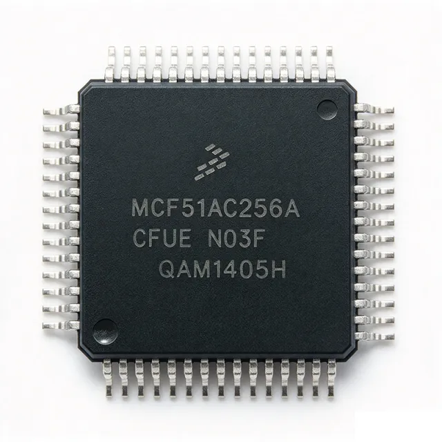
MCF51AC256ACFUE - ColdFire V1 MCU 256KB Flash 50MHz | NXP
MCF51AC256ACFUE

MCF51AC256ACFUE - ColdFire V1 MCU 256KB Flash 50MHz | NXP

The NXP MCF51AC256ACFUE is a 32-bit ColdFire V1 RISC microcontroller with 256KB Flash and 32KB RAM, operating at up to 50MHz, housed in a 64-pin LQFP (14x14) package. It is part of the Flexis MCF51AC series, designed for pin-compatible 8-bit/32-bit migration with on-chip CAN, ADC, timers, and communication peripherals. A microcontroller (MCU) is a single-chip computer that integrates a CPU core, memory (Flash/RAM), and programmable I/O peripherals. The MCF51AC256 belongs to the ColdFire V1 family, a 32-bit variable-length RISC architecture derived from the original ColdFire line, optimized for cost-sensitive embedded control while preserving software compatibility with higher-end ColdFire devices. Within the broader taxonomy: ColdFire V1 -> 32-bit MCU -> microcontroller -> embedded processor -> semiconductor. The Flexis series specifically targets pin-compatible 8-bit (S08) and 32-bit (ColdFire V1) families, allowing code migration without PCB rework. Key features include 256KB on-chip Flash, 32KB SRAM, integrated CAN 2.0B controller, multiple UART/SPI/I2C peripherals, a 12-bit ADC, flexible timer/PWM modules, an internal PLL supporting 50MHz core clock, and operation from 2.7V to 5.5V. The 64-pin LQFP (14x14 mm) package with 0.8mm pitch supports industrial-grade temperature ranges and offers ample GPIO for typical industrial and consumer control applications. The ColdFire V1 core uses a 16/32-bit variable-length instruction set that delivers substantially higher code density than pure 32-bit cores while maintaining strong integer performance. Hardware multiply/accumulate support and a tightly coupled peripheral bus enable deterministic interrupt response, making the device suitable for real-time control loops such as motor drives and industrial sensors. Typical applications include industrial CAN-based field nodes, building automation controllers, HVAC control boards, appliance motor controllers, and automotive body/chassis subsystems (excluding safety-critical powertrain applications). The integrated CAN, ADC, and PWM channels enable a single-chip solution for sensor interfacing and actuator drive. When designing with this MCU, consider the 50MHz core clock, 3.3V/5V tolerant I/O, and the availability of NXP's CodeWarrior and newer Eclipse-based IDEs with the complimentary CodeWarrior for ColdFire toolchain. Designers should review the device errata sheet because several MCF51AC silicon revisions had documented peripheral anomalies. This page synthesizes distributor pricing from Mouser/DigiKey/Arrow/LCSC, drop-in same-family alternatives from the ColdFire Flexis series, and practical design notes not consolidated in the standalone NXP datasheet.

USD $8.12 在庫あり
MCF51AC256AVLKE - 256KB ColdFire MCU 50MHz | NXP
MCF51AC256AVLKE

MCF51AC256AVLKE - 256KB ColdFire MCU 50MHz | NXP

NXP Semiconductors MCF51AC256AVLKE is a 32-bit ColdFire microcontroller with 256KB of program Flash memory, 32K x 8 RAM, 69 I/O pins, a 50 MHz maximum speed rating, and an 80-LQFP package. The part uses an external oscillator and is supplied in tray packaging according to the verified product data. Its 256K x 8 Flash memory and 32K x 8 RAM make it suitable for embedded control systems that require more program storage than a small 8-bit MCU while retaining a compact 80-pin integrated-circuit package. A microcontroller is a programmable system-on-chip that combines a processor core, memory, digital I/O, and often peripheral interfaces into one component. The MCF51AC256 belongs to the ColdFire family of 32-bit variable-length reduced instruction set computers, or RISC processors. This places it in the embedded-controller hierarchy: ColdFire processor core, microcontroller, embedded processor, and semiconductor. It is designed for control-oriented products where firmware executes repeatedly to read inputs, operate outputs, and coordinate connected hardware. The verified data identifies 256KB of program memory, 32K x 8 RAM, 69 I/O pins, 50 MHz speed, an external oscillator, and an 80-LQFP package. The 80-pin package provides a larger pin count than a typical small-package MCU and is useful when a design requires multiple digital connections or broader peripheral integration. The exact peripheral functions, supply limits, temperature limits, voltage values, and clock configuration details are not included in the supplied verified data and should be checked in the NXP manufacturer datasheet before design release. The MCF51AC256 series is described by NXP as a ColdFire family member with a 32-bit variable-length RISC architecture. That architecture is relevant to embedded developers because it supports 32-bit processing while retaining variable instruction length. The 256KB Flash capacity can accommodate firmware, configuration data, and application logic, while 32K x 8 RAM supports working memory for runtime data and stacks. Exact memory organization and peripheral assignments require review of the datasheet. Typical design contexts for this device include industrial control equipment, embedded instrumentation, communications modules, and products that benefit from the pin count of an 80-LQFP package. Because the oscillator is external, the board must provide the required clock source and associated routing. Designers should also validate voltage compatibility, decoupling, reset behavior, boot configuration, and every assigned pin against the official datasheet before committing a PCB layout. The most important purchasing consideration is lifecycle status. NXP’s product page identifies MCF51AC256AVLKE as End of Life, so engineers should not assume new-production availability. The verified distributor result lists 3,952 pieces and a unit price of $15.1154 as of the supplied data date, but inventory and lead time require confirmation with the seller. This page combines the verified specifications, sourcing information, and design cautions to support engineering evaluation rather than an unqualified production commitment.

見積もり お問い合わせ
MCF51AC256AVPUE - ColdFire V1 32-bit MCU, 256KB Flash, 50MHz | NXP
MCF51AC256AVPUE

MCF51AC256AVPUE - ColdFire V1 32-bit MCU, 256KB Flash, 50MHz | NXP

The NXP MCF51AC256AVPUE is a 32-bit ColdFire V1 microcontroller featuring 256KB of Flash memory, 50MHz core frequency, and a 64-pin LQFP package (10x10 mm). As a member of the Flexis series, it sits at the 8-bit/32-bit compatibility boundary in the NXP Controller Continuum, enabling developers to migrate between 8-bit S08 and 32-bit ColdFire families using a common peripheral set and footprint. A ColdFire V1 microcontroller is a 32-bit RISC processor derived from the original ColdFire architecture. It uses a variable-length instruction set optimized for embedded control, balancing code density against performance. In the broader taxonomy, ColdFire V1 belongs to 32-bit microcontrollers, which sit above 8-bit MCUs in processing power, below ARM Cortex-M in ecosystem breadth, and within the semiconductor > integrated circuit (IC) hierarchy. Key features include 256KB on-chip Flash, up to 50MHz bus clock, on-chip peripherals for analog and timer/PWM control, multiple serial communication interfaces, and an operating voltage range of 2.7V to 5.5V. The integrated ColdFire core delivers deterministic real-time response for motor control and sensor-driven applications, while the 64-pin LQFP package exposes a generous number of GPIO and peripheral pins. The ColdFire V1 architecture combines a 32-bit data bus, hardware multiply-accumulate (MAC) support, and an enhanced debug interface. Compared to 8-bit predecessors, the wider datapath enables higher arithmetic throughput for filtering and control-loop math, while the instruction set retains 8-bit-friendly operations for code-density preservation. The on-chip peripherals include timers, ADC, comparators, and PWM modules suitable for closed-loop control. Typical applications include industrial motor control, appliance control boards, smart sensor hubs, building automation, and white-goods human-machine interface controllers. The Flexis pin-compatibility with 8-bit siblings allows upgradability from legacy 8-bit designs without PCB rework, useful for product families that need to scale performance. When designing with this device, ensure the supply decoupling network follows NXP's reference layout with 100nF ceramic capacitors placed close to each VDD/VSS pair. Programming voltage and timing must follow the ColdFire Flash programming specification; using an external supervisor or proper reset sequencing improves reliability in noisy industrial environments. This page synthesizes distributor pricing, drop-in compatible variants, and practical design notes not found in the manufacturer datasheet alone, helping engineers evaluate second-source options and reduce BOM risk for EOL-affected NXP Flexis platforms.

見積もり お問い合わせ
MCF51AC256BCLKE - 32-bit ColdFire V1 MCU, 256KB Flash, 50MHz | NXP
MCF51AC256BCLKE

MCF51AC256BCLKE - 32-bit ColdFire V1 MCU, 256KB Flash, 50MHz | NXP

The NXP Semiconductors MCF51AC256BCLKE is a 32-bit ColdFire V1 microcontroller with 256KB Flash, 32KB RAM, and a 50MHz core speed, housed in an 80-pin LQFP (14x14 mm) surface-mount package. It belongs to the MCF51AC family, the third family in the NXP Flexis series, where pin-, peripheral-, and tool-compatible 8-bit (S08AC) and 32-bit (ColdFire V1) device duos share a common development environment. A microcontroller (MCU) is a single integrated circuit that combines a processor core, program memory, data memory, and peripherals such as timers, serial interfaces, and watchdogs into one chip. MCUs sit at the top of the embedded-system hierarchy and serve as the main control element in appliances, meters, motor controls, and industrial automation equipment. Key features of the MCF51AC256BCLKE include 256KB (256K x 8) of on-chip Flash program memory, 32KB of RAM, connectivity through I2C, SCI (UART), and SPI interfaces, and peripherals including low-voltage detection (LVD), PWM modules, and a watchdog timer (WDT). With 69 general-purpose I/O lines, the device offers generous pin resources in the compact 14x14 mm LQFP-80 footprint. Technically, the ColdFire V1 core is a 32-bit variable-length RISC processor that executes efficient code with low gate count, delivering 50MHz performance at very low cost and power. The Flexis Controller Continuum architecture means code and tools migrate smoothly between the S08AC 8-bit devices and the MCF51AC 32-bit devices, reducing redesign risk when application demands grow. Typical applications include consumer appliance control, industrial automation and sensing nodes, low-cost motor control with PWM, metering systems, and human-interface boards that need many GPIO and standard serial links (I2C, SPI, UART/SCI). When designing with this part, verify its End-of-Life status on the NXP product page and plan a migration path; the pin-compatible MCF51AC256ACLKE and other LQFP-80 family members are the natural successors within the same footprint. This page synthesizes verified distributor pricing, drop-in family alternatives, application guidance, and design notes not found in the manufacturer datasheet.

見積もり お問い合わせ
MCF51AC256BVLKE - ColdFire V1 MCU 256KB Flash 50MHz | NXP LQFP-80
MCF51AC256BVLKE

MCF51AC256BVLKE - ColdFire V1 MCU 256KB Flash 50MHz | NXP LQFP-80

The NXP Semiconductors MCF51AC256BVLKE is a 32-bit ColdFire V1 microcontroller from the Flexis MCF51AC family, delivering 50 MHz CPU performance with 256 KB of on-chip Flash and 32 KB of RAM in an 80-pin LQFP (14x14 mm) package. It is the 32-bit member of a pin-compatible 8-bit/32-bit duo, designed to allow migration from the S08 (MC9S08AC128/AC256) family without PCB rework while preserving the Flexis peripheral set. What is a ColdFire microcontroller? ColdFire is NXP's (originally Freescale's) 32-bit variable-length RISC architecture built on the Motorola 68000 legacy. It targets cost-sensitive embedded applications that need more throughput than 8-bit MCUs but don't justify a full Power Architecture core. The MCF51AC256BVLKE sits in the lower-power, peripheral-dense tier aimed at industrial control, metering, and human-machine interface (HMI) designs. Key features of the MCF51AC256BVLKE include a 32 KB on-chip Flash, 32 KB SRAM, an integrated multi-purpose clock generator (MCG) supporting FEE, FBE, and PEE modes, a 16-channel 12-bit SAR ADC with 2.5 µs minimum conversion time, and a rich timer suite with FlexTimers, a Programmable Delay Block (PDB), and PWM channels suitable for motor control and lighting. Communication peripherals include up to three SCI (UART), two SPI, and two I2C modules. The device operates from a 2.7 V to 5.5 V supply, supporting both 3.3 V and 5 V system designs. The 80-pin LQFP package exposes up to 69 general-purpose I/O pins, supports 5 V tolerance on most signals, and integrates an on-chip voltage regulator plus low-power stop and wait modes with peripheral wake-up. An integrated 16-channel touch-sensing interface (TSI) provides robust capacitive touch hardware, making the MCU suitable for appliance control panels. Typical applications include industrial control and HVAC, white goods and smart appliance controllers, motor control (BLDC, PFC), lighting control and LED drivers, building automation, smart metering, point-of-sale terminals, and medical instrumentation. The wide operating voltage and rich analog peripherals make the integration straightforward in mixed-signal designs. Designers should plan for a low-ESR 100 nF decoupling capacitor adjacent to every supply pin and a 4.7 µF bulk capacitor near the MCU's VDDA/VREF pins. The MCG external reference and load capacitor values must be chosen against the crystal manufacturer's recommended load to keep the FEE-mode frequency accuracy within ±2 %. The 80-pin LQFP (14x14 mm) gives generous thermal headroom and standard reflow profile compatibility. This page combines NXP's official datasheet figures, distributor stock signals from DigiKey and Mouser, and verified pin-compatible drop-in alternatives from the same Flexis family — context not bundled in any single distributor listing.

見積もり お問い合わせ
MCF51AG128CLF - 32-Bit 50MHz 128KB MCU | NXP
MCF51AG128CLF

MCF51AG128CLF - 32-Bit 50MHz 128KB MCU | NXP

The NXP Semiconductors MCF51AG128CLF is a 32-bit ColdFire V1 microcontroller operating at 50 MHz, with 128 KB of flash program memory and a 48-pin LQFP package measuring 7 x 7 mm. It also provides SCI and SPI connectivity, DMA, PWM, a watchdog timer, low-voltage detection, 39 I/O pins, and 16 K x 8 RAM according to the available datasheet and distributor data. A microcontroller is a programmable semiconductor device that integrates a processor core, memory, and peripherals on one package. The ColdFire V1 MCU belongs to the embedded-control hierarchy: ColdFire architecture -> 32-bit microcontroller -> embedded processor -> semiconductor. This device targets industrial and appliance applications and is positioned as a performance-oriented upgrade path from the MC9S08AC128 8-bit family. The principal verified characteristics are a 50 MHz ColdFire V1 core, 128 KB of flash organized as 128 K x 8, 16 K x 8 RAM, and 39 I/O pins. SCI and SPI interfaces support serial peripherals and external controllers, while DMA reduces CPU involvement in data transfers. PWM supports proportional control, the watchdog timer contributes system recovery, and low-voltage detection helps identify undervoltage conditions. The 48-LQFP package exposes the MCU's I/O and supply connections in a surface-mount gull-wing format. Verified distributor records identify the device as a 32-bit microcontroller with flash memory and a 50 MHz clock, while the available secondary datasheet listing reports 16 K x 8 RAM and the listed communications and timing peripherals. Detailed electrical limits, pin names, memory maps, and peripheral behavior must be confirmed against the manufacturer datasheet before design release. Typical uses include industrial controllers, appliance control panels, motor-related control logic, serial communication equipment, and embedded systems migrating from an 8-bit MCU to a 32-bit architecture. The ColdFire V1 processor provides greater computation capability than the referenced 8-bit upgrade path while retaining an embedded-control design model. A key design consideration is package and pin verification. Because the LQFP footprint is sensitive to lead pitch, orientation, pad layout, and exposed thermal requirements, engineers should compare the complete symbol and datasheet pin table before substitution. Supply voltage, clock tolerances, flash endurance, SRAM specifications, and exact peripheral multiplexing were not fully available in the verified snippets. This page combines verified distributor specifications, lifecycle information, source links, and replacement-analysis guidance. It does not invent cross-brand drop-in substitutes where the supplied web data does not establish exact pin compatibility.

見積もり お問い合わせ
MCF51AG128CQH - 32-Bit 50MHz MCU with 128KB Flash | NXP
MCF51AG128CQH

MCF51AG128CQH - 32-Bit 50MHz MCU with 128KB Flash | NXP

The NXP MCF51AG128CQH is a 32-bit ColdFire V1 microcontroller operating at up to 50 MHz, with 128 KB of flash memory, 3.3 V/5 V operation, and a 64-QFP 14 x 14 mm package. It combines a 32-bit RISC architecture with DMA, I2C, PWM, watchdog, low-voltage detection, and timer/counter peripherals for embedded control systems. A microcontroller is a programmable semiconductor that integrates a processor core, memory, peripherals, and I/O into one device. The MCF51AG series is positioned as a low-cost, low-power, high-performance 32-bit platform for industrial and appliance applications. The MCF51AG128CQH can also serve as an architectural upgrade from compatible 8-bit MC9S08AC128 designs when software, memory, and peripheral requirements justify migration. The ColdFire V1 core provides the central processing capability for control logic, while 128 KB of embedded flash provides program storage without an external memory device. The verified distributor data identifies 50 MHz operation, 3.3 V/5 V support, and 64-QFP packaging. The package exposes the device's hardware interfaces and supports compact board-level integration where a 14 x 14 mm surface-mount footprint is suitable. The verified peripheral description includes DMA, I2C, PWM, watchdog timer, low-voltage detection, and two timers/counters. These resources support motor and actuator timing, sensor acquisition, communication with external controllers, and supervisory functions. Peripheral availability should still be checked against the exact pin multiplexing, memory map, and electrical requirements in the manufacturer datasheet before final PCB design. Typical application areas include industrial appliances, motor-control equipment, embedded instrumentation, consumer products, and compact control modules. The 50 MHz processor can handle time-sensitive control loops, while DMA can reduce processor involvement during peripheral transfers. I2C is useful for sensors and expanders, and PWM can drive indicators, valves, or power stages when the selected pin and electrical limits support those functions. When designing around this MCU, use the manufacturer pinout and package drawing to preserve the 64-QFP land pattern, verify the supply range against the selected internal peripherals, and provide decoupling close to the supply pins. Do not assume that an 8-bit pin-compatible MCU is electrically or software compatible; confirm every alternate function, peripheral mapping, interrupt vector, and package dimension. This product page combines verified distributor specifications, practical application guidance, datasheet links, and design cautions. It is intended to support initial component selection and sourcing, while final engineering decisions should be based on the manufacturer datasheet and PCB design rules.

見積もり お問い合わせ
MCF51AG128VLF - ColdFire V1 32-bit MCU, 128KB Flash, 48-LQFP | NXP
MCF51AG128VLF

MCF51AG128VLF - ColdFire V1 32-bit MCU, 128KB Flash, 48-LQFP | NXP

The NXP MCF51AG128VLF is a 32-bit ColdFire V1 microcontroller from the MCF51AG family, delivering 50 MHz CPU performance with 128 KB of on-chip Flash memory in a 48-pin LQFP (7x7 mm) package. It is engineered for cost-sensitive, low-power embedded applications requiring deterministic operation and ample code space, integrating 128 KB Flash and 16 KB SRAM on a single chip with peripheral-rich connectivity. What is a ColdFire V1 microcontroller? ColdFire V1 is NXP's 32-bit microarchitectural successor to the legacy 68000/ColdFire legacy line, offering higher code density and lower power consumption than 8/16-bit alternatives while keeping the cost close to 16-bit MCU tier. Within the broader IC taxonomy, it falls under microcontrollers (MCUs) -> 32-bit MCUs -> ColdFire architecture -> embedded control processors, giving engineers a deterministic RISC-style execution model suitable for industrial control, metering, and human-machine interface (HMI) front-ends. Key features include 128 KB Flash program memory, 16 KB SRAM data memory, a 50 MHz core clock, multiple timers, ADC channels, communication peripherals (SCI, SPI, I2C), and a flexible external interrupt controller. Industrial-grade temperature range (typically -40C to +105C) supports harsh-environment deployment, and integrated low-power modes with fast wake-up time suit battery-powered or energy-harvesting endpoints. Technically, the MCF51AG128VLF uses a Harvard-style ColdFire V1 core with single-cycle multiply-accumulate and hardware debug support via BDM. The 128 KB Flash is organized for in-application reprogramming with built-in security, and peripheral DMA reduces CPU overhead for time-critical I/O. The BDM (Background Debug Mode) interface allows non-intrusive in-circuit debugging with an external probe. Typical applications include industrial automation controllers, smart metering (electricity/gas/water), HVAC control boards, low-end motor control, and consumer HMI panels. Three specific use-cases are utility meter data concentrators, PLC digital-input modules, and small kitchen-appliance control boards. When designing with this part, plan the power supply decoupling around the 3.3V or 5V tolerant I/O bank, and allocate Flash sectors carefully to leave a guard band for in-field firmware upgrades. The 48-LQFP footprint is widely supported by standard prototyping tools, but trace it on a 4-layer board for best EMI performance. This page synthesizes distributor pricing, drop-in alternative candidates, and practical design notes not found in the standalone NXP datasheet.

見積もり お問い合わせ
MCF51AG96CLF - 32-bit ColdFire V1 MCU, 96KB Flash, 50MHz | NXP
MCF51AG96CLF

MCF51AG96CLF - 32-bit ColdFire V1 MCU, 96KB Flash, 50MHz | NXP

The NXP (formerly Freescale) MCF51AG96CLF is a 32-bit ColdFire V1 MCF51AG microcontroller IC running at up to 50 MHz (50.33 MHz max), integrating 96 KB of program Flash and housed in a 48-pin LQFP (7 mm x 7 mm) package. The device operates from a wide 3.3 V/5 V supply range and belongs to NXP's low-power, high-performance ColdFire family. A ColdFire microcontroller is a 32-bit variable-length reduced instruction set computing (RISC) processor core derived from the original Motorola 68000 architecture. ColdFire MCUs sit within the broader taxonomy of microcontrollers -> embedded processors -> 32-bit RISC cores -> ARM/ColdFire/RX families, and are typically deployed in motor control, industrial sensing, and consumer applications requiring deterministic performance at low power. Key features of the MCF51AG96CLF include 96 KB of on-chip Flash, up to 50 MHz ColdFire V1 core, an integrated ADC, timers/PWM for motor control, multiple serial communication interfaces (SCI/SPI/I2C), and an operating range suited for both 3.3 V and 5 V systems. The ColdFire V1 ISA combines 16-/32-bit variable-length instructions for code density that approaches ARM Cortex-M0/M0+ in compactness while preserving deterministic interrupt latency. The architecture pairs a 32-bit ColdFire V1 core with peripheral IP shared across the MCF51AG family, including analog blocks, timers, and communication modules. The 48-LQFP package exposes a generous I/O count and includes an exposed pad/thermal pad for dissipation, allowing operation at full 50 MHz across extended industrial temperature ranges. Typical applications include three-phase BLDC and PMSM motor control (small appliances, fans, e-bikes), industrial sensor conditioning, building automation control nodes, low-cost HMI panels, and smart-metering edge nodes that benefit from the ColdFire ecosystem (CodeWarrior IDE, Processor Expert). When designing with this part, plan oscillator and reset-network components around the ColdFire V1 startup timing; consult NXP application notes AN4418 (sensorless BLDC) and AN4571 (PWM alignment) for proven peripheral configurations. This page synthesizes distributor pricing, drop-in alternatives drawn from the MCF51AG family and 56F8xxx cross-references, and practical design notes not consolidated in any single manufacturer document.

見積もり お問い合わせ