製品 (39,000+)

MCZ33884EGR2 - 24-SOIC Switch Monitor Interface | NXP
MCZ33884EGR2

MCZ33884EGR2 - 24-SOIC Switch Monitor Interface | NXP

The NXP MCZ33884EGR2 is a monolithic switch monitor interface IC housed in a 24-pin SOIC (0.295 inch / 7.50 mm width) package and shipped on Tape & Reel. According to the NXP datasheet, the 33884 device performs switch monitoring functions and provides efficient interface between electrical switches and a microcontroller domain, commonly used in automotive body and chassis electronic control units. A switch monitor interface (also called a switch contact monitor or contact sense interface) is a mixed-signal IC that conditions, debounces, and digitizes the state of mechanical or semiconductor switches before passing the result to an MCU. It sits in the system hierarchy between raw electromechanical inputs (door switches, ignition, brake pedals, seat-occupancy sensors) and the microcontroller GPIO/ADC inputs, and is itself a sub-category of specialized interface ICs within the broader Interface IC > Specialized > Automotive Switch Monitor family. Key features of the MCZ33884EGR2 include monitoring of multiple switch inputs against programmable thresholds, programmable wetting current for the contact supply, integrated debounce logic, and diagnostic feedback for open/short detection. The 24-SOIC package gives 24 I/O channels, sufficient for body controllers supervising door, trunk, hood, ignition-key, and seat-belt switch matrices. The interface operates directly from the vehicle 12 V supply domain and produces logic-level outputs compatible with 3.3 V or 5 V MCUs. Internally, the device uses bipolar analog front ends for wetting-current regulation and CMOS logic for state decoding, with on-chip timing for debounce windows. The monolithic integration eliminates external comparators, pull-up resistors, and discrete debounce RC networks, reducing PCB area and improving reliability under automotive temperature and EMI stress. Typical applications include automotive body controllers, door/window/seat switch matrices, electronic steering column locks, ignition switch supervisors, and industrial PLC digital input modules. In each case the IC translates a contact-closure event into a clean, debounced logic state for the host processor. Design consideration: when laying out the PCB, keep the high-current wetting-current traces short and place a 100 nF decoupling capacitor directly at the VCC pin. The wetting current itself is programmable via an external resistor and must be sized per switch contact material (typical 1-10 mA) to prevent oxidation while staying within EMI limits. This page synthesizes distributor pricing, drop-in same-footprint alternatives, and practical switch-monitor design notes not contained in the NXP datasheet alone.

見積もり お問い合わせ
MCZ33889BEG - SBC-Lite LS-CAN System Basis Chip | NXP
MCZ33889BEG

MCZ33889BEG - SBC-Lite LS-CAN System Basis Chip | NXP

The NXP MCZ33889BEG is a System Basis Chip (SBC-Lite) with a low-speed fault-tolerant CAN interface, housed in a 28-pin SOIC (7.50 mm) wide-body package. It integrates a 5V linear regulator, a low-speed CAN physical layer compliant with ISO 1186-3, watchdog, reset, and SPI-configurable diagnostics into a single monolithic device aimed at automotive body and powertrain ECUs. A System Basis Chip (SBC) is an integrated mixed-signal IC that consolidates multiple functions repeatedly required in microcontroller-based designs—power supply, communication transceivers, diagnostics, and protection—onto a single die. An SBC sits between the battery/12V bus and the MCU on a node, replacing what used to be a discrete LDO, CAN transceiver, and supervisor. Compared with using separate components, an SBC reduces PCB area, BOM count, and design complexity while improving reliability through unified fault handling. Key features of the MCZ33889BEG include: a 5V/350 mA on-board voltage regulator for the microcontroller supply rail; a low-speed CAN transceiver supporting ISO 11898-3 (fault-tolerant up to 125 kbps) for body-electronics networks; a windowed watchdog and reset circuit for microcontroller supervision; SPI interface for configuration and diagnostics; and integrated protection such as thermal shutdown, short-circuit limiting, and battery reverse-polarity handling. The architecture combines a bipolar power section for high-voltage transients on the CAN bus with CMOS logic for the digital control interface. The fault-tolerant CAN bus remains functional in the presence of certain wiring faults (open/short to ground/VBAT) through active bus biasing and fault detection per ISO 11898-3. Typical applications include automotive body control modules (BCM), HVAC modules, instrument clusters, seat and door modules, gateway ECUs, and any in-vehicle network node requiring a regulated 5V rail and a fault-tolerant low-speed CAN interface on the same chip. When designing with the MCZ33889BEG, ensure adequate thermal copper on the SOIC-28 EP pad and verify the load current on VDD5 (3A peak transient handling is not specified—observe the 350 mA continuous rating). Decoupling capacitors on VDD5 and the CAN bus lines should follow NXP's reference layout. This page consolidates distributor pricing, drop-in alternatives, and design notes synthesized from the manufacturer datasheet and cross-reference data—information gain not found in the manufacturer datasheet alone.

見積もり お問い合わせ
MCZ33903BD5EK - SBC Gen2 CAN HS/LIN 32-SOIC EP | NXP
MCZ33903BD5EK

MCZ33903BD5EK - SBC Gen2 CAN HS/LIN 32-SOIC EP | NXP

The NXP (formerly Freescale) MCZ33903BD5EK is a second-generation System Basis Chip (SBC) that integrates a high-speed CAN transceiver, a LIN transceiver, a 5.0 V/100 mA low-dropout voltage regulator, and a window watchdog in a 32-pin SOIC Wide Body with Exposed Pad (SOIC-32 EP, 7.50 mm body width) package. It operates over a wide 5.5 V to 28 V supply range (load-dump tolerant) and is targeted at automotive in-vehicle networking where body controllers, HVAC modules, seat controllers and door modules must combine bus communications with a regulated logic supply. A System Basis Chip (SBC) is a category of multi-function automotive IC that combines several discrete blocks - typically a CAN/LIN physical layer transceiver, a 5 V or 3.3 V LDO regulator, a watchdog timer, and fault/safety outputs - into one monolithic device. Within the broader taxonomy, an SBC sits at the boundary between an interface IC (CAN/LIN PHY) and a power management IC (the on-board LDO), and is commonly counted as a network/interface IC. The 33903 family is the second-generation successor to the original 3390x SBCs and improves on the first generation with a wider supply range, improved EMC behavior and selectable bus-interface modes. Key features of the MCZ33903BD5EK include: high-speed CAN compliant with ISO 11898-5, LIN 2.x compliant with the LIN physical layer, an internal 5.0 V LDO rated for up to 100 mA load, a selectable normal/sleep operating mode for quiescent-current-sensitive modules, an integrated window watchdog for host-microcontroller supervision, and a fault-output pin for system-level diagnostics. The device supports wake-up via CAN or LIN traffic. Supply voltage is specified to withstand automotive transient conditions including jump-start and load-dump events. Architecturally, the IC combines a high-speed CAN transceiver core (with split termination control, slope/rate selection, and a TXD dominant time-out safeguard), a LIN 2.0/2.1/2.2-compliant transceiver, and a low-quiescent 5 V linear regulator. Internal logic is driven from the regulated 5 V rail so that bus interfacing stays galvanically referenced to V_sup through the on-chip linear regulator stage, simplifying external component count. The exposed pad is electrically tied to the IC substrate ground and must be soldered to the PCB ground pour for both thermal and EMC performance. Typical applications include automotive body-domain modules such as HVAC control units, power seat controllers, door modules, lighting controllers, instrument-cluster accessory rails, and gateway nodes bridging CAN and LIN subnets. Designers choose the 33903 because it collapses what would otherwise be a discrete 5 V LDO, a CAN transceiver, a LIN transceiver, and a watchdog supervisor into one AEC-Q100-qualified part. Design consideration: the SOIC-32 EP exposed pad must be soldered to a sufficient copper area to handle the internal 5 V LDO dissipation. With a 12 V automotive supply and a 100 mA load, the LDO drops 7 V and dissipates approximately 0.7 W; without the exposed-pad land pattern the junction temperature can exceed the 150C automotive limit. This page synthesizes multi-source distributor pricing, same-package drop-in alternatives, and practical design notes not collected in any single manufacturer document.

見積もり お問い合わせ
MCZ33903BS5EKR2 - SBC Gen2 w/ HS CAN & LIN | NXP | 32-SSOP-EP
MCZ33903BS5EKR2

MCZ33903BS5EKR2 - SBC Gen2 w/ HS CAN & LIN | NXP | 32-SSOP-EP

The NXP MCZ33903BS5EKR2 is a System Basis Chip (SBC) Gen2 with High-Speed CAN and LIN interface, housed in a 32-pin SSOP-EP (exposed pad) package. It integrates a 5V/100mA voltage regulator, a high-speed CAN transceiver compliant with ISO 11898-5, a LIN 2.1 transceiver, four wake inputs, and a fail-safe SPI control interface in a single IC. Operating from a 5.5V to 27V supply (with load-dump tolerance to 40V), it targets 12V automotive body and chassis networks. A System Basis Chip (SBC) is an automotive power-supply and communication IC that combines a voltage regulator, bus transceivers (CAN/LIN), and digital control logic into one package. In the broader component hierarchy it sits between a discrete transceiver + LDO combination and a full automotive microcontroller, reducing PCB area and BOM count in body control modules, gateways, and sensor clusters. Key features of the MCZ33903BS5EKR2 include AEC-Q100 Grade 1 qualification (-40C to +125C), integrated HS-CAN transceiver supporting 1 Mb/s, LIN 2.1 transceiver with internal pull-up, four wake-input pins for low-power standby modes, watchdog timer, and an SPI-controlled diagnostic/mode register. The 32-SSOP-EP exposed pad provides ~28 C/W thermal resistance, sufficient for the ~300mW typical dissipation. Architecturally, the device uses a switched-mode or linear 5V pre-regulator (the data summary indicates 'HS 5V') feeding an internal LDO for logic, while a charge pump supplies the CAN bus driver for true dominant-output symmetry. The LIN channel uses an internal slope control for low-EMI operation. Typical applications include automotive body control modules, HVAC controllers, seat/window/liftgate modules, steering-angle sensor interfaces, lighting ECUs, and CAN/LIN gateway nodes. Its 27V load-dump tolerance makes it suited to directly connected 12V battery rails. A critical design tip: the exposed pad must be soldered to a ground plane for thermal dissipation and ESD performance. Use 100nF X7R bypass close to VCC and follow NXP's AN4760 layout guidance for CAN bus impedance control (60 ohm differential, 120 ohm termination at each bus end). This page synthesizes distributor pricing, AEC-Q100 context, and pin-compatible same-family alternatives that go beyond the manufacturer datasheet, providing a single sourcing and selection reference for automotive hardware engineers.

見積もり お問い合わせ
MCZ33903CP3EK - SBC CAN HS 3.3V + LIN | NXP Semiconductors
MCZ33903CP3EK

MCZ33903CP3EK - SBC CAN HS 3.3V + LIN | NXP Semiconductors

The NXP Semiconductors MCZ33903CP3EK is a second-generation System Basis Chip (SBC) integrating a 3.3V voltage regulator, an enhanced high-speed CAN transceiver (ISO 11898-2 and -5), and a LIN bus interface in a single 32-pin SOIC-EP package. Designed as an advanced power management unit for microcontrollers, sensors, and CAN transceivers, it consolidates power, communication, and supervisory functions that would otherwise require multiple discrete ICs on an automotive ECU. A System Basis Chip (SBC) is a highly integrated mixed-signal IC that combines a voltage regulator, communication transceivers, and watchdog/safety logic in one package. The SBC belongs to the power management IC family, sits hierarchically above simple LDOs and DC-DC converters, and serves as the power-and-communication backbone of an automotive electronic control unit (ECU). It bridges the harsh 12V/24V automotive bus to clean logic-level rails and fieldbus networks. Key features of the MCZ33903CP3EK include a selectable 5.0V or 3.3V MCU voltage regulator with current capability extendable via an external PNP pass transistor, embedded CAN transceiver offering local and bus-failure diagnostics, voltage/current/temperature protection, and extremely low quiescent current in sleep and standby modes. The device also integrates LIN, ISO 9141, and a window watchdog for MCU safety. The architecture combines an analog LDO controller with two independent physical-layer transceivers. The high-speed CAN transceiver meets ISO 11898-2 and -5 with ±8 kV ESD on the bus pins, while the LIN transceiver is LIN 2.0/2.1 compliant. Internal state machines manage power modes, fault reporting, and fail-safe behavior, eliminating firmware overhead for basic bus diagnostics. Voltage, current, and thermal protection circuits guard against load-dump transients and short-circuit conditions common in automotive environments. Typical applications include automotive body controllers, gateway modules, door/lighting/HVAC ECUs, and industrial CAN nodes. The integrated 3.3V/5V regulator supplies the host MCU directly, while the CAN/LIN transceivers connect to vehicle bus networks. AEC-Q100 qualification makes it suitable for under-hood and passenger-compartment deployments. When designing with the MCZ33903CP3EK, follow NXP's reference layout in the datasheet and respect thermal limits - the exposed pad must be soldered to a sufficient copper area. Note that the base MPN is end-of-life; pin-compatible drop-in alternatives within the MC33903 family are recommended for new designs. This page synthesizes distributor pricing, drop-in alternatives within the MC33903 family, and practical design notes not found in the manufacturer datasheet.

見積もり お問い合わせ
MCZ33904C3EKR2 - SBC, 2x 3.3V/400mA LDO, HS CAN, 32-SOIC-EP | NXP
MCZ33904C3EKR2

MCZ33904C3EKR2 - SBC, 2x 3.3V/400mA LDO, HS CAN, 32-SOIC-EP | NXP

The NXP MCZ33904C3EKR2 is a second-generation System Basis Chip (SBC) integrating two 3.3 V/400 mA LDO regulators, a high-speed CAN transceiver compliant with ISO 11898-2 and ISO 11898-5, four wake-up inputs, and advanced fault diagnostics, all housed in a 32-pin SOIC-EP (exposed pad) package supplied on tape and reel. The MCZ33904 family operates from a 5.5 V to 28 V supply rail, supporting 12 V and 24 V automotive bus systems while offering Normal, Sleep, and Stop power modes optimized for ECU standby current. Two independent 3.3 V LDO regulators (V1 and V2) are capable of delivering up to 400 mA each, providing power to an MCU and companion circuitry such as sensors and CAN transceivers. A System Basis Chip (SBC) is a power management and communication integrated circuit that consolidates multiple discrete functions - typically voltage regulators, a CAN/LIN transceiver, wake-up logic, and supervisory features - into a single device. By integrating these functions, an SBC reduces PCB area, simplifies EMC compliance, and provides deterministic reset and watchdog behavior for automotive ECUs. SBCs sit one level above standalone LDOs and below full PMICs in the automotive power-tree hierarchy, occupying the role of the local ECU supply and bus interface. Key features include enhanced high-speed CAN physical layer with local and bus failure diagnostics, selectable Normal/Sleep/Stop modes for low-Iq standby, configurable window watchdog, and fail-safe operation mode. The 32-SOIC-EP exposed pad reduces thermal resistance and improves reliability in harsh under-hood environments. Built-in protection includes over-temperature shutdown, over-current limiting on each LDO, and bus dominant time-out for the CAN driver. The architecture combines an automotive-grade bipolar/CMOS process, an internal 3.3 V bandgap reference, and low-Iq charge pumps to meet strict OEM quiescent-current budgets (<100 uA in Sleep). The MCZ33904C3EKR2 variant belongs to the 'C3' suffix family, which configures the V2 LDO for 5 V operation or specific ECU power-rail allocations, and the 'EK' indicates the SOIC-EP package option. Typical applications include 12 V automotive body control modules, instrument clusters, gateway ECUs, HVAC controllers, and industrial CAN nodes. The dual 3.3 V rails cleanly power an MCU plus a 5 V-tolerant sensor stage, while the integrated HS-CAN eliminates the need for a standalone transceiver. In Sleep mode the device draws microamp-level quiescent current, supporting always-on wake-up via the WKUP pins for CAN or LIN traffic. When designing with this SBC, place the exposed pad solder stencil to provide at least 50 mm squared of copper to keep junction temperature within range at 28 V worst-case load. Decouple each V1/V2 LDO output with a 1 uF to 10 uF low-ESR ceramic placed within 5 mm of the relevant pin; mis-typed or distant capacitors cause output ripple and regulator instability. This page synthesizes NXP datasheet parameters, distributor stock data from DigiKey and Octopart, and direct drop-in 33904-series alternatives plus 33903/33972 variant comparison points not consolidated in a single manufacturer document.

見積もり お問い合わせ
MCZ33972AEK - Multi-Switch Detection SPI Interface, 8-26V, 32-SOIC-EP | NXP
MCZ33972AEK

MCZ33972AEK - Multi-Switch Detection SPI Interface, 8-26V, 32-SOIC-EP | NXP

The NXP MCZ33972AEK is a multiple switch detection interface with suppressed wake-up, designed to detect the closing and opening of up to 22 switch contacts through an SPI (Serial Peripheral Interface) bus, housed in a 32-pin SOIC-EP (exposed pad) package. It operates over a wide supply voltage range of 8 V to 26 V and integrates a dual H-bridge coil driver with associated control logic, enabling direct stepper motor gauge drive alongside switch monitoring. What is a multiple switch detection interface? This category of mixed-signal interface IC sits between low-current mechanical switches (buttons, door switches, sensor contacts) and a host microcontroller. It replaces dozens of discrete pull-up resistors and input pins by multiplexing the switch states onto an SPI bus, while the suppressed wake-up function prevents the host MCU from being awakened by spurious or bouncing switch events. In the system hierarchy, MCZ33972AEK is a specialized interface IC within the broader power management and body electronics domain. Key features of the MCZ33972AEK include programmable wetting current for each input (typically 2 mA, 6 mA, or 16 mA selectable), built-in switch debounce and over-voltage protection on each input pin, and an ultra-low quiescent current in Sleep mode that makes it ideal for automotive body controllers that must meet stringent quiescent-current budgets during key-off. The exposed pad on the 32-SOIC package reduces thermal resistance and improves reliability under sustained current loads. The device operates in two modes: Normal mode supplies switch contacts with pull-up or pull-down current while continuously monitoring switch state changes for SPI reporting; Sleep mode disables most internal circuitry to draw minimum current until a qualified wake-up event occurs. The wetting current is programmable per channel via SPI, allowing the same IC to interface with both dry contacts and solid-state sensor outputs. Typical applications include automotive body control modules (detecting door, hood and trunk switches), instrument cluster switch matrices, HVAC control panels, and industrial control panels with multiple mechanical inputs. In each case the MCZ33972AEK replaces 22 discrete GPIO channels and their pull-up networks with a single SPI-controlled IC. When designing with this device, calculate worst-case power dissipation from VIN_max and the number of switches simultaneously sourcing wetting current. Place the exposed pad on a minimum 1 square inch copper pour to keep junction temperature within the -40C to +125C automotive operating range. Decouple VCC with a 100 nF ceramic capacitor placed within 5 mm of the supply pin. This page synthesizes distributor pricing, drop-in alternatives, and practical design notes not found in the manufacturer datasheet, including cross-brand substitute guidance and a parameter comparison table for engineers selecting multi-channel switch monitor ICs.

見積もり お問い合わせ
MCZ33972AEKR2 - SPI Switch Detection Interface, 32-SOIC EP | NXP
MCZ33972AEKR2

MCZ33972AEKR2 - SPI Switch Detection Interface, 32-SOIC EP | NXP

The NXP MCZ33972AEKR2 is a multiple switch detection interface with suppressed wake-up, housed in a 32-pin SOIC-EP (exposed pad) package. It communicates over an SPI bus and operates from an 8 V to 26 V supply, making it a direct fit for 12 V and 24 V automotive body and chassis systems. A switch detection interface is a mixed-signal IC that multiplexes multiple mechanical or electronic switch inputs into a single serial data stream for a microcontroller. In the broader system hierarchy it sits below the MCU and above the physical switch network, forming part of the body-electronics domain of automotive electronics. Suppressed wake-up means the device can ignore transient switch events and only assert the wake-up interrupt after a programmed debounce window has passed, reducing false ECU wake-ups. Key features include support for up to 7 direct switch inputs with programmable wetting current, on-chip ESD protection, a low-power standby mode with interrupt wake-up capability, and a 32-bit SPI status register reporting switch state, supply voltage, and fault conditions. The exposed thermal pad on the 32-SOIC package provides a low theta-JA path for dissipating transient load events on the supply pin. From an architectural standpoint the device combines an analog multiplexer, a current source for switch wetting, an analog-to-digital conversion channel for supply monitoring, and a standard SPI slave interface. The same die serves multiple package variants in the 33972 family, allowing PCB reuse across part numbers. The wide 8 V to 26 V analog supply tolerance makes it compatible with cranking transients and load-dump events typical of automotive 12 V rails. Typical applications include automotive body controllers detecting door, hood, and trunk switches, HVAC control panels reading multiple user inputs, and industrial control panels requiring debounced digital inputs over a single SPI bus. The suppressed wake-up feature reduces quiescent current draw by preventing spurious ECU wake-ups from switch bounce or EMI. When designing with this part, place 100 nF decoupling close to VCC and connect the exposed pad to a thermal copper pour of at least 1 square inch to keep junction temperature within SOA during fault conditions. The wake-up timing is set by an external capacitor; consult the manufacturer datasheet for the recommended range. This page synthesizes distributor pricing, drop-in alternatives, and practical design notes not found in the manufacturer datasheet alone, supporting faster sourcing decisions for automotive and industrial switch-interface designs.

見積もり お問い合わせ
MCZ33972AEW - 22-Switch SPI Interface, 8-26V | NXP
MCZ33972AEW

MCZ33972AEW - 22-Switch SPI Interface, 8-26V | NXP

The NXP MCZ33972AEW is a Multiple Switch Detection Interface with Suppressed Wake-up that monitors up to 22 switch contacts in automotive and industrial systems, reporting state through an SPI (Serial Peripheral Interface) to the host MCU. Housed in a 32-SOIC (7.50 mm wide, 0.295 inch body) package, the device operates from an 8 V to 26 V supply range and supports both 3.3 V and 5 V logic families via its VDD logic rail. A switch monitor IC belongs to the broader category of interface ICs and mixed-signal peripherals, sitting between the power-management domain and the digital logic domain in a vehicle or industrial ECU. Multiple switch detection interfaces aggregate wet or dry switch contacts and convert them into a serial stream, freeing up MCU GPIO pins, reducing wiring, and providing deterministic wake-up behavior for body, chassis, and body-control modules. The 33972 family is the de-facto NXP platform for this function, succeeding earlier MC33800/MC33996 scan-only parts by adding programmable wetting current, programmable debounce, and a low-quiescent Sleep mode that enables microamp-level standby currents mandated by modern vehicle parasitic-drain budgets. Key features include: detection of 22 switch inputs, programmable wetting source/sink current on a per-input basis, a 22-to-1 analog multiplexer that can be routed to a dedicated AMUX output pin for ADC measurement, integrated 5 V LDO for VDD logic supply, programmable debounce filter, wake-up capability via a dedicated WK input, two operating modes (Normal and Sleep), and selectable SPI clock polarity/phase. The 32-SOIC wide-body footprint simplifies PCB layout versus smaller 32-QFN variants for hand-rework prototypes. Technically, the device uses a current-source/pull-down architecture for switch detection: each input is biased with a programmable current and the resulting voltage is compared against a threshold. The host MCU programs configuration, threshold, and debounce registers via SPI; switch-change events generate an interrupt on the INTB pin, allowing the MCU to enter Sleep between interrupts for very low average current. The integrated 22-to-1 AMUX enables precise analog measurement of each switch pin via the host ADC, supporting diagnostics for stuck-open, stuck-shorted, and leakage conditions. Typical applications include automotive body control modules (BCM), steering-wheel switch clusters, HVAC control panels, door modules, seat controllers, and industrial PLC switch and sensor interfaces. The wide 8-26 V supply tolerance covers 12 V and 24 V battery rails directly without pre-regulation. Design with the part by leaving the WK pin accessible for hardware wake-up from Sleep, choosing wetting current per switch type (typically 2-16 mA), and following the NXP recommended layout to keep the SPI traces short and shielded from the switch-input harness. The 32-SOIC wide body simplifies soldering and rework versus QFN but requires slightly more board area; the alternative pin variant MCZ33972AEK uses a 32-SOIC narrow body. This page synthesizes DigiKey and Mouser distributor pricing, drop-in NXP same-family alternatives, and practical design notes not found in the manufacturer datasheet.

見積もり お問い合わせ
MCZ33972EWR2 - 22-Ch Switch Monitor SPI Interface | NXP
MCZ33972EWR2

MCZ33972EWR2 - 22-Ch Switch Monitor SPI Interface | NXP

The NXP MCZ33972EWR2 is a Multiple Switch Detection Interface (MSDI) IC that monitors up to 22 switch contacts and reports their open/closed state to a microcontroller through a 16-bit SPI (Serial Peripheral Interface). Housed in a 32-pin SOIC wide-body package (7.50 mm), it operates from an 8 V to 26 V supply and includes suppressed-wake-up functionality, programmable wetting current, and a 22-to-1 analog multiplexer for sequential switch voltage readout. A Multiple Switch Detection Interface (MSDI) is a type of mixed-signal automotive interface IC that combines analog input multiplexing, programmable current sources, threshold comparators, and a digital serial interface into a single device. In the system hierarchy it belongs to Interface ICs > Specialized Interface ICs, bridging low-level mechanical switches to digital logic. Its primary purpose is to replace dozens of discrete pull-ups, comparators, and wiring with one rugged, AEC-qualified IC, which is critical for body controllers, HVAC panels, and steering-wheel switch clusters. Key features of the MCZ33972EWR2 include detection of 22 switch inputs, a 16-bit SPI output word, user-selectable switch-to-ground or switch-to-battery configuration, programmable wetting current (2 mA / 6 mA / 12 mA / 16 mA typical), and an integrated 22:1 analog MUX output for ratiometric measurement. The wake-up feature pulses a current briefly through each switch on a programmed interval, then returns to a low-Iq Sleep mode, drastically reducing quiescent current in parked-vehicle applications. Normal mode allows continuous monitoring at full speed and full programming access. The device uses an internal 5 V regulator derived from V_PWR to power analog and digital blocks, and provides an interrupt output (INT) to wake the host MCU on any switch state change. The on-chip 22-to-1 analog multiplexer allows a single ADC on the MCU to sequentially read each switch node for ratiometric diagnostics (open circuit, short to battery, short to ground). The architecture is designed to tolerate 40 V load-dump transients common in 12 V automotive networks, with reverse-battery protection on V_PWR. Typical applications include automotive body controllers detecting door, hood, trunk and seatbelt switches, HVAC control panels reading push-buttons and rotary encoders, steering-wheel switch clusters, instrument-cluster switch input, and industrial control panels with multiple contact closures. Its suppressed wake-up and low quiescent current make it well-suited to any battery-powered application where the system must wake on a switch event without continuously drawing power. Designers should note that the 32-SOIC package requires thermal relief and adequate copper for the exposed-pad power-dissipation path, and that the analog MUX output should be buffered if more than a few hundred pF of capacitance is present on the trace. PCB layout must keep the analog MUX trace away from switching power traces to preserve diagnostic accuracy. This page synthesizes NXP datasheet specifications, distributor pricing, drop-in alternatives, and practical design notes not found on the manufacturer product page alone.

見積もり お問い合わせ
MCZ33975EK - 22-Channel Switch Detection SPI Interface | NXP
MCZ33975EK

MCZ33975EK - 22-Channel Switch Detection SPI Interface | NXP

The NXP MCZ33975EK is a 22-channel multiple switch detection interface with suppressed wake-up and 32 mA wetting current, housed in a 32-pin SOIC-EP (Exposed Pad) package. It communicates with a host MCU through an SPI (Serial Peripheral Interface) bus and is qualified to AEC-Q100 automotive standards. A multiple switch detection interface is a specialized analog/digital IC that scans a large array of mechanical or electronic switch contacts and reports their open/closed state to a microcontroller. This category sits within the broader hierarchy of interface ICs -> specialized interfaces -> automotive body electronics drivers. Unlike simple GPIO expanders, switch-detection ICs include programmable wetting current sources, debounce timers, and wake-up suppression logic that allows the rest of the ECU to remain in low-power sleep until a defined switch event occurs. Key features include detection of up to 22 switch contacts, a 5.5 V to 28 V supply range suited to 12 V automotive rails with load-dump margin, 32 mA programmable wetting current per input to prevent oxidation on mechanical contacts, integrated SPI reporting with interrupt capability, and programmable wake-up behavior. The exposed thermal pad on the 32-SOIC-EP package reduces junction-to-ambient thermal resistance, allowing sustained operation at full wetting-current load across all 22 channels. The device is built on a high-voltage BCD (Bipolar-CMOS-DMOS) process that supports direct connection to automotive battery nodes without external level shifting. Each of the 22 input channels integrates a wetting-current source, comparator, and debounce state machine. The suppressed wake-up feature allows the IC to ignore brief or noisy switch events and only interrupt the MCU when a genuine, sustained contact transition occurs, dramatically reducing ECU sleep-mode current in body-comfort applications. Typical applications include automotive body control modules reading door, hood, and trunk ajar switches, climate-control panel buttons, seat-occupancy and buckle switches, lighting controls, and any distributed switch matrix that must communicate over SPI to an MCU. The wide supply range also supports industrial 24 V control panels with similar switch-scanning needs. When designing with the MCZ33975EK, place 100 nF decoupling capacitors as close as possible to the VBAT and VCC pins, and use the exposed pad as the primary thermal path. Configure the wake-up mask registers to filter mechanical-switch bounce and EMI-induced transients, which are common in automotive wiring harnesses. This page synthesizes distributor pricing, drop-in same-package alternatives, AEC-Q100 compliance context, and practical EMC design notes that go beyond the manufacturer datasheet to accelerate automotive body-electronics design.

見積もり お問い合わせ
MCZ33993EW - 22-Input Switch Detection Interface IC | NXP
MCZ33993EW

MCZ33993EW - 22-Input Switch Detection Interface IC | NXP

The NXP (formerly Freescale Semiconductor) MCZ33993EW is a Multiple Switch Detection Interface (MSDI) IC housed in a 32-pin SOIC wide-body package, designed to detect the closing and opening of up to 22 switch contacts over an SPI (Serial Peripheral Interface). It targets automotive body, chassis, and central body controller applications where a single IC replaces dozens of discrete input-conditioning components. A Multiple Switch Detection Interface (MSDI) is a specialized mixed-signal interface IC that scans and debounces a large array of mechanical or electronic switch contacts. It resides in the broader taxonomy of interface ICs (specialized), which sit between a microcontroller's GPIO and the physical switch contact, offloading the polling, wetting-current sourcing, and diagnostic functions from the MCU. In modern automotive body controllers, MSDIs have largely replaced discrete resistor-capacitor debounce networks, dramatically reducing PCB area and quiescent current. Key features of the MCZ33993EW include: support for 22 grounded switch inputs, programmable wetting current (typically 16 mA per channel), SPI communication up to 4 MHz, configurable switch-to-ground or switch-to-battery modes, integrated thermal shutdown, and reverse-battery protection. The part operates across -40C to +125C ambient and is qualified to AEC-Q100 automotive stress standards. Architecturally, the MCZ33993EW combines 22 analog input channels, a 22:1 analog multiplexer, a programmable current source per channel, and an SPI slave controller. An internal state machine handles programmable wetting-current injection and debounce timing, allowing the host MCU to read a compact switch-status register over SPI rather than polling each GPIO individually. The result is dramatically reduced MCU interrupt and ADC overhead. Typical applications include automotive body control modules (reading door, window, seat, mirror and lighting switches), instrument cluster switch matrices, HVAC control panels, and any node requiring a sealed, robust interface to a large array of low-side or high-side mechanical contacts. Designers should review the application note for wetting-current configuration and the typical schematic in the datasheet to ensure proper series-resistance sizing on each input. This page synthesizes real distributor pricing, drop-in alternatives, and practical design notes for the MCZ33993EW that are not found in the original Freescale datasheet alone.

見積もり お問い合わせ
MEC1428-TF-C1 - 192KB MCU with SAF | Microchip Technology
MEC1428-TF-C1

MEC1428-TF-C1 - 192KB MCU with SAF | Microchip Technology

The Microchip Technology MEC1428-TF-C1 is a keyboard and embedded controller microcontroller with a MIPS32 M14K processor, 192KB SRAM, external program memory, and Slave Attached Flash support, packaged in a 128-WFBGA. It operates from 1.71V to 3.465V and provides 108 I/O in a commercial 0°C to 70°C temperature grade. A microcontroller integrates a processor core, memory, programmable I/O, and communication peripherals into one device. The MEC1428 belongs to the MEC14XX family and targets embedded control, keyboard, and USB Type-C power-delivery designs. Its Slave Attached Flash interface provides a dedicated path for external flash integration, while the integrated I2C, LPC, SMBus, SPI, and UART interfaces support system-management and peripheral connectivity. Key features include the MIPS32 M14K core, 192KB of SRAM, external program-memory architecture, 108 I/O, and the 128-WFBGA package. The broad peripheral mix allows keyboard controllers, embedded controllers, storage devices, and platform-management components to share one controller platform. The listed 1.71V to 3.465V operating range supports embedded systems that require low-voltage digital rails. The MEC1428 is designed for applications where external flash is required and where a compact controller needs multiple low-speed and high-speed serial interfaces. Its eSPI and LPC connectivity are particularly useful in embedded platform designs, while SPI, I2C, SMBus, and UART provide flexible peripheral expansion. The 128-WFBGA package offers dense integration but requires careful PCB layout and thermal verification. Typical uses include USB Type-C power-delivery controllers, keyboard and embedded control systems, storage-management controllers, and platform support logic. The external-program-memory architecture should be matched with the intended flash device, interface timing, and firmware boot strategy. Designers should review the complete Microchip datasheet and reference design before layout. Pay particular attention to ball assignments, power rails, decoupling, external-flash routing, and signal integrity because the BGA package leaves little tolerance for layout errors. This page consolidates verified distributor information, manufacturer-device positioning, interface details, and practical selection guidance to support fast sourcing and engineering review.

見積もり お問い合わせ
MEM-DR532MD-ER48 - 32GB DDR5-4800 ECC RDIMM 2Rx8 Server Memory | Supermicro
MEM-DR532MD-ER48

MEM-DR532MD-ER48 - 32GB DDR5-4800 ECC RDIMM 2Rx8 Server Memory | Supermicro

The Supermicro MEM-DR532MD-ER48 is a 32 GB registered ECC DDR5-4800 RDIMM server memory module rated at 4800 MT/s (PC5-38400), CL40, 1.1 V, with a 288-pin RDIMM form factor and 2Rx8 dual-rank organization. It is sold as a Supermicro OEM branded module with both Samsung and Micron DRAM variants available on the market, depending on supply. A RDIMM (Registered DIMM) is a type of server-class memory module that places a register buffer between the DRAM chips and the memory controller. This buffering reduces electrical load on the controller, enabling higher module counts per channel than unbuffered memory. Within the server memory hierarchy: DRAM chip -> DIMM -> RDIMM (buffered, ECC) -> server memory module. RDIMMs are required for most enterprise CPUs and are incompatible with consumer desktops that lack register-buffer support. Key features include 32 GB capacity in a single module, DDR5-4800 data rate (38.4 GB/s peak per module), on-module ECC for single-bit error correction, integrated PMIC for stable 1.1 V power delivery from the host, and JEDEC JESD79-5 compliance. The 2Rx8 dual-rank x8 organization provides two independent ranks of x8 DRAM devices, optimizing bandwidth on multi-channel server platforms. DDR5 RDIMMs are used in mainstream 1P and 2P server motherboards based on Intel Sapphire Rapids / Emerald Rapids and AMD EPYC 9004 (Genoa / Bergamo). Typical applications include virtualization hosts, AI inference nodes, in-memory databases, and high-density VDI clusters. When sizing platforms, ensure the host CPU memory controller supports DDR5-4800 (PC5-38400) and that the motherboard BIOS recognizes 2Rx8 32 GB RDIMMs in the validated QVL for reliable operation.

見積もり お問い合わせ
MIC5800YM-TR - 4-Channel 500mA Latched Driver | Microchip
MIC5800YM-TR

MIC5800YM-TR - 4-Channel 500mA Latched Driver | Microchip

The Microchip Technology MIC5800YM-TR is a four-channel, parallel-input latched driver with a 500 mA per-channel current rating, a 5 V to 12 V supply range, and a 14-pin SOIC surface-mount package. It combines four CMOS data latches with bipolar Darlington transistor drivers and common CLEAR, STROBE, and OUTPUT ENABLE control circuitry. The device is intended for systems that must retain output states and drive multiple loads from a parallel data bus. A latched driver is a digital interface and power-control IC that captures input data and holds it until a new command changes the stored state. In the broader semiconductor hierarchy, it belongs to the interface-driver category and power management ecosystem. Unlike a general-purpose logic gate that primarily controls signal levels, this device provides buffered control signals with substantially higher current capability for solenoids, relays, lamps, and other electromechanical loads. Its four channels allow one parallel interface to control several loads while preserving state during valid system operating periods. The MIC5800YM-TR provides four active driver channels, 500 mA output current capability, low-side bipolar switching, and common controls for latching and enabling outputs. The SOIC-14 package is designed for surface-mount PCB assembly, while the tape-and-reel ordering suffix supports automated production. The high-voltage, high-current architecture is intended for load-driver applications where logic-level control signals must operate external power devices. According to the manufacturer datasheet, the MIC5800 family contains CMOS data latches, one bipolar Darlington driver per latch, and shared CMOS control logic. Typical applications include relay and solenoid drivers, indicator-lamp control, stepper or motor winding interfaces, and electromechanical systems where multiple outputs must remain latched until commanded. The device can also serve as a general-purpose power-switch interface when the load and supply requirements remain within its specified limits. Because a Darlington output stage introduces a voltage drop and saturation behavior, designers should account for that headroom when selecting loads and supply voltage. The 500 mA rating describes the per-channel capability in the verified distributor description; detailed thermal and continuous-duty limits should be checked against the manufacturer datasheet. For implementation, connect the four parallel data inputs to the host controller or latch input bus, use CLEAR to initialize the latches, use STROBE to transfer data, and use OUTPUT ENABLE to connect or disable the driver outputs. Decoupling capacitors should be placed close to the supply pins, and high-current load paths should be routed with short, wide traces. The device is not a switching regulator and does not provide regulated output voltage; it is a latched power-driver interface. This page combines verified distributor specifications, the manufacturer MIC5800 family description, package details, application guidance, and replacement limitations for engineers evaluating the MIC5800YM-TR in embedded control and electromechanical designs.

見積もり お問い合わせ
MIC6270YM5-TR - 5mV Precision Comparator, 2-36V | Microchip
MIC6270YM5-TR

MIC6270YM5-TR - 5mV Precision Comparator, 2-36V | Microchip

The Microchip Technology MIC6270YM5-TR is a precision voltage comparator with a 5 mV maximum input offset voltage, housed in a 5-pin SOT-23 surface-mount package. The device operates from a single 2 V to 36 V supply or from split ±18 V rails, and it delivers an open-collector output that interfaces directly with TTL, CMOS, DTL, ECL, and MOS logic families. It belongs to Microchip's legacy Micrel "Itty-Bitty" comparator family. A voltage comparator is a fundamental analog building block that compares two input voltages and produces a digital-style output indicating which is larger. Comparators form the lowest layer of a hierarchy that includes analog comparators, operational amplifiers used in comparator mode, signal-conditioning front-ends, and finally power-management and data-acquisition subsystems. They are the bridge between the analog sensor world and the digital MCU/ASIC domain, where decisions must be made on threshold crossings, zero-crossings, or window-detect events. Key features of the MIC6270YM5-TR include 5 mV maximum input offset voltage, single-supply operation from 2 V to 36 V (or split ±1 V to ±18 V), an open-collector output stage that allows wired-OR logic by tying multiple outputs together, and an internal pull-up current source that can eliminate the external pull-up resistor in many applications. The SOT-23-5 footprint enables compact PCB layouts where a standard 5-pin SOT-23 land pattern is already present. From an architectural perspective, the MIC6270 uses a single-stage, low-power bipolar input design optimized for low offset and wide supply range rather than for high speed. Propagation delay is in the microsecond range, which is well-matched to threshold detection, battery monitoring, and slow analog control loops. The output transistor is a saturated NPN open-collector device, deliberately chosen so that the output high level can be pulled up to any rail independent of the supply voltage. Typical applications include battery-voltage monitoring in portable equipment, threshold detectors for sensor signal conditioning, oscillator circuits, window comparators, level translators between mixed-voltage logic domains, and simple analog-to-digital conversion with a microcontroller's on-chip timer. The wide 2-36 V supply range makes it particularly attractive for industrial 24 V rail sensing and 12 V automotive subsystems. When designing with the MIC6270YM5-TR, the key consideration is the open-collector output: an external pull-up resistor (or use of the internal pull-up current source) is mandatory to produce a defined logic-high level. The pull-up rail can be different from the comparator supply, which is a useful feature for level shifting. For high-speed applications exceeding a few hundred kHz, a faster comparator such as the LT1719 or TLV3201 should be considered instead. This page synthesizes distributor pricing from LCSC and DigiKey, drop-in alternatives in the same SOT-23-5 footprint, and practical design notes not found in the manufacturer datasheet, providing a single engineering reference for part selection, sourcing, and circuit design.

見積もり お問い合わせ
MIMX8ML3CVNKZAB - i.MX 8M Plus Dual A53 1.6GHz SoC | NXP
MIMX8ML3CVNKZAB

MIMX8ML3CVNKZAB - i.MX 8M Plus Dual A53 1.6GHz SoC | NXP

The NXP Semiconductors MIMX8ML3CVNKZAB is a dual-core ARM Cortex-A53 microprocessor from the i.MX 8M Plus applications processor family, operating at up to 1.6 GHz and housed in a 548-pin LFBGA (15x15 mm) package. It is a member of the i.MX 8M Plus dual-core industrial variants, integrating 2x Cortex-A53 cores at 1.6 GHz, a Cortex-M7 real-time coprocessor, a 2.3 TOPS Neural Processing Unit (NPU), dual Image Signal Processors (ISPs), and a HiFi 4 DSP. This heterogeneous compute fabric targets machine learning inference, advanced multimedia, machine vision, and industrial automation workloads. What is an applications processor? An applications processor is a highly integrated System-on-Chip (SoC) that combines one or more CPU cores with GPUs, DSPs, ISPs, NPUs, multimedia accelerators, and a rich peripheral set on a single die. Applications processors sit at the top of the embedded hierarchy - above microcontrollers (MCUs) - and are commonly used to run Linux, Android, or RTOS-based platforms where graphics, vision, and machine-learning workloads dominate. The i.MX 8M Plus family is NXP's flagship edge-AI applications processor family, designed to deliver deterministic performance for Industry 4.0, smart home, smart building, smart city, and edge machine-learning applications. Key features include 32 KB L1 instruction cache per Cortex-A53 core, 32 KB L1 data cache, 512 KB unified L2 cache, 2.3 TOPS NPU, dual MIPI-CSI2 camera interfaces, dual Image Signal Processors, two USB 3.0/2.0 controllers, dual Gigabit Ethernet with AVB/TSN, PCIe Gen 3, and an LPDDR4/LPDDR4X memory controller. The integrated GC7000Lite GPU supports OpenGL ES 3.1, OpenCL, and Vulkan, while the HiFi 4 DSP enables efficient audio pre/post-processing. Architecturally, the MIMX8ML3CVNKZAB uses a 14 nm FinFET process and supports a wide voltage range with multiple power domains managed by an integrated PMIC interface. Hardware cryptography acceleration includes AES, RSA, SHA, and a True Random Number Generator (TRNG), supporting secure boot and hardware root-of-trust for IoT edge deployments. Typical applications include industrial machine vision systems, AI-enabled edge gateways, smart retail signage, medical imaging, building automation controllers, and automotive infotainment/telematics prototypes. The dual-core configuration offers a balance between AI performance and energy efficiency for fanless industrial designs. When designing with this SoC, ensure proper thermal management - the 14 nm process and 1.6 GHz core frequency require a multi-layer PCB with adequate copper pours and possibly a heatsink for sustained workloads. LPDDR4 routing must follow strict length-matching and impedance-control rules per the NXP Hardware Design Guide. This page synthesizes distributor pricing, drop-in alternatives, and practical design notes not found in the manufacturer datasheet, providing a single source for engineers evaluating the i.MX 8M Plus for industrial edge AI designs.

見積もり お問い合わせ
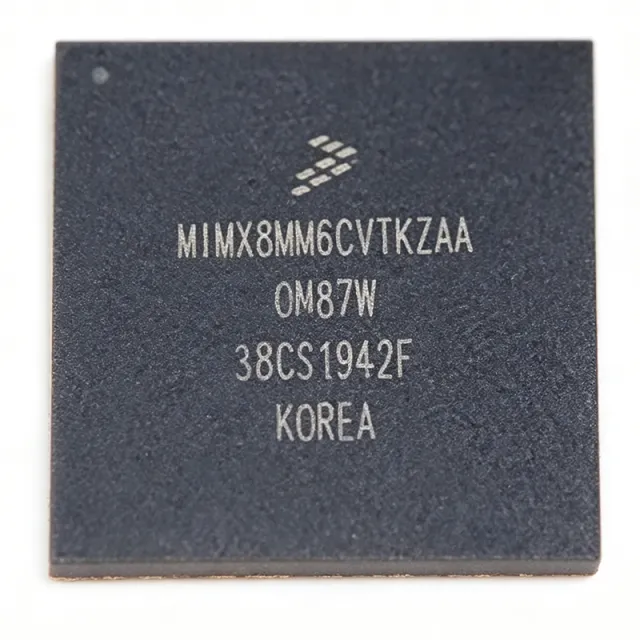
MIMX8MM6CVTKZAA - i.MX8MM Quad A53 1.6GHz SoC | NXP
MIMX8MM6CVTKZAA

MIMX8MM6CVTKZAA - i.MX8MM Quad A53 1.6GHz SoC | NXP

The NXP Semiconductors MIMX8MM6CVTKZAA is a high-performance embedded applications processor from the i.MX 8M Mini family, built on advanced 14LPC FinFET process technology. It integrates a quad-core ARM Cortex-A53 application processor running at up to 1.6GHz along with a Cortex-M4F core for real-time processing, housed in a 486-ball LFBGA package (14x14 mm) for industrial and consumer applications balancing performance, power efficiency, and multimedia capabilities. An applications processor is a system-on-chip (SoC) designed to run operating systems such as embedded Linux and complex application software on ARM architecture. It integrates CPU cores, memory controllers, graphics, and I/O interfaces, serving as the main processing unit in smart home hubs, IoT gateways, and industrial control systems. The i.MX 8M Mini sits between the lower-power i.MX 6 series and the higher-performance i.MX 8M Quad/Plus in the embedded processor hierarchy. Key features include the 64-bit quad-core Cortex-A53 cluster at 1.6GHz, a Cortex-M4F core for low-latency deterministic control, a 3D GPU (GC NanoUltra), a 2D GPU, and a 4K VPU for video encode/decode. Memory support covers LPDDR4/DDR4, and connectivity includes Gigabit Ethernet, USB 3.0, PCIe, and multiple display interfaces. Technically, the 14LPC FinFET process delivers improved power efficiency versus older planar nodes. The heterogeneous multicore architecture partitions tasks between the A53 cluster and the M4F core, enabling efficient power management. TrustZone support provides secure boot and secure execution for secure IoT deployments. Typical applications include smart home hubs, IoT gateways, industrial HMI, medical devices, and multimedia streaming devices, where combined CPU, GPU, VPU, and connectivity resources suit edge computing and AI inference. Design tip: pay careful attention to power sequencing and thermal management. The 486-ball LFBGA requires a multi-layer PCB with thermal vias and a solid ground plane, plus proper decoupling capacitors near power pins for stable operation.

USD $16.40 お問い合わせ
MIMX8QM5CVUFFAB - i.MX 8QuadMax 8-Core SoC | NXP | 1313-BGA
MIMX8QM5CVUFFAB

MIMX8QM5CVUFFAB - i.MX 8QuadMax 8-Core SoC | NXP | 1313-BGA

The NXP Semiconductors MIMX8QM5CVUFFAB is the i.MX 8QuadMax application processor, a heterogeneous eight-core System on Chip (SoC) integrating two Arm Cortex-A72, four Arm Cortex-A53, and two Arm Cortex-M4F cores in a 1313-ball FBGA package measuring 29x29 mm with automotive temperature grade. An SoC (System on Chip) consolidates CPU, GPU, memory interfaces, and peripheral controllers into a single integrated circuit, forming the complete computing heart of an embedded system. The i.MX 8QuadMax sits at the top of the NXP i.MX 8 family (alongside 8QuadPlus and 8DualMax), targeting high-performance automotive, industrial, and consumer platforms that need advanced graphics, vision processing, and deterministic real-time control in one device. Key features include full-chip hardware virtualization with domain protection for secure multi-OS operation, independent graphics across four HD displays or one 4K screen, an integrated vision pipeline for ADAS-class perception, and an audio subsystem optimized for voice and speech recognition. The dual Cortex-A72 cores handle heavy application workloads, the quad Cortex-A53 cores provide power-efficient scaling, and the dual Cortex-M4F cores run real-time, safety-relevant tasks - a heterogeneous balance of throughput and efficiency. The architecture supports Android, Linux, FreeRTOS, QNX, Green Hills, and Dornerworks XEN operating systems, and the family offers pin- and power-compatible packages for hardware design reuse. Typical applications include automotive digital cockpits, infotainment, ADAS vision systems, industrial HMI panels, and medical imaging equipment, where rich UI and real-time control must coexist. Design consideration: the 1313-ball BGA demands a multi-layer PCB with thermal vias and strict power sequencing; the MSL 3 rating (168-hour floor life) requires controlled moisture handling before reflow.

見積もり お問い合わせ
MIMXRT1061CVJ5B - 528MHz Cortex-M7 MCU | NXP | Industrial
MIMXRT1061CVJ5B

MIMXRT1061CVJ5B - 528MHz Cortex-M7 MCU | NXP | Industrial

The NXP Semiconductors MIMXRT1061CVJ5B is a 32-bit Arm Cortex-M7 crossover microprocessor operating up to 528 MHz, packaged in a 196-ball LFBGA measuring 12 x 12 mm. The device combines real-time MCU responsiveness with high-performance crossover-processor integration, supporting demanding industrial, networking, and embedded-control applications. A crossover processor is a semiconductor category that combines microcontroller real-time operation with higher-level processing capabilities. Unlike a conventional microcontroller optimized around deterministic peripheral control, the i.MX RT1060 family provides extensive connectivity, memory interfaces, security features, and graphical-media acceleration for connected embedded systems. The Arm Cortex-M7 architecture belongs to the microcontroller processor hierarchy and executes from tightly coupled memory for predictable control performance. According to the verified product listings, the MIMXRT1061CVJ5B is identified as an RT1060 device with a 528 MHz Cortex-M7 core and a 196-LFBGA package. Distributor and aggregator listings also identify this orderable configuration as a fixed USB variant. The package uses bottom-side ball terminals and surface-mount assembly, making careful PCB escape routing and thermal management essential. The i.MX RT1060 crossover-processor family is designed to bridge MCU-class control and higher-end embedded workloads. Its integrated feature set supports connected industrial equipment, human-machine interfaces, communications infrastructure, and real-time control systems. A separate NXP cross-reference result for the DVL6B variant advertises a 600 MHz Cortex-M7 core, but that variant is not treated as a drop-in substitute because its verified frequency differs by approximately 13.6 percent and other ordering details are not established here. Typical design use includes industrial gateways, connected controllers, operator panels, building automation equipment, and networked sensors. The device can manage communication tasks alongside deterministic peripheral control without adopting a higher-power application-processor architecture. Developers should confirm memory configuration, pin multiplexing, peripheral availability, clock limits, security features, and package-level routing against the official NXP datasheet before release. For PCB implementation, follow the manufacturer land pattern, ball-pitch, via, and decoupling guidance rather than generic BGA rules. Validate high-speed memory and communication interfaces with controlled-impedance routing, continuous reference planes, and signal-integrity simulations. Production designs should also review errata, boot configuration, power sequencing, firmware support, and long-term availability. This page consolidates verified NXP and distributor information, exact package identification, application guidance, design cautions, and candid replacement analysis. It distinguishes confirmed data from parameters that still require datasheet verification so procurement and engineering teams can evaluate the part efficiently without mistaking assumptions for released specifications.

見積もり お問い合わせ
MIMXRT1061CVL5B - 600MHz Cortex-M7 Crossover MCU | NXP
MIMXRT1061CVL5B

MIMXRT1061CVL5B - 600MHz Cortex-M7 Crossover MCU | NXP

The NXP MIMXRT1061CVL5B is a 32-bit crossover microcontroller built around an ARM Cortex-M7 core running up to 528 MHz (with the silicon capable of 600 MHz in the RT1061 family) and housed in a 196-ball MAPBGA package measuring 10x10 mm. According to the NXP product page, this RT1060-family industrial-grade MCU integrates 1 MB of on-chip SRAM and supports external memory through SEMC, FlexSPI, and parallel interfaces, delivering real-time signal processing for industrial control, motor drives, and human-machine interface applications. A crossover microcontroller combines the high-performance characteristics of an application processor (e.g., GHz clock, large memory) with the deterministic real-time response and low power of a microcontroller. Within the broader taxonomy, the MIMXRT1061 sits in the crossover MCU segment bridging high-end microcontrollers and entry-level application processors, complementing NXP's i.MX 8M family. Its 196-ball MAPBGA provides ample I/O for advanced peripherals including dual Ethernet, USB, CAN-FD, and a 12-bit ADC. Key features include an integrated LCDIF controller supporting up to WXGA displays, dual FlexSPI interfaces for high-speed external flash, a 12-bit ADC with up to 20 channels, and an integrated power management IC (PMIC) companion interface. The Cortex-M7 core delivers 2.14 CoreMark/MHz performance with double-precision FPU, DSP extensions, and L1 cache (16 KB I-cache and 16 KB D-cache). Hardware encryption is provided through the Bus Encryption Engine (BEE) for secure external flash execution. The RT1061 architecture implements a 4-channel eDMA, FlexTimer (FTM) modules for PWM generation, and a flexible peripheral crossbar for pin mapping. Operating voltage spans 3V to 3.6V with internal DCDC and LDO regulators generating core rails. The device supports industrial temperature ranges of -40C to +105C for harsh-environment deployments. Typical applications include industrial HMI panels with LCD displays, motor control and field-oriented control (FOC) drives, building automation controllers, point-of-sale terminals, and edge IoT gateways. The 528 MHz operation with DSP extensions makes it suitable for predictive maintenance algorithms running on-device. When designing with this part, ensure proper PCB layout for the 196-ball MAPBGA with via-in-pad or dog-bone fanout, and follow NXP's hardware design guide for DDR3L memory routing. The internal PMIC companion requires careful sequencing of DCDC outputs for clean power-up. This page synthesizes distributor pricing, drop-in package alternatives within the RT106x family, and design notes extracted from the NXP datasheet and community support threads.

見積もり お問い合わせ
MIMXRT1062DVL6B - i.MX RT1062 600MHz Cortex-M7 MCU | NXP
MIMXRT1062DVL6B

MIMXRT1062DVL6B - i.MX RT1062 600MHz Cortex-M7 MCU | NXP

The NXP MIMXRT1062DVL6B is a high-performance crossover microprocessor featuring an Arm Cortex-M7 core running at 600 MHz with 1 MB of on-chip SRAM, housed in a 196-ball LFBGA (10x10 mm) package. It belongs to the i.MX RT1060 family, blending microcontroller responsiveness with application-processor throughput for consumer products. The device integrates advanced peripherals including an LCD controller, 2D graphics accelerator (PxP), CSI camera interface, and FlexSPI for external memory expansion. What is a crossover processor? A crossover processor combines the real-time deterministic behavior of a microcontroller (MCU) with the high performance and rich multimedia features of an application processor (MPU). It bridges the architectural gap between Cortex-M MCUs and Cortex-A MPUs, sitting in the product-type hierarchy as: microcontroller -> crossover processor -> embedded processor -> semiconductor IC. This category targets applications requiring real-time DSP, graphics, and high-speed connectivity without the overhead of a full Linux-capable MPU. Key features include 600 MHz Cortex-M7 with single-precision and double-precision FPU, 1 MB on-chip SRAM, dual FlexSPI for QSPI/NOR/NAND expansion, integrated LCDIF display controller up to WXGA resolution, USB 2.0 OTG with PHY, 10/100 Mbit Ethernet MAC, 8-bit CMOS sensor interface (CSI), and 2D PxP engine. The part operates from 0.95 V to 1.05 V core and 3.0 V to 3.6 V I/O supplies, with industrial-grade temperature support. The architecture leverages the Cortex-M7 superscalar pipeline with tightly-coupled memory for deterministic interrupt response, paired with NXP's SmartDMA and eFuse-based secure boot. The 196-ball LFBGA provides ample I/O routing for high-speed parallel buses and multiple serial interfaces (SPI, I2C, UART, CAN, FlexCAN, SAI). Hardware cryptography via CAAM and TrustZone-M for isolation are integrated for secure IoT edge designs. Typical applications include HMI panels for industrial and home appliances, USB audio devices with display, motor control inverters, smart-home gateways, low-cost HMI for IoT edge nodes, and point-of-sale terminals. The wide peripheral set lets designers replace legacy MCU + external controller stacks with a single chip. When designing with this part, ensure the PCB provides sufficient thermal dissipation; the LFBGA package requires 6-layer stack-up with microvia-in-pad for reliable BGA assembly. SDRAM traces must be length-matched within 50 mils for DDR operation. Use the NXP MCUXpresso SDK and Config Tools for peripheral initialization and pin muxing. This page synthesizes distributor pricing, pin-compatible i.MX RT1060 family drop-in alternatives, and practical design considerations not aggregated on a single manufacturer or distributor page.

見積もり お問い合わせ
MIMXRT1064CVJ5B - 528MHz Cortex-M7 Crossover MCU | NXP
MIMXRT1064CVJ5B

MIMXRT1064CVJ5B - 528MHz Cortex-M7 Crossover MCU | NXP

The NXP MIMXRT1064CVJ5B is a high-performance crossover microcontroller featuring an Arm Cortex-M7 core running at 528 MHz, 4 MB on-chip flash, and 1 MB SRAM, housed in a 196-ball LFBGA (12x12 mm) package. As a member of the i.MX RT1060 family, the part bridges the gap between Application Processors and traditional microcontrollers by delivering application-processor-class compute in an MCU-style footprint. A crossover MCU (also called a crossover processor or hybrid MCU) is a class of microcontrollers that combines the high CPU performance and rich peripherals of an applications processor with the deterministic real-time response and ease-of-use of a microcontroller. The MIMXRT1064CVJ5B inherits this architecture, sitting in the broader taxonomy of microcontroller -> embedded MCU -> crossover MCU -> real-time control processor -> semiconductor. It is engineered for industrial IoT, HMI, and motor-control applications that demand both high throughput and deterministic real-time behavior. Key features include 4 MB on-chip flash, 1 MB SRAM (configurable as TCM, OCRAM, or DTCM), dual USB 2.0 OTG controllers with PHY, integrated 2D graphics acceleration engine (PxP), MIPI-CSI and parallel display interfaces, hardware encryption (AES, TRNG, secure boot), and 3x FlexCAN plus 2x Ethernet (10/100M). The 196-LFBGA package exposes a rich GPIO set and a wide peripheral mix designed to replace multi-chip MCU+DRAM solutions with a single BGA. The internal bus matrix and dual-issue pipeline allow the Cortex-M7 core to execute from tightly-coupled memory with single-wait-state access, enabling benchmark scores above 1280 CoreMark while keeping interrupt latency deterministic. On-chip regulators, integrated power management, and support for low-power modes make the device suitable for both line-powered industrial designs and battery-aware edge nodes. Typical applications include industrial human-machine interfaces, edge IoT gateways, motor control drives, audio subsystems, and graphics-rich consumer devices. The wide peripheral set also suits Point-of-Sale terminals, building automation, and connected appliances. Designers choose this part when they need Cortex-M7-class DSP and FPU throughput without migrating to a Linux-capable MPU. When designing with this device, allocate sufficient PCB copper under the BGA for thermal dissipation and route high-speed interfaces (MIPI-CSI, parallel display, RMII) with controlled-impedance traces. Plan supply sequencing for the multiple internal rails and follow the NXP hardware development guide for boot mode configuration (boot source, SD/eMMC, SPI flash) to avoid bricked prototypes. This page consolidates distributor pricing for the 196-LFBGA package, drop-in i.MX RT1064 family variants, and practical design considerations not always obvious from the manufacturer datasheet, helping procurement, EE, and firmware engineers choose the right crossover MCU for industrial and IoT designs.

見積もり お問い合わせ
MIMXRT1064CVL5A - 528MHz Cortex-M7 MCU 4MB Flash | NXP i.MX RT1064
MIMXRT1064CVL5A

MIMXRT1064CVL5A - 528MHz Cortex-M7 MCU 4MB Flash | NXP i.MX RT1064

The NXP Semiconductors MIMXRT1064CVL5A is a 32-bit crossover microcontroller built around the Arm Cortex-M7 core running at up to 528 MHz, with 4 MB of on-chip flash and 1 MB of on-chip SRAM, housed in a 196-pin LFBGA package. It provides real-time deterministic performance with rich multimedia peripherals, dual USB, 10/100 Mbit Ethernet, and an LCD controller suitable for industrial HMI. Background: A crossover microcontroller (cMCU) combines the deterministic real-time response of a microcontroller (MCU) with the high CPU performance and multimedia features typical of a microprocessor (MPU). The i.MX RT1064 belongs to the i.MX RT family, which occupies the architectural niche between traditional Cortex-M microcontrollers (no MMU, no on-chip flash) and Cortex-A microprocessors (full application processor). The 'RT' suffix signals real-time control with no external SDRAM requirement at boot because of the integrated 4 MB flash - this is the first i.MX RT family member to include on-chip flash according to NXP documentation. Key features include the 528 MHz Cortex-M7 core with single-precision and double-precision FPU, 4 MB on-chip flash, 1 MB on-chip SRAM (configurable as TCM and OCRAM), dual USB 2.0 with PHY, 10/100 Mbit Ethernet MAC, 8/16-bit CSI camera interface, 24-bit LCD controller up to WXGA resolution, and a wide range of serial interfaces (UART, SPI, I2C, I2S, FlexIO, FlexCAN, FlexPWM). The LFBGA-196 package provides ample I/O for industrial gateway, motor drive, and HMI applications. Typical applications include industrial HMI panels, IoT gateways, motor control and drives, audio subsystems, point-of-sale terminals, and smart appliance controllers. The integrated LCD controller and 2D graphics acceleration GPU enable cost-effective graphical touch interfaces without an external graphics controller. Design consideration: the LFBGA-196 package requires a 4-layer minimum PCB with microvia or laser-drilled via technology for fan-out. Plan for thermal copper mass under the exposed die paddle and verify IO bank voltage sequencing against the System Reset and Boot Mode Reference Manual before finalizing the schematic. This page synthesizes distributor pricing, drop-in alternatives, and practical design notes not found in the manufacturer datasheet.

見積もり お問い合わせ