製品 (39,000+)

MSP430F5438AIZQWR - 25MHz 256KB MCU | Texas Instruments
MSP430F5438AIZQWR

MSP430F5438AIZQWR - 25MHz 256KB MCU | Texas Instruments

The Texas Instruments MSP430F5438AIZQWR is a 25 MHz, 16-bit mixed-signal microcontroller with 256 KB of flash memory, 16 KB of SRAM, and a 12-bit ADC in a 113-ball Microstar Junior BGA package. It integrates DMA, UART, SPI, I2C, timers, and a hardware multiplier for compact embedded control and sensor-processing designs. A mixed-signal microcontroller combines a digital processor core with peripherals designed to acquire and process analog signals. The MSP430F5438AIZQWR belongs to the MSP430 family of ultra-low-power 16-bit RISC microcontrollers, where CPU processing, communication, timing, and data acquisition are integrated into one device. This makes it suitable for embedded systems that require local sensing, control, and serial communications while keeping component count low. The device provides 256 KB of flash, 16 KB of SRAM, a 25 MHz clock, and a high-performance 12-bit ADC. Its communication peripherals include UART, SPI, and I2C, while DMA supports efficient transfers without repeatedly involving the CPU. The integrated hardware multiplier accelerates suitable arithmetic operations, and three 16-bit timers support periodic events, timing, and control-loop functions. These peripherals make the MCU appropriate for industrial instrumentation, data acquisition, building automation, and low-power embedded control. The MSP430 architecture supports low-power-oriented embedded designs, particularly when the firmware can use its timers, interrupts, and serial interfaces to avoid continuous processor activity. Peripheral integration reduces the need for separate interface or conversion ICs, while DMA can improve responsiveness when moving ADC, communication, or memory data. The 113-ball package provides substantial I/O connectivity, but its fine-pitch BGA construction requires careful PCB layout, inspection, and assembly capability. Typical applications include sensor nodes, industrial measurement systems, building-control equipment, portable instruments, communication modules, and embedded data loggers. UART, SPI, and I2C allow connection to sensors, transceivers, displays, storage devices, and external controllers. The 12-bit ADC supports analog measurement, while DMA and timers help implement responsive acquisition and control tasks. When designing around this MCU, validate the complete 113-ball pinout and power requirements against the manufacturer datasheet before layout. Confirm that the PCB assembly process supports the package, provide suitable decoupling and analog routing around the ADC, and verify all unused BGA balls according to the device guidelines. Pricing and availability should be checked for the exact orderable MPN. This page combines verified manufacturer and distributor information with package, application, comparison, and design guidance intended to make component selection more practical. It is not a substitute for the complete datasheet, which remains the authoritative source for electrical limits, timing, pin definitions, and errata.

見積もり お問い合わせ
MSP430F5438AIZQWT - 25MHz 256KB Mixed-Signal MCU | TI
MSP430F5438AIZQWT

MSP430F5438AIZQWT - 25MHz 256KB Mixed-Signal MCU | TI

The Texas Instruments MSP430F5438AIZQWT is a 25 MHz, 16-bit mixed-signal microcontroller with 256 KB flash memory, 16 KB SRAM, and a 113-ball Microstar Junior BGA package. According to the verified product data, it combines an MSP430 RISC core, 31 I/O ports, a 12-bit ADC, DMA, UART, SPI, I2C, timers, and a hardware multiplier in an industrial-temperature ultra-low-power design. A mixed-signal microcontroller is a semiconductor that combines a digital processor, memory, and analog or communication peripherals on one device. The MSP430 belongs to the low-power MCU hierarchy and is designed for embedded control, measurement, communications, and battery-operated systems where efficient code execution and multiple low-power operating modes are important. This part is positioned between a general-purpose microcontroller and a dedicated signal-processing controller. Verified features include a 2.4 V to 3.6 V supply range, 25 MHz clock speed, 256 KB flash, 16 KB SRAM, 31 I/O ports, and a 12-bit ADC. The datasheet search data also identifies ultra-low-power modes including LPM3 with watchdog timer and LPM4 with RAM retention/off-related operation. The available product information further confirms UART, SPI, I2C, DMA, timers, and hardware-multiplier support, making the MCU suitable for connected industrial, sensor, and embedded-control designs. The device uses a mixed-signal architecture rather than a dedicated analog signal-processing front end. Its ADC supports embedded measurements, while serial interfaces allow connection to sensors, transceivers, memories, and human-interface modules. The 256 KB flash capacity provides substantially more program storage than smaller MSP430 devices, while the 16 KB SRAM supports working state, buffers, stacks, and peripheral data handling. Typical applications include industrial sensor nodes, low-power data loggers, building-control equipment, battery-powered monitors, communications equipment, and compact embedded systems. The 113-ball Microstar Junior package supports dense PCB layouts, but its ball pitch, exposed thermal requirements, assembly process, and layout rules must be checked against the official package drawing before layout. For a robust design, confirm the exact package pinout, power sequencing, decoupling requirements, clock configuration, ADC reference, and low-power wake-up behavior in the manufacturer datasheet. This page distinguishes verified values from parameters requiring project-specific confirmation and avoids treating distributor snippets as complete electrical specifications.

見積もり お問い合わせ
MSP430F5438IPZ - 25MHz, 256KB MCU with 12-bit ADC | TI
MSP430F5438IPZ

MSP430F5438IPZ - 25MHz, 256KB MCU with 12-bit ADC | TI

The Texas Instruments MSP430F5438IPZ is a 16-bit ultra-low-power mixed-signal microcontroller with a 25 MHz MSP430 CPU, 256 KB flash memory, 16 KB SRAM, and a 12-bit ADC in a 100-LQFP package. It combines a RISC processor, hardware multiplier, DMA, four UART/USCI peripherals, SPI, and I2C support for embedded control, measurement, and communication systems. A microcontroller is a programmable integrated circuit that combines a CPU, memory, peripherals, and I/O in one device. The MSP430 family uses a 16-bit RISC architecture with 16-bit registers and constant generators, supporting efficient control and signal-processing workloads. The MSP430F5438 belongs to the MSP430F5xx family of mixed-signal MCUs, combining digital control with analog measurement and low-power operating modes. Key features include 256 KB of flash, 16 KB of SRAM, a 12-bit ADC, a hardware multiplier, DMA, four USCI peripherals, timers, and a real-time clock. The device is suitable for industrial instrumentation, sensor acquisition, low-power embedded control, communications, and signal-processing applications. Its 14 x 14 mm 100-LQFP package provides a conventional surface-mount footprint with numerous external peripheral connections. The MSP430F5438 product page identifies a 25 MHz operating speed and 256 KB flash, while the MSP430F5438IPZ distributor listing specifies the 100-LQFP (14 x 14) package and 16-bit MCU architecture. The mixed-signal design allows firmware to acquire analog inputs and control digital peripherals without requiring separate analog or communications devices. Typical designs use the ADC for sensor and analog signal measurement, UART or SPI for external devices, I2C for sensors and memory, DMA for efficient peripheral transfers, and timers for precise event control. The MSP-EXP430F5438 experimenter-board ecosystem provides a relevant development context, while the MSP430 hardware tools user guide is identified as a reference for supported target devices. When designing a board around this MCU, verify the exact pin functions, power requirements, clock configuration, and peripheral multiplexing in the MSP430F5438 datasheet. Place decoupling close to the power pins and route sensitive analog inputs away from high-current switching nodes. The verified distributor listing identifies an 18 MHz CPU entry, while the manufacturer product page identifies a 25 MHz MCU; these values should be reconciled against the exact device revision and operating conditions before release. This page synthesizes verified manufacturer and distributor specifications, package information, application guidance, and procurement references for engineers evaluating the MSP430F5438IPZ.

見積もり お問い合わせ
MSP430F5438IPZR - 25MHz, 256KB Flash MCU | Texas Instruments
MSP430F5438IPZR

MSP430F5438IPZR - 25MHz, 256KB Flash MCU | Texas Instruments

The Texas Instruments MSP430F5438IPZR is a 16-bit mixed-signal microcontroller operating at up to 25 MHz, with 256 KB of flash memory, 16 KB of SRAM, and a 12-bit ADC, supplied in a 100-pin LQFP package. It integrates DMA, UART, SPI, I2C, timers, and a hardware multiplier for embedded control and low-power applications. A mixed-signal microcontroller combines a digital processor core with analog and communication peripherals, allowing one device to control sensors, communications, timers, and power sequencing. The MSP430 belongs to the microcontroller -> embedded processor -> semiconductor hierarchy and is designed for battery-powered and industrial systems that require efficient computation and broad peripheral integration. The verified manufacturer and distributor information identifies the MSP430F5438 family with 25-MHz operation, 256-KB flash, 16-KB SRAM, a 12-bit ADC, DMA, UART, SPI, I2C, timers, and a hardware multiplier. These resources support mixed-signal acquisition, data movement, motor and timer control, sensor conditioning, and low-power embedded products. The MSP430F5438IPZR ordering code identifies the 100-LQFP, 14 x 14 mm package and the IPZR package/reel ordering variant. The distributor listing also identifies the CPUXV2 MSP430F5xx microcontroller class. The available verified data does not include the complete electrical limits, ADC timing, memory-map details, GPIO count, or pin names, so those values must be confirmed in the manufacturer datasheet before design release. Typical uses include industrial sensor nodes, portable measurement equipment, data-acquisition systems, communications controllers, low-power industrial controls, and embedded motor or timer systems. The integrated ADC and communication peripherals can reduce external component count, while the large flash and SRAM footprint supports firmware, protocol stacks, buffering, and application logic. Design with the MSP430F5438IPZR by confirming the exact pinout, power-supply limits, clock configuration, reset behavior, and peripheral multiplexing in the TI datasheet. Keep analog inputs, supply returns, and high-speed communications appropriately routed on the PCB, and validate low-power modes against the application’s wake-up and measurement requirements. This page consolidates verified manufacturer and distributor information, package data, commercial search results, and engineering-oriented application guidance. It intentionally identifies missing electrical details rather than estimating them, helping engineers distinguish documented facts from values that require final datasheet verification.

見積もり お問い合わせ
MSP430F5507IRGZR - 25MHz MCU, 32KB Flash, USB 2.0 | Texas Instruments
MSP430F5507IRGZR

MSP430F5507IRGZR - 25MHz MCU, 32KB Flash, USB 2.0 | Texas Instruments

The Texas Instruments MSP430F5507IRGZR is a 16-bit ultra-low-power mixed-signal microcontroller from the MSP430F5xx family, integrating a 25 MHz MSP430 CPUXV2 core with 32KB Flash, 6KB SRAM (one source quotes 4KB), a 10-bit ADC, DMA, UART/SPI/I2C serial interfaces, hardware multiplier, multiple timers, and a USB 2.0 full-speed peripheral. The device is housed in a 48-pin VQFN (RGZ) package measuring 7x7 mm with an exposed thermal pad. An MSP430 microcontroller is a 16-bit RISC mixed-signal MCU platform from Texas Instruments that occupies the low-power and battery-aware tier of the embedded MCU hierarchy. Within that platform hierarchy the device sits as: MSP430F5xx -> MSP430F55xx (USB sub-family) -> MSP430F550x -> MSP430F5507. The 'F' prefix indicates in-system programmable Flash, the '5' indicates the F5xx generation with the CPUXV2 core and 25 MHz operation, and the trailing digits indicate memory size and feature set. The platform is widely used where deterministic low power and integrated analog matter more than raw MHz. Key differentiating features include active-mode current of 180-195 uA/MHz at 3V, standby current of a few uA, a 1.4 V to 3.6 V wide core supply range (3.6 V absolute max), a true hardware USB 2.0 full-speed transceiver on-chip, a 10-bit successive-approximation ADC with up to 12 external input channels and sample-and-hold, a 32-bit hardware multiplier that accelerates DSP routines, and 31 general-purpose I/O pins. The internal oscillator removes an external crystal in many designs, and the DMA controller offloads data movement between peripherals and memory. At the architectural level, the device uses TI's von-Neumann unified memory map with a 16-bit CPUXV2 core, a 3-stage pipeline, and four hardware multiplier operating modes. The integrated USB peripheral includes an on-chip PHY and pull-up resistors; code can implement HID, CDC, or vendor-class stacks directly. The 10-bit ADC is shared across eight internal and up to twelve external channels through the analog mux, while the DMA engine can stream ADC conversions directly into memory without CPU intervention. Typical applications include USB human-interface devices such as keyboards, mice, and game controllers; portable medical and wellness peripherals; industrial sensor nodes and data loggers; low-power metering; and battery-powered instrumentation that needs an MCU + USB in a single chip. The wide I/O count and integrated analog make it a good fit when an external ADC or signal-conditioning chain would otherwise inflate the BOM. When designing with this part, follow the TI MSP430x5xx Family User's Guide for power-management sequencing, especially the wake-from-LPM transitions and the USB suspend current budget. Reserve the exposed thermal pad for soldering to a ground copper pour to meet the package's thermal-resistance spec and to reduce EMI on the USB DP/DM lines. Use TI's USB Descriptor Tool and MSP430 USB Developers Package firmware to accelerate stack bring-up. This page synthesizes distributor pricing from DigiKey/Mouser/LCSC, verified same-family drop-in alternatives, and practical design notes for USB-aware embedded systems that are not always consolidated in the manufacturer datasheet.

見積もり お問い合わせ
MSP430F5510CY - 25MHz 16-Bit MCU with 32KB Flash | TI
MSP430F5510CY

MSP430F5510CY - 25MHz 16-Bit MCU with 32KB Flash | TI

The Texas Instruments MSP430F5510CY is a 25 MHz, 16-bit mixed-signal microcontroller with 32KB of Flash memory, 4KB of SRAM, a 10-bit ADC, comparator, DMA, UART, SPI, I2C, USB, and a hardware multiplier. The MSP430F5510CY ordering code identifies a die-sale form of the MSP430F5510 family rather than a leaded or surface-mount package. A mixed-signal microcontroller is an integrated circuit that combines a programmable digital controller with analog measurement or comparison functions. In the product hierarchy, the MSP430F5510 belongs to the MSP430 mixed-signal microcontroller family, which is a type of 16-bit embedded processor and system-on-chip. Its combination of low-power-oriented control, serial interfaces, USB connectivity, and analog peripherals allows sensing and control tasks to be consolidated in compact embedded systems. The principal verified specifications are a 25 MHz maximum clock, 32KB Flash organized as 32K x 8, 4KB SRAM, and a 10-bit ADC. The device also provides a comparator, DMA controller, UART, SPI, I2C, USB interface, and hardware multiplier. These resources support applications that require periodic analog sampling, event-driven data transfer, low-rate communication, or multiplication-intensive control without requiring a separate analog front end for every function. The MSP430F5510 uses the MSP430 CPUXV2 architecture and belongs to the MSP430F5xx mixed-signal family. DMA can move data independently of the CPU, while the hardware multiplier accelerates multiplication tasks. The parallel availability of UART, SPI, and I2C permits a designer to connect sensors, displays, storage devices, and other embedded modules while retaining USB for a host-oriented interface. Exact ADC timing, USB details, clock configuration, and electrical limits should be confirmed in the manufacturer datasheet before final design release. Typical uses include industrial sensor nodes, compact USB-connected data collectors, building and equipment controls, low-power monitoring equipment, and mixed-signal instruments. In an analog-monitoring design, the 10-bit ADC can acquire sensor signals while the comparator handles threshold events and DMA transfers results into SRAM. UART, SPI, or I2C can then connect the controller to local peripherals, while USB provides a higher-level connection when required. The most important design consideration for the MSP430F5510CY is that CY is a die-sale device rather than a finished, pin-defined package. Its footprint, assembly process, bonding method, die orientation, and exposed features therefore require direct coordination with the assembly provider. Engineers must also verify clock, memory, USB, analog, and power requirements against the MSP430F5510 datasheet and validate the assembled board before production. This page consolidates the verified manufacturer specifications, current distributor pricing reference, die-sale packaging information, application guidance, and the documented absence of a confirmed drop-in replacement. It also distinguishes verified facts from package-specific information that cannot be inferred from the bare-die ordering code.

見積もり お問い合わせ
MSP430F5519IPN - 25MHz 128KB Flash USB MCU | Texas Instruments (Tape & Reel)
MSP430F5519IPN

MSP430F5519IPN - 25MHz 128KB Flash USB MCU | Texas Instruments (Tape & Reel)

The Texas Instruments MSP430F5519IPN is a 25 MHz, 16-bit mixed-signal microcontroller with 128KB of flash memory, 8KB of SRAM, USB, and extensive serial connectivity in an 80-pin LQFP package. It operates from a low 1.8 V to 3.6 V supply range and supports temperatures from -40°C to +85°C, making it suitable for compact embedded systems that need low power consumption and multiple communication interfaces. The MSP430 is an ultra-low-power RISC microcontroller family designed around a 16-bit CPU, efficient register architecture, and multiple low-power operating modes. These characteristics make the MSP430F5519 appropriate for battery-powered measurement, communications, industrial control, and portable equipment where energy efficiency is a primary design constraint. Key features include a 25 MHz CPU, 128KB flash, 8KB SRAM, 63 I/O pins, a comparator, DMA, UART, SPI, I²C, USB, timers, and a hardware multiplier. The integrated connectivity and mixed-signal resources reduce the need for external peripheral devices while providing flexible interface options for sensors, actuators, and communication modules. The device uses the MSP430 CPUXV2 core, a 16-bit RISC architecture with 16-bit registers and constant generators intended to improve code efficiency. Its operating range of 1.8 V to 3.6 V supports low-voltage embedded designs, while the 80-LQFP package provides a conventional surface-mount footprint with a large number of accessible I/O pins. Typical applications include USB-connected control systems, low-power data acquisition, industrial instrumentation, sensor networks, portable measurement equipment, and embedded communications products. The combination of USB, UART, SPI, I²C, DMA, timers, comparator, and hardware multiplier allows designers to connect sensors, storage, displays, and host systems without building a complex peripheral network. When designing around the MSP430F5519IPN, verify the complete pinout, supply requirements, clock configuration, and peripheral multiplexing against the manufacturer datasheet. Decoupling, USB routing, and low-power mode entry require careful PCB and firmware planning, especially when the system combines USB connectivity with battery-operated operation.

見積もり お問い合わせ
MSP430F5519IPNR - 25MHz 128KB Flash USB MCU | Texas Instruments
MSP430F5519IPNR

MSP430F5519IPNR - 25MHz 128KB Flash USB MCU | Texas Instruments

The Texas Instruments MSP430F5519IPNR is a 25 MHz, 16-bit mixed-signal microcontroller with 128KB of flash memory, 8KB of SRAM, USB, and extensive serial connectivity in an 80-pin LQFP package. It operates from a low 1.8 V to 3.6 V supply range and supports temperatures from -40°C to +85°C, making it suitable for compact embedded systems that need low power consumption and multiple communication interfaces. The MSP430 is an ultra-low-power RISC microcontroller family designed around a 16-bit CPU, efficient register architecture, and multiple low-power operating modes. These characteristics make the MSP430F5519 appropriate for battery-powered measurement, communications, industrial control, and portable equipment where energy efficiency is a primary design constraint. Key features include a 25 MHz CPU, 128KB flash, 8KB SRAM, 63 I/O pins, a comparator, DMA, UART, SPI, I²C, USB, timers, and a hardware multiplier. The integrated connectivity and mixed-signal resources reduce the need for external peripheral devices while providing flexible interface options for sensors, actuators, and communication modules. The device uses the MSP430 CPUXV2 core, a 16-bit RISC architecture with 16-bit registers and constant generators intended to improve code efficiency. Its operating range of 1.8 V to 3.6 V supports low-voltage embedded designs, while the 80-LQFP package provides a conventional surface-mount footprint with a large number of accessible I/O pins. Typical applications include USB-connected control systems, low-power data acquisition, industrial instrumentation, sensor networks, portable measurement equipment, and embedded communications products. The combination of USB, UART, SPI, I²C, DMA, timers, comparator, and hardware multiplier allows designers to connect sensors, storage, displays, and host systems without building a complex peripheral network. When designing around the MSP430F5519IPNR, verify the complete pinout, supply requirements, clock configuration, and peripheral multiplexing against the manufacturer datasheet. Decoupling, USB routing, and low-power mode entry require careful PCB and firmware planning, especially when the system combines USB connectivity with battery-operated operation.

見積もり お問い合わせ
MSP430F5529IPN - 25MHz 128KB Flash USB MCU | Texas Instruments (Tape & Reel)
MSP430F5529IPN

MSP430F5529IPN - 25MHz 128KB Flash USB MCU | Texas Instruments (Tape & Reel)

The Texas Instruments MSP430F5529IPN is a 16-bit ultra-low-power microcontroller featuring the MSP430 CPUXV2 core running at up to 25 MHz. It integrates 128KB of Flash memory, 8KB of SRAM, a 12-bit ADC, comparator, DMA, UART/SPI/I2C, USB 2.0, and a hardware multiplier, all in an 80-pin LQFP (PN) package measuring 12x12 mm. This device is part of the MSP430F55xx family, designed for extended battery life in portable and industrial applications. A microcontroller (MCU) is a compact integrated circuit containing a processor core, memory, and programmable input/output peripherals on a single chip. The MSP430 family is renowned for its ultra-low-power operation, featuring multiple low-power modes that reduce current consumption to microamps, making it ideal for battery-powered devices. The MSP430F5529IPN sits within the MSP430F5xx series, which adds USB connectivity and enhanced analog peripherals while maintaining the low-power heritage of the MSP430 architecture. Key features include 25 MHz CPU speed, 128KB Flash, 8KB SRAM, a 12-bit ADC with up to 16 external channels, a comparator, DMA controller, two USCI modules supporting UART/SPI/I2C, a full-speed USB 2.0 interface with integrated PHY, and a 32-bit hardware multiplier. The device operates from 1.8V to 3.6V and supports a wide temperature range of -40C to +85C. The LQFP-80 package provides 63 I/O pins, enabling complex system integration. The MSP430F5529IPN employs the MSP430 CPUXV2 architecture with a von-Neumann memory layout, offering efficient code density and low power consumption. The integrated USB module supports device, host, and OTG modes, simplifying connectivity in embedded systems. The hardware multiplier accelerates DSP-like operations, while the DMA controller offloads data transfers from the CPU, improving overall system throughput. Typical applications include portable medical devices, smart meters, industrial sensor nodes, USB-based data acquisition systems, and battery-powered IoT endpoints. The combination of low power, USB, and rich analog peripherals makes it a versatile choice for designs requiring extended battery life and connectivity. When designing with this MCU, pay attention to the power supply decoupling and the USB PHY layout to ensure signal integrity. The device supports multiple low-power modes, so configure the clock system and peripherals appropriately to maximize battery life.

見積もり お問い合わせ
MSP430F5529IPNR - 25MHz 128KB Flash USB MCU | Texas Instruments
MSP430F5529IPNR

MSP430F5529IPNR - 25MHz 128KB Flash USB MCU | Texas Instruments

The Texas Instruments MSP430F5529IPNR is a 16-bit ultra-low-power microcontroller featuring the MSP430 CPUXV2 core running at up to 25 MHz. It integrates 128KB of Flash memory, 8KB of SRAM, a 12-bit ADC, comparator, DMA, UART/SPI/I2C, USB 2.0, and a hardware multiplier, all in an 80-pin LQFP (PN) package measuring 12x12 mm. This device is part of the MSP430F55xx family, designed for extended battery life in portable and industrial applications. A microcontroller (MCU) is a compact integrated circuit containing a processor core, memory, and programmable input/output peripherals on a single chip. The MSP430 family is renowned for its ultra-low-power operation, featuring multiple low-power modes that reduce current consumption to microamps, making it ideal for battery-powered devices. The MSP430F5529IPNR sits within the MSP430F5xx series, which adds USB connectivity and enhanced analog peripherals while maintaining the low-power heritage of the MSP430 architecture. Key features include 25 MHz CPU speed, 128KB Flash, 8KB SRAM, a 12-bit ADC with up to 16 external channels, a comparator, DMA controller, two USCI modules supporting UART/SPI/I2C, a full-speed USB 2.0 interface with integrated PHY, and a 32-bit hardware multiplier. The device operates from 1.8V to 3.6V and supports a wide temperature range of -40C to +85C. The LQFP-80 package provides 63 I/O pins, enabling complex system integration. The MSP430F5529IPNR employs the MSP430 CPUXV2 architecture with a von-Neumann memory layout, offering efficient code density and low power consumption. The integrated USB module supports device, host, and OTG modes, simplifying connectivity in embedded systems. The hardware multiplier accelerates DSP-like operations, while the DMA controller offloads data transfers from the CPU, improving overall system throughput. Typical applications include portable medical devices, smart meters, industrial sensor nodes, USB-based data acquisition systems, and battery-powered IoT endpoints. The combination of low power, USB, and rich analog peripherals makes it a versatile choice for designs requiring extended battery life and connectivity. When designing with this MCU, pay attention to the power supply decoupling and the USB PHY layout to ensure signal integrity. The device supports multiple low-power modes, so configure the clock system and peripherals appropriately to maximize battery life.

見積もり お問い合わせ
MSP430F5638IPZ - 20MHz 256KB Flash MCU | Texas Instruments
MSP430F5638IPZ

MSP430F5638IPZ - 20MHz 256KB Flash MCU | Texas Instruments

The Texas Instruments MSP430F5638IPZ is a 20 MHz mixed-signal microcontroller with 256 KB of Flash memory, 16 KB of SRAM, a 12-bit ADC, a 12-bit DAC, USB, DMA, and an on-chip comparator, supplied in a 100-pin LQFP package. It combines a 16-bit RISC CPU with low-power operating modes for portable measurement, industrial control, and USB-connected data-acquisition systems. An ultra-low-power microcontroller is a semiconductor designed to complete control and measurement tasks while minimizing energy consumption. The MSP430 family combines a 16-bit RISC core, 16-bit registers, constant generators, and hardware peripherals in a single mixed-signal device. Its architecture supports portable instruments that must alternate between active processing and low-power standby operation while retaining measurements, control state, and communications. Three headline characteristics distinguish this part. The 20 MHz CPU provides higher processing throughput than slower MSP430 devices, while 256 KB of Flash provides room for application code, boot routines, and firmware updates. The analog signal chain combines a 12-bit ADC and 12-bit DAC, allowing a single device to acquire sensor inputs and generate analog outputs without requiring separate converters. The integrated feature set also includes USB, DMA, and a comparator. USB supports direct connectivity to a host or peripheral system, DMA reduces CPU involvement during data transfers, and the comparator supports threshold detection and basic analog supervision. Texas Instruments identifies the MSP430F5638 family as an ultra-low-power MCU intended for portable measurement applications where low-power modes can extend battery life. Typical implementations include USB-connected sensors, precision data loggers, industrial monitoring nodes, handheld analyzers, and low-power embedded measurement instruments. The 12-bit ADC handles analog sensor conditioning, the DAC supports excitation or output signals, and USB reduces the need for a separate protocol converter when the application uses a standard USB interface. PCB design should preserve the analog signal path and USB signal integrity. Place the ADC and DAC support components close to their associated pins, provide clean reference and supply connections, and route USB differential pairs as a short, symmetric pair on a continuous reference plane. Confirm the exact pin assignments, exposed thermal-pad requirements, and decoupling recommendations in the manufacturer datasheet before layout release. This page combines the manufacturer's device features with a practical drop-in alternative assessment, package-level comparison, and engineering design notes. It highlights where the MSP430F5638IPZ fits in mixed-signal designs and where pin-compatible MCU options can support memory upgrades, production sourcing, or footprint consolidation.

見積もり お問い合わせ
MSP430F6638CY - 20MHz 16-Bit Mixed-Signal MCU | Texas Instruments
MSP430F6638CY

MSP430F6638CY - 20MHz 16-Bit Mixed-Signal MCU | Texas Instruments

The Texas Instruments MSP430F6638CY is a 20 MHz, 16-bit mixed-signal microcontroller with 256KB of Flash memory, 16KB of SRAM, a 12-bit ADC, a 12-bit DAC, a comparator, DMA, USB connectivity, and support for a 160-segment LCD. The device is identified as a die-sale product, so the MSP430F6638CY ordering code is not associated with a standard finished package in the manufacturer product information shown here. A mixed-signal microcontroller combines a digital processor with analog conversion and other peripheral functions on one integrated circuit. The MSP430F6638 belongs to the MSP430F6xx family, whose 16-bit RISC CPUXV2 architecture uses a reduced instruction set designed for efficient embedded control. USB, serial interfaces, DMA, and high-resolution analog peripherals make this device suitable for industrial instrumentation, data acquisition, communications, and control systems where integration can reduce external component count. The MSP430F6638 operates with a 20 MHz maximum clock and provides 256KB of program Flash plus 16KB of SRAM. Its analog resources include a 12-bit ADC and 12-bit DAC, while the integrated comparator supports thresholding and signal monitoring. Additional peripherals include DMA, brown-out detection and reset, power-on reset, PWM, a watchdog timer, and a 160-segment LCD driver. These features support real-time acquisition, local control loops, human-machine interfaces, and firmware-managed peripheral movement. The device provides I2C, IrDA, LINbus, SCI, SPI, UART/USART, and USB connectivity. USB can support a direct host or device-oriented peripheral role, while the serial interfaces allow connection to sensors, transceivers, displays, and external converters. The 74 I/O positions indicated for the MSP430F6638 family provide a broad hardware interface for a platform assembled from bare die or a qualified module. Because MSP430F6638CY is offered as die sale rather than a conventional packaged ordering option, assembly into a finished electronic assembly requires die attach, wire bonding, electrical verification, and a package or substrate designed for the device. The die-sale designation also means that exposed-pad, lead, pinout, and standard package drawings cannot be assigned safely without the bonding map or assembly documentation. For new production designs, engineers should use the MSP430F6638 family documentation, confirm the available memory and peripheral configuration, and plan the analog input conditioning around the ADC resolution. USB signal routing requires controlled impedance and careful placement of protection and bypass components, while firmware should verify reset behavior and watchdog behavior during startup. This product summary consolidates the manufacturer specifications, ordering information, interface capabilities, die-sale constraints, and application guidance needed to evaluate the MSP430F6638CY before beginning an embedded mixed-signal design.

見積もり お問い合わせ
MSP430F6723IPZ - 25 MHz Metering MCU | Texas Instruments
MSP430F6723IPZ

MSP430F6723IPZ - 25 MHz Metering MCU | Texas Instruments

The Texas Instruments MSP430F6723IPZ is a 16-bit ultra-low-power mixed-signal microcontroller designed for single-phase metering, with a 25 MHz maximum CPU speed, 64 KB of Flash memory, 4 KB of RAM, and two sigma-delta ADCs. It is housed in a 100-pin LQFP (PZ) package rated for -40 °C to 85 °C. A mixed-signal microcontroller combines a digital processor with analog front-end and energy-measurement peripherals on one device. The MSP430F6xx family belongs to the broader embedded MCU category and provides programmable real-time control for energy meters, utility data concentrators, industrial monitoring systems, and portable measurement equipment. Its integration reduces component count while keeping sensing, computation, display control, and communication functions within one low-power device. Key features include 72 configurable I/O pins, two 16-bit sigma-delta ADCs, LCD drive capability, and an internal real-time clock. The device operates from a 3.6 V low-supply range and is specified at 265 µA/MHz in active mode with all system clocks operating at 8 MHz and 3.0 V. These characteristics support metering designs that must continuously acquire analog energy signals while controlling a segment or matrix LCD. The MSP430 architecture uses a 16-bit RISC core with 16-bit registers and constant generators, supporting efficient metering algorithms and compact firmware. Multiple low-power operating modes help reduce energy consumption when the meter is idle, while the real-time clock allows time-of-use measurement and load-profile timing without an external clock component. Typical applications include single-phase electricity meters, smart grid endpoint equipment, industrial energy monitors, and low-cost data loggers with LCD displays. The two sigma-delta channels are particularly relevant to current and voltage sensing, where oversampled conversion and digital filtering improve signal resolution before calculations are performed by the CPU. When laying out a meter board, reserve isolated analog routing for the sigma-delta inputs and keep LCD segment, crystal, and high-current drive connections away from the measurement front end. Confirm the complete pin-assignment table in the manufacturer datasheet before routing, especially for the exposed ground and supply pins in the 100-pin LQFP footprint. This page organizes the device specifications, verified alternatives, metering application guidance, and PCB-level design considerations to support faster component selection and board bring-up.

見積もり お問い合わせ
MSP430F6734AIPNR - 16-bit 96KB Flash Metering SoC | Texas Instruments
MSP430F6734AIPNR

MSP430F6734AIPNR - 16-bit 96KB Flash Metering SoC | Texas Instruments

The Texas Instruments MSP430F6734AIPNR is a single-phase metering system-on-chip (SoC) built around the 16-bit MSP430 CPUXV2 core running at up to 25 MHz, integrating 96 KB Flash and 4 KB RAM in an 80-pin LQFP (PN) package measuring 12 x 12 mm. It is purpose-engineered for metrology and energy-meter front-ends, combining three independent 24-bit sigma-delta analog-to-digital converters, an on-chip real-time clock, hardware LCD driver, and the ultra-low-power MSP430 architecture to deliver years of battery life on a single lithium cell. Background: A metering SoC is a class of mixed-signal microcontroller optimized for accurate measurement of line-voltage and line-current waveforms in single- or poly-phase electricity meters. Within the broader power-management IC hierarchy, the metering SoC sits alongside analog front-ends (AFEs), metrology coprocessors, and standard MCUs, but uniquely combines the metering-specific sigma-delta data path, reference, and LCD segment drive into a single low-power die. This integration eliminates the need for a dedicated metrology AFE companion chip and reduces BOM count. Key differentiating features include the three 24-bit sigma-delta ADCs with built-in programmable gain amplifiers, dedicated tamper-detection input pins for anti-tamper designs, hardware RTC with calendar function, integrated segmented LCD driver supporting up to 320 segments, and the MSP430 CPUXV2 core offering multiple low-power modes (LPM3, LPM4) with sub-microamp standby current. The 96 KB Flash supports full application firmware plus IEC 62053-22 calibration tables. Technical depth: The three sigma-delta ADCs are paired with on-chip voltage reference and gain stages, enabling simultaneous sampling of phase voltage, phase current, and neutral current with effective number of bits (ENOB) suitable for Class 0.2 or Class 0.5 meters per IEC 62053. The 25 MHz CPUXV2 core provides ample headroom for FFT-based harmonic analysis up to the 63rd harmonic while remaining in active mode only during measurement windows. Typical applications include single-phase residential electricity meters, smart energy monitoring sockets, energy-harvesting IoT sensors, prepayment meters, and battery-backed tamper-detecting metering nodes. The integrated LCD driver eliminates a separate driver chip and reduces cost in display-equipped designs. Compared with a discrete MCU + AFE solution, the SoC approach reduces PCB area by approximately 40% and BOM cost. Design consideration: When laying out the PCB, keep the analog sigma-delta traces short and symmetric to avoid degrading effective resolution, place the 32.768 kHz crystal within 5 mm of the XIN/XOUT pins, and provide a solid ground plane under the device to minimize noise coupling into the metrology inputs. This page synthesizes distributor pricing, drop-in alternative MPNs, and design guidance not consolidated in the manufacturer datasheet, supporting rapid component selection and second-sourcing decisions.

見積もり お問い合わせ
MSP430F6736AIPN - 25MHz Metering SoC MCU 128KB Flash | TI
MSP430F6736AIPN

MSP430F6736AIPN - 25MHz Metering SoC MCU 128KB Flash | TI

The Texas Instruments MSP430F6736AIPN is a 16-bit ultra-low-power microcontroller SoC designed for single-phase electricity metering, integrating three independent 24-bit Sigma-Delta ADCs, an LCD driver, real-time clock (RTC), 128KB of Flash, and 8KB of RAM in an 80-pin LQFP (PN) package. It runs the MSP430 CPUXV2 core at up to 25 MHz and operates from 2.5V or 3.3V supplies across -40C to +85C, with rich connectivity including I2C, IrDA, LINbus, SCI, SPI, and UART/USART. A metering SoC (System-on-Chip) is a microcontroller that integrates application-specific analog front-end peripherals - in this case, three precision Sigma-Delta analog-to-digital converters - directly onto the same silicon as the CPU, memory, and display drivers. This topology eliminates the need for an external ADC chip in single-phase energy-meter products, reducing BOM cost and PCB area. The MSP430F6736AIPN sits inside TI's MSP430F6xx metering family, which extends from the broader MSP430 ultra-low-power MCU lineage into the power-measurement domain. Synonyms commonly used in the trade include 'metering MCU', 'energy-meter SoC', and 'e-meter microcontroller'. Key differentiating features of the MSP430F6736AIPN include its 128KB of in-system programmable Flash (sufficient for storing calibration tables, metrology algorithms, and display fonts), an integrated segmented-LCD driver that eliminates external LCD bias-generation hardware, the three 24-bit Sigma-Delta ADCs which simultaneously sample voltage and current channels for class-0.2 or class-0.5 energy accuracy, and ultra-low-power modes that allow the entire meter to draw under 4 mA active while continuously metering. Technically, the device combines a 16-bit RISC MSP430 CPUXV2 core with hardware multiplier, an embedded RTC with calendar, brown-out reset, supply-voltage supervisor, watchdog timer, and multiple timer/capture modules. The three SD24 ADCs achieve effective resolution suitable for IEC 62053-22 class-0.2 meters, and the integrated LCD driver supports up to 320 segments in 8-mux mode. The 80-pin LQFP package exposes all analog and digital pins, with the PN suffix identifying a 12x12 mm body. Typical applications include single-phase residential electricity meters, smart-plug energy monitors, in-home display panels, sub-metering for solar inverters, and industrial power-monitoring controllers. The combination of three SD ADCs and an LCD driver makes the part a true single-chip solution for IEC-compliant class meters. When designing with this device, place the crystal and the SD24 RC components as close to the respective pins as the layout allows, route the analog and digital grounds as separate nets joined at a single point near the IC, and follow TI's 'Single-Phase Metering with the MSP430F6736A' reference design for ADC gain calibration. This page consolidates distributor pricing, drop-in package-matched alternatives, application notes, and design guidance that go beyond a single datasheet table, giving engineers a faster path from datasheet to working single-phase meter prototype.

見積もり お問い合わせ
MSP430F6736AIPNR - 128KB Flash 16-Bit Metering SoC | TI
MSP430F6736AIPNR

MSP430F6736AIPNR - 128KB Flash 16-Bit Metering SoC | TI

The Texas Instruments MSP430F6736AIPNR is a 16-bit RISC ultra-low-power single-phase metering system-on-chip (SoC) with three independent 24-bit sigma-delta ADCs, an integrated LCD driver, real-time clock, 128 KB Flash and 8 KB RAM, packaged in an 80-pin LQFP (PN) at 12x12 mm. The CPU core runs at up to 25 MHz and the device supports 1.8V-3.6V supply with active-mode current typically in the 200-400 uA/MHz range, suitable for line-powered and battery-aware smart-meter designs. A single-phase metering SoC is a microcontroller with on-chip analog front-end and LCD driver, purpose-built to perform metrology calculations (RMS voltage, RMS current, active/reactive power, energy) for one residential or commercial phase. The MSP430 family belongs to the broader hierarchy: metering MCU -> mixed-signal microcontroller -> 16-bit microcontroller -> ultra-low-power MCU -> embedded processor. Sigma-delta ADCs offer 24-bit resolution at low sample rates, ideal for current transformers and shunt-based sensing where high dynamic range and noise rejection matter more than bandwidth. Key features include three 24-bit sigma-delta ADCs with differential inputs and programmable gain, hardware AES-256 accelerator on most F67xxA derivatives, integrated LCD driver supporting up to 320 segments, on-chip RTC with calendar, brown-out reset, supply voltage supervisor, and a multi-channel 10-bit SAR ADC on shared pins. Communication interfaces include up to four USCI modules supporting UART/SPI/I2C, IrDA encoder/decoder, and JTAG/SBW for in-system programming and debugging. The MSP430F6736AIPNR uses TI's MSP430 CPUXV2 16-bit RISC core with a 16-bit register file, hardware multiplier, and four-byte fetch. Code execution from Flash at 25 MHz delivers 1.46 DMIPS/MHz (Whetstone equivalent). The architecture trades absolute throughput for energy efficiency: each peripheral can be individually clock-gated, and the CPU enters one of five low-power modes (LPM0-LPM4) with standby currents below 1 uA. Typical applications include single-phase electricity meters (Class 0.2/0.5/1.0 accuracy), smart energy monitoring plugs, solar PV string monitors, appliance line-monitoring controllers, and any battery-aware IoT sensor requiring an integrated LCD. Pin compatibility with the F6736A family allows easy migration to higher-memory or lower-cost variants. When designing with this device, place the three sigma-delta ADC inputs in a quiet ground island and route the analog LDO output to dedicated AVDD pins. The device ships in tape and reel (T&R) and is lead-free / RoHS compliant.

見積もり お問い合わせ
MSP430F6736AIPZ - 25MHz MCU, 128KB Flash, 3 SD ADC | TI
MSP430F6736AIPZ

MSP430F6736AIPZ - 25MHz MCU, 128KB Flash, 3 SD ADC | TI

The Texas Instruments MSP430F6736AIPZ is a 16-bit ultra-low-power MSP430 mixed-signal microcontroller engineered for single-phase energy metering, featuring 128KB Flash, 8KB RAM, three independent 24-bit sigma-delta analog-to-digital converters, an integrated LCD driver, and a real-time clock in a 100-pin LQFP (14x14 mm) package. The CPU runs at up to 25 MHz from the MSP430 CPUXV2 core, and the device operates from 1.8V to 3.6V across an industrial -40C to +85C temperature range. According to the manufacturer datasheet, three sigma-delta ADCs were pre-tuned for voltage and current sensing channels typical of class-0.2 metering accuracy. An MSP430 microcontroller is a 16-bit RISC mixed-signal processor from Texas Instruments designed for ultra-low-power embedded applications. The MSP430 family integrates an orthogonal RISC architecture with configurable on-chip peripherals including ADCs, timers, communication interfaces, and LCD drivers. MSP430 devices dominate battery-powered metering, sensor nodes, and portable instrumentation due to sub-microamp standby currents and integrated analog front-ends that would otherwise require external components. Key features of the MSP430F6736AIPZ include hardware multiplier, 32-bit hardware multiplier, DMA controller, multiple low-power modes down to RAM retention, three 24-bit sigma-delta ADCs with programmable gain, integrated LCD driver supporting up to 320 segments, and a real-time clock module. The 100-pin LQFP package exposes extensive GPIO and multiple serial interfaces (UART, SPI, I2C) alongside the metering-specific peripherals, eliminating external ADC chips in single-phase meter designs. The MSP430F6736AIPZ uses a von Neumann 16-bit architecture with a 16-register file, allowing any register to act as an accumulator or address pointer. Three independent sigma-delta ADCs sample voltage and current waveforms simultaneously at programmable data rates, with built-in reference and PGA eliminating most external analog conditioning. The 128KB Flash supports in-field firmware updates, and 8KB RAM is sufficient for metering algorithm storage plus display buffers. Typical applications include single-phase electricity meters, smart plug energy monitors, power-quality analyzers, and utility AMI endpoints. The integrated LCD driver simplifies display integration for meter front panels. Industrial sensor transmitters and battery-powered data loggers also benefit from the ultra-low-power sleep modes and RTC wake functionality. Designers should plan PCB layout with separate analog and digital ground planes, keeping the sigma-delta ADC traces short and isolated from switching nodes. Use low-ESR ceramic bypass capacitors within 5mm of each supply pin. The integrated peripherals reduce BOM cost versus discrete ADC-plus-MCU architectures, but firmware should still use the hardware CRC and watchdog for IEC 62053-22 compliance. This page synthesizes distributor pricing, drop-in alternatives, and practical design notes not found in the manufacturer datasheet alone.

見積もり お問い合わせ
MSP430F6779AIPZ - 25MHz Polyphase Metering SoC, 512KB Flash | TI
MSP430F6779AIPZ

MSP430F6779AIPZ - 25MHz Polyphase Metering SoC, 512KB Flash | TI

The Texas Instruments MSP430F6779AIPZ is a polyphase metering system-on-chip (SoC) based on the MSP430 CPUXV2 16-bit RISC core, integrating seven independent 24-bit sigma-delta analog-to-digital converters (SD24), 512KB of Flash, 32KB of SRAM, an LCD driver, hardware AES, and a real-time clock in a 100-pin LQFP (PZ) package. The MSP430 family is a line of ultra-low-power 16-bit mixed-signal microcontrollers from Texas Instruments built around the MSP430X CPUXV2 core. A metering SoC is a specialized microcontroller that integrates precision analog front-ends (sigma-delta ADCs), energy-measurement firmware support, and communication peripherals into one device - placing analog acquisition, computational logic, and display driving on the same silicon to reduce bill-of-materials cost and to provide calibrated metrology accuracy for billing-grade electricity meters. Key specifications include seven independent 24-bit SD24 sigma-delta ADCs (each with its own input multiplexer and reference buffer), 512KB in-system programmable Flash, 32KB SRAM, a built-in LCD driver capable of up to 320 segments, a hardware AES-128/256 accelerator, a real-time clock (RTC) with calendar mode, and a maximum CPU clock of 25 MHz. The device operates from 1.8 V to 3.6 V, supports five low-power modes drawing as little as 0.1 uA in RTC-only retention, and exposes multiple serial interfaces (UART, SPI, I2C) for communication with metrology front-ends or smart-metering PLC modems. Architecturally, the MSP430F6779AIPZ combines the MSP430X CPUXV2 core with a 32-bit hardware multiplier, a three-channel DMA controller, and the seven SD24 ADCs clocked by a dedicated auxiliary clock domain. The integrated LCD controller supports 4-mux/8-mux displays with charge-pump generation, eliminating the need for an external display driver and reducing overall BOM cost in single-phase and polyphase meter designs. Typical applications include three-phase electricity meters, single-phase smart meters, grid-monitoring equipment, solar inverter monitoring, industrial energy sub-meters, building-automation power meters, and any IEC 62053-22 / IEC 62053-23 class-0.2S or class-0.5S metrology design that requires multiple current and voltage channels with accurate active and reactive energy measurement. Designers should plan for a stable low-noise analog supply (AVCC/AVSS) and a separate digital supply (DVCC/DVSS) with ferrite-isolation between them, since the sigma-delta ADCs are highly sensitive to digital switching noise. Use TI's MSP430 Energia Meter Library and MSP-IQMATHLIB DSP library to accelerate the development of class-0.2S calibration routines. This page synthesizes distributor pricing, drop-in alternatives within the MSP430F67xxA family, and practical hardware design notes not found in the manufacturer datasheet alone.

見積もり お問い合わせ
MSP430FR2111IRLLR - 16MHz FRAM MCU, 4KB FRAM, 24-VQFN | TI
MSP430FR2111IRLLR

MSP430FR2111IRLLR - 16MHz FRAM MCU, 4KB FRAM, 24-VQFN | TI

The Texas Instruments MSP430FR2111IRLLR is a 16-bit ultra-low-power MSP430™ FRAM microcontroller running at 16 MHz with 4 KB of unified FRAM and 1 KB of SRAM, packaged in a 24-pin VQFN (RLL) measuring 3 mm × 3 mm. The device integrates a 10-bit ADC with up to 8 input channels, an analog comparator, multiple timers, and a UART/SPI serial interface, providing a compact mixed-signal platform for cost- and energy-constrained embedded designs. An FRAM-based microcontroller (Ferroelectric Random Access Memory MCU) is a class of ultra-low-power MCU that uses ferroelectric memory as unified program and data storage instead of the conventional Flash/EEPROM split. Compared with Flash, FRAM offers faster write speeds, lower energy per write, higher endurance (essentially unlimited write cycles), and a unified address space, which simplifies firmware data logging and over-the-air updates. FRAM MCUs sit within the broader hierarchy of microcontrollers -> 16-bit MCUs -> low-power MCUs -> mixed-signal MCUs -> MSP430 family -> MSP430FR2x value-line sensing portfolio. Key features include 4 KB FRAM, 1 KB SRAM, 12 GPIO pins, an integrated 10-bit 8-channel ADC, an on-chip comparator, eUSCI_A UART/SPI and eUSCI_B I2C, and multiple low-power modes consuming as little as ~1 µA in real-time clock retention mode. The wide supply range of 2.0 V to 3.6 V and an operating temperature range of -40 °C to +85 °C support battery-powered industrial and consumer applications. Architecturally, the device is built around the MSP430 CPU16 core with a 16-bit RISC architecture optimized for low active and standby current. The unified FRAM memory map simplifies software design by allowing the same memory region to be used for both code and data, eliminating the typical Flash/RAM partition restrictions. Typical applications include battery-powered sensor nodes, smoke detectors, building automation, IoT edge nodes, capacitive-touch human-machine interfaces, and small motor control loops. The combination of analog peripherals and ultra-low-power modes enables long-life products powered by coin-cell or 2xAA batteries. When designing with this part, ensure the FRAM memory access patterns avoid long wait states by limiting sustained bytewise writes only where necessary, and verify the power-rail decoupling network (1 µF + 100 nF) is placed close to the VDD pin. This page synthesizes distributor pricing, drop-in alternatives, and practical design notes not found in the manufacturer datasheet.

見積もり お問い合わせ
MSP430FR2355TPTR - 32KB FRAM 24MHz MCU w/ Analog | TI
MSP430FR2355TPTR

MSP430FR2355TPTR - 32KB FRAM 24MHz MCU w/ Analog | TI

The Texas Instruments MSP430FR2355TPTR is a 16-bit ultra-low-power MSP430 FRAM microcontroller running at 24 MHz, with 32 KB of embedded FRAM, 4 KB of SRAM, and an integrated analog front end including four op-amps/PGAs, two 12-bit DACs, and a 12-bit ADC. The device is housed in a 48-pin LQFP (PT) package measuring 7 mm × 7 mm and operates across an industrial temperature range of -40 °C to +105 °C. It belongs to the MSP430™ value line FRAM family, targeting cost-sensitive sensing and measurement applications. An MSP430 FRAM microcontroller is a member of the broader 16-bit ultra-low-power MCU category that combines ferroelectric RAM (FRAM) non-volatile memory with the MSP430 CPU16 core. FRAM technology unifies program and data storage into a single low-power memory, replacing traditional Flash + EEPROM partitioning. Within the power-management hierarchy, the MSP430 sits above discrete 8-bit MCUs in capability yet well below 32-bit Cortex-M devices in cost and complexity, offering a sweet spot for battery-powered edge sensing. Key features of the MSP430FR2355TPTR include four configurable op-amp/PGA channels supporting transimpedance and instrumentation topologies, two 12-bit DACs with output buffer options, a 12-bit SAR ADC with up to 12 channels, multiple timers including a 16-bit timer with seven capture/compare registers, two eUSCI_A (UART/SPI) and two eUSCI_B (SPI/I2C) serial interfaces, a real-time clock, and a 10-bit DAC reference. The integrated analog blocks remove the need for external signal-conditioning ICs in many sensor-interface designs. Architecturally, the device leverages TI's MSP430 CPU16 core with a 3-stage pipeline and 16-bit RISC instruction set. FRAM delivers 100× lower write energy than Flash, supports byte-level writes at full CPU speed (no erase cycles), and offers 100× higher endurance (≥ 10^14 cycles) compared to conventional Flash. The integrated smart analog combo (SAC) lets each op-amp operate in general-purpose, PGA, transimpedance, or unity-gain-buffer mode without external resistors, reducing BOM and PCB area. Typical applications include battery-powered IoT sensor nodes, analog signal conditioning for temperature/RTD/photodiode front ends, portable medical and fitness monitors, smart-meter data acquisition, and industrial 4–20 mA loop transmitters. The combination of high-integrity FRAM storage and on-chip analog is especially attractive for data loggers that must retain calibration history across power cycles. When designing, note that the LQFP-48 (PT) package shares pinout with other MSP430FR2xx family members, allowing upward migration (e.g., to MSP430FR2355 with more memory) and downward scaling without PCB redesign. Provide a clean analog supply (AVCC) decoupling network with 1 µF + 100 nF ceramic capacitors close to pins, and follow TI SLAA704 layout guidance for SAC routing. This page synthesizes real-time distributor pricing, drop-in compatible alternatives in the same LQFP-48 footprint, and practical design notes that complement the manufacturer datasheet.

見積もり お問い合わせ
MSP430FR2422IPW16 - 16MHz FRAM MCU, 7.5KB FRAM | Texas Instruments
MSP430FR2422IPW16

MSP430FR2422IPW16 - 16MHz FRAM MCU, 7.5KB FRAM | Texas Instruments

The Texas Instruments MSP430FR2422IPW16 is a 16-bit ultra-low-power MSP430™ FRAM microcontroller running at 16 MHz with 7.5 KB of unified FRAM memory, 2 KB SRAM, and an 8-channel 10-bit ADC, housed in a 16-pin TSSOP (PW) package. It is part of TI's MSP430™ value line portfolio, the lowest cost family of MCUs for cost-sensitive sensing and measurement applications, and combines a precision analog front-end, multiple serial interfaces (UART/SPI/I2C), and a 16-bit timer subsystem on a single die. An FRAM microcontroller is a type of embedded MCU that uses Ferroelectric RAM instead of flash as the non-volatile program and data store. FRAM technology delivers near-unlimited write endurance (10^15 cycles vs. flash's 10^5), single-cycle write access, and ~50% lower active power than flash-based MCUs. Within the broader semiconductor taxonomy, FRAM MCUs sit under: microcontroller -> embedded MCU -> ultra-low-power MCU -> FRAM MCU, and are commonly chosen for battery-powered IoT endpoints where frequent data logging or wireless firmware updates would otherwise wear out flash memory. Key features of the MSP430FR2422 include 7.5 KB of unified FRAM (usable as both program and data memory), 2 KB SRAM, an 8-channel 10-bit SAR ADC with internal reference, two enhanced universal serial communication interfaces supporting UART/SPI/I2C, a 16-bit Timer_A with capture/compare, and five low-power modes (LPM3.5 typically draws <1 µA with RTC). The integrated 10-bit ADC and 1.5 KB of additional FRAM over the sibling MSP430FR2422 family gives designers headroom for data logging without external EEPROM. The architecture centers on a 16-bit RISC MSP430 CPU16 core with 16 registers, hardware multiplier, and a unified memory map that lets FRAM be partitioned arbitrarily between code and data. The chip also features a wide 1.8 V-3.6 V supply range, brownout reset, and a low-power boron-doped polysilicon process. Performance analysis shows the device achieves 16 MIPS at 16 MHz while consuming ~700 µA/MHz active and ~0.5 µA in LPM3.5 retention. Typical applications include battery-powered IoT sensor nodes, water/gas metering, electronic shelf labels, HVAC thermostats, wearable health monitors, and any portable sensing application requiring 10-bit analog measurement and years of battery life. Its tiny 16-TSSOP footprint makes it suitable for space-constrained PCB designs. When designing with the MSP430FR2422IPW16, ensure decoupling is placed close to DVCC/AVCC pins (1 µF + 100 nF) and that unused ADC channels are tied to ground to minimize leakage. For long-term retention in LPM4.5, hold RESET low to enter ship mode and reduce quiescent current to <100 nA. This page synthesizes distributor pricing, drop-in alternatives, and practical design notes not found in the manufacturer datasheet alone.

見積もり お問い合わせ
MSP430FR2433IRGER - 16MHz FRAM MCU | TI
MSP430FR2433IRGER

MSP430FR2433IRGER - 16MHz FRAM MCU | TI

The Texas Instruments MSP430FR2433IRGER is a 16 MHz ultra-low-power 16-bit microcontroller based on the MSP430 CPU16 core, featuring 15.5KB FRAM, 4KB SRAM, a 10-bit ADC, UART/SPI/I2C, and timers, housed in a 24-pin VQFN (RGE) 4x4 mm package. A microcontroller (MCU) is a compact integrated circuit designed to govern a specific operation in an embedded system, containing a processor core, memory, and programmable input/output peripherals. Within the taxonomy, an MCU is an embedded processor and a type of integrated circuit. The MSP430 family is a 16-bit ultra-low-power microcontroller line known for extended battery life and is part of Texas Instruments' Value Line sensing portfolio. Key features of the MSP430FR2433IRGER include a 16 MHz CPU frequency, 15.5KB of ferroelectric RAM (FRAM), 4KB of SRAM, a 10-bit analog-to-digital converter (ADC), and serial interfaces including UART, SPI, and I2C. It operates from 1.8V to 3.6V and is specified for -40°C to +85°C. FRAM provides non-volatile storage with high write endurance and fast write speeds, making it suitable for data logging and battery-powered sensing. The CPU16 core uses a von-Neumann architecture with a unified memory space, a hardware multiplier, and low-power modes LPM0-LPM4. These modes allow the device to wake quickly from deep sleep while consuming minimal current, which is critical for portable and energy-harvesting designs. The integrated 10-bit ADC with internal reference simplifies direct connection of analog sensors without external converter ICs. Typical applications include industrial sensors, medical and health monitoring devices, smart meters, portable instrumentation, and IoT sensor nodes. The combination of low power, non-volatile FRAM, and the compact VQFN-24 package makes the MSP430FR2433IRGER especially suited for space-constrained designs that must retain data during power loss. When designing with this MCU, tie the exposed thermal pad on the bottom of the VQFN package to the PCB ground plane for optimal thermal and electrical performance. Place 100 nF and 10 µF decoupling capacitors close to the supply pins. For lowest power consumption, use the low-power modes and disable unused peripherals in firmware. This page synthesizes distributor pricing, drop-in alternatives, and practical design notes not found in the manufacturer datasheet, providing a convenient engineering reference for the MSP430FR2433IRGER.

見積もり お問い合わせ
MSP430FR2476TPT - 16MHz MCU 64KB FRAM 48-LQFP | Texas Instruments
MSP430FR2476TPT

MSP430FR2476TPT - 16MHz MCU 64KB FRAM 48-LQFP | Texas Instruments

The Texas Instruments MSP430FR2476TPT is a 16-bit RISC mixed-signal microcontroller in the MSP430FRxx value-line portfolio, integrating 64KB of FRAM, 8KB of SRAM, and a 12-bit ADC in a 48-pin LQFP (TPT) package. The CPU16 core runs up to 16 MHz and is paired with ultra-low-power peripherals for sensing and measurement applications. Wide supply voltage range from 3.6V down to 1.8V (minimum supply voltage is restricted by SVS levels) supports battery and energy-harvesting designs. What is an MSP430 FRAM MCU? An MSP430 FRAM microcontroller is a 16-bit ultra-low-power MCU that uses Ferroelectric Random Access Memory (FRAM) instead of flash for non-volatile code and data storage. FRAM combines the speed of SRAM with the non-volatility of flash, enabling faster writes (100x faster than flash), higher endurance (10^15 write cycles vs 10^5 for flash), and unified memory for code/data, which simplifies firmware design and enables in-field data logging at high rates. FRAM MCUs sit in the broader taxonomy: microcontroller -> embedded MCU -> 16-bit MCU -> ultra-low-power MCU -> MSP430 family -> FRAM value line. Key features of the MSP430FR2476TPT include: 16 MHz CPU16 core, 64.5KB (64K x 8) FRAM program/data memory, 8KB SRAM, an integrated 12-bit SAR ADC with multiple channels, an analog comparator, hardware UART/SPI/I2C, multiple 16-bit timers, and an intelligent digital peripherals interface. The device ships in a 48-pin LQFP (7x7 mm) package suitable for low-cost PCB designs. The architecture centers on a 16-bit RISC core optimized for low active current and ultra-low standby current, enabling years of operation on a single coin cell. FRAM enables byte-addressable non-volatile storage with near-instant write times, allowing data logging and wireless firmware updates without the erase-then-write cycle penalty of flash. The 12-bit ADC supports internal voltage reference and temperature sensor channels for direct sensor interfacing. Typical applications for the MSP430FR2476TPT include battery-powered sensor nodes, IoT end nodes, low-cost data loggers, energy-harvesting devices, smoke/CO detectors, smart thermostats, fitness wearables, and home automation peripherals. The combination of low cost, ultra-low power, and integrated analog peripherals makes it well suited for always-on sensing applications where energy budget is measured in microwatts. When designing with the MSP430FR2476TPT, follow the MSP430 hardware user's guide for SVS threshold settings, decoupling capacitor placement, and JTAG/SBW programming connections. Use the MSP-TS430PZ48 target board for development and the free MSP430Ware/Code Composer Studio toolchain for code development. Pay attention to the SVS minimum supply voltage restriction to avoid brown-out at low VCC. This page synthesizes distributor pricing, drop-in same-family alternatives, and practical design notes not consolidated in the manufacturer datasheet. The MSP430FR2476TPT is a member of the wider MSP430FR247x family and shares the same 48-LQFP (TPT) footprint across the TPT and TPTR tape-and-reel variants.

見積もり お問い合わせ
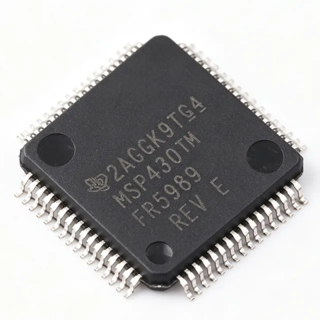
MSP430FR5989IPMR - 128KB FRAM 16MHz Rotary Sensing MCU | TI
MSP430FR5989IPMR

MSP430FR5989IPMR - 128KB FRAM 16MHz Rotary Sensing MCU | TI

The Texas Instruments MSP430FR5989IPMR is a 16-bit ultra-low-power microcontroller based on the MSP430 CPUXV2 RISC core running at up to 16MHz, with 128KB embedded FRAM, 2KB SRAM, and an extended Scan Interface 2 for rotary sensing, housed in a 64-pin LQFP (PM) 10x10mm package. A microcontroller (MCU) is a compact integrated circuit that combines a processor core, program memory, data memory, and programmable peripherals on a single die to govern a specific embedded function. Within the MCU hierarchy, this device belongs to the MSP430 FRAM family of ultra-low-power (ULP) microcontrollers under the broader MSP430 platform and power-management IC taxonomy. Its FRAM (ferroelectric RAM) memory unites SRAM-like speed, flexibility, and endurance with flash-like non-volatility at much lower write energy, eliminating the erase-before-write cycles of conventional flash. Key features include the extended Scan Interface 2 that offloads high-resolution rotary and linear position sensing from the CPU, a hardware AES accelerator for secure metering data, a real-time clock with calendar mode, a 12-bit ADC, comparator, DMA controller, a 32-bit hardware multiplier, and multiple 16-bit timers. Power performance is exceptional: active mode draws approximately 100 uA/MHz and standby (LPM3 with VLO) about 0.4 uA, enabling decade-class battery life in field instruments. Architecturally, the CPUXV2 core executes a 16-bit RISC instruction set over a von Neumann bus at 16MHz. FRAM is byte-writable in-system, allowing fast data logging without external EEPROM, while the AES accelerator encrypts measurements for smart-grid and flow-metering security. The operating supply range is 1.8V to 3.6V with -40C to +85C temperature tolerance for harsh deployments. Typical applications include gas, water, and heat flow meters, rotary and linear position sensing systems, smart-grid endpoints, industrial process control, and secure wireless sensor nodes. Scan Interface 2 directly supports rotary encoders while the CPU sleeps, minimizing average current. Design tip: decouple each VCC pin with 100nF close to the pin plus 10uF bulk capacitance, keep the supply above the SVS threshold for reliable FRAM writes, and use JTAG or two-wire Spy-Bi-Wire for debugging. This page synthesizes distributor pricing, drop-in alternatives, and practical design notes not found in the manufacturer datasheet.

USD $6.30 お問い合わせ