XCKU5P-L2FFVB676E vs XCKU5P-2FFVB676I 比較
詳細な並列比較: XCKU5P-L2FFVB676E メーカー: AMD および XCKU5P-2FFVB676I メーカー: AMD。主要仕様、電気的特性、パッケージ、ライフサイクルステータス、価格、在庫状況を比較して、設計要件に最適な部品を判断してください。

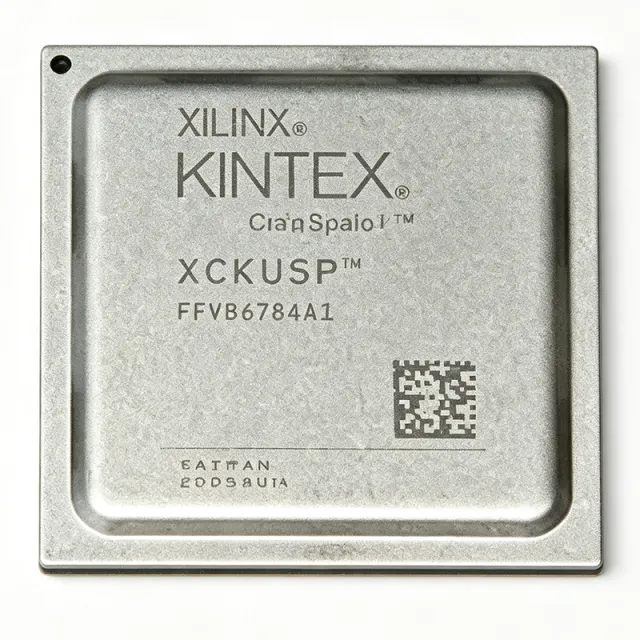
仕様比較
| パラメータ | XCKU5P-L2FFVB676E | XCKU5P-2FFVB676I |
|---|---|---|
| ブランド | AMD | AMD |
| カテゴリ | FPGA & CPLD | FPGA & CPLD |
| ライフサイクル状態 | 有効 | 有効 |
| 単価(USD) | — | $1,660.00 |
| Device Type | Kintex UltraScale+ FPGA | — |
| Logic Blocks | 216,960 blocks | — |
| Macrocells | 474,600 macrocells | — |
| LAB or CLB Count | 27,120 LABs/CLBs | — |
| Total RAM Bits | 41,984,000 bits | — |
| Equivalent RAM Capacity | 16,900 Kbit | — |
| User I/O Count | 280 pins | — |
| パッケージ | 676-pin FCBGA | 676-BBGA, FCBGA (FFVB676) |
| Core Supply Voltage | 0.698 V to 0.876 V | 825 mV to 876 mV |
| Nominal Core Voltage | 0.72 V | — |
| Speed Grade | L2, -2 speed grade | -2 |
| Junction Temperature Range | 0 °C to 110 °C | — |
| Logic Type | Field-programmable gate array | — |
| Device Family | Kintex UltraScale+ | — |
| DSP Compute Performance | 6.3 TeraMACs for the device family | — |
| Backplane Transceiver Classes | 16G and 28G for the device family | — |
| RoHS Compliance | Compliant | — |
| REACH Compliance | Compliant | — |
| DRC Conflict Status | Conflict Free | — |
| 実装タイプ | [DATA_NEEDED: surface-mount mounting classification] | Surface Mount |
| Programmable Flash Capacity | [DATA_NEEDED: configuration flash capacity] | — |
| Transceiver Count | [DATA_NEEDED: exact transceiver count] | — |
| DSP Block Count | [DATA_NEEDED: exact DSP block count] | — |
| Family | — | Kintex UltraScale+ |
| Logic Cells | — | 474600 |
| System Logic Cells | — | 474600 |
| Block RAM | — | 41984000 bits |
| User I/O | — | 280 |
| Maximum Internal Clock Frequency | — | 725 MHz |
| Clock Management | — | MMCM, PLL |
| Process Technology | — | 16 nm FinFET |
| Terminal Form | — | Ball |
| 動作温度 | — | -40C to +100C (Industrial) |
| Temperature Grading | — | Industrial (I) |
| RoHS ステータス | — | Compliant |