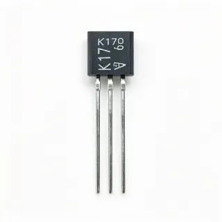
2SK170 - N-Channel Low-Noise Audio JFET, TO-92 | Toshiba
部品番号: 2SK170 ✗ 生産終了| 数量 | 単価 | 小計 |
|---|---|---|
| 1 | $3.5 | $3.50 |
| 10 | $3.15 | $31.50 |
| 100 | $2.8 | $280.00 |
| 500 | $2.45 | $1,225.00 |
| 1,000 | $2.1 | $2,100.00 |
2SK170 概要
A JFET (junction field-effect transistor) is a voltage-controlled semiconductor device in which current flows through a channel whose conductivity is modulated by the gate-source junction, which is reverse-biased. Within the hierarchy of transistor types - transistor -> field-effect transistor -> JFET -> small-signal N-channel JFET - the 2SK170 occupies the low-noise audio niche, offering extremely high input impedance and near-zero gate leakage current that bipolar transistors cannot match.
Key features include ultra-low noise figure optimized for audio-band operation, very high input impedance typical of junction-gate devices, low gate leakage current, and negative gate-source pinch-off voltage suited to simple self-biased common-source and source-follower topologies. The device is supplied in Idss-matched grades - notably GR (2.6 to 6.5 mA) and BL (6 to 12 mA) - allowing designers to select bias current without redesign.
Architecturally, the 2SK170 uses a lateral N-channel silicon junction structure that minimizes 1/f noise, which dominates audio-band noise performance. This is why the part remains the de facto standard for phono preamplifier input stages, microphone head amplifiers, and instrumentation front ends despite its age.
Typical applications include phono cartridge preamps, condenser microphone buffers, hi-fi amplifier input stages, and guitar effects pedals. Its TO-92 package suits hand-assembled audiophile designs and through-hole repair work.
Design consideration: because Idss varies by grade and unit, always source-grade-select or trim source resistors for consistent biasing. Note the device is discontinued by Toshiba; replacement designs should plan for the Linear Systems LSK170.
This page synthesizes distributor sourcing data, drop-in alternatives, and practical design notes not found in the manufacturer datasheet.
ドロップイン代替品: 2SK170 — 同一パッケージでピン互換。PCBの作り直しが必要な異なるパッケージの部品は除外されています。
このシリーズのバリエーション
同一シリーズでドロップイン互換のモデル: 2SK170 (同一形状・フットプリント) — 相違点: Device Type, Mounting Type, Package.
クイック比較ツール — 並列比較する代替部品を選択:
2SK117-GR
✅ ドロップイン ⚠️ 仕様未検証📋 参考代替品(カタログ未掲載)
LSK170A
✅ ドロップイン✓ 在庫あり
$0.94 / 個
データシートを見る →J201
✅ ドロップイン📋 参考代替品(カタログ未掲載)
2SK170 最大定格&電気的特性
| Device Type | N-Channel JFET |
| Drain-Source Voltage (Vdss) | 40 V |
| Drain Current (Id) | 0.02 A |
| パッケージ | TO-92 (3-pin) |
| 実装タイプ | Through Hole |
| Idss Grade GR | 2.6 mA to 6.5 mA |
| Idss Grade BL | 6 mA to 12 mA |
| Application Focus | Low-noise audio amplifier |
| Channel Polarity | N |
| Technology | Silicon N-channel junction type |
| ピン数 | 3 |
| Typical Use Topology | Common-source / source follower |
| Lifecycle | Discontinued (EOL) |
2SK170 ピン構成
| ピン 1 | S — Source |
| ピン 2 | G — Gate |
| ピン 3 | D — Drain |
主な用途
2SK170 の用途: 6 件s: Phono Preamplifier Input Stage, Condenser Microphone Head Amplifier, Hi-Fi Amplifier Input and VAS Stages, Guitar Effects Pedals and Instrument Buffers, Instrumentation and Measurement Front Ends, Active Mixers and VCA-Style JFET Gain Control.
Phono Preamplifier Input Stage
The 2SK170's defining application. Phono cartridges present high source impedance and deliver millivolt-level signals, so the input device's noise dominates the signal-to-noise ratio of the entire playback chain. The 2SK170's ultra-low audio-band noise, near-zero gate leakage, and very high input impedance avoid both cartridge loading and shot-noise contributions. Typical circuits use a GR-grade device (2.6-6.5 mA Idss) in common-source or cascode configuration biased at 2-5 mA. Because the part is discontinued, new phono designs should specify the LSK170, which preserves the same low-noise performance in the same TO-92 footprint.
おすすめ
Condenser Microphone Head Amplifier
Studio condenser microphones use an impedance-converting JFET immediately after the capsule, and the 2SK170 is a classic choice for this position. The capsule needs an essentially infinite-impedance load, which the JFET's reverse-biased gate junction provides, while the device's low noise keeps the self-noise of the microphone below the capsule's thermal noise. Source-follower configurations biased around 1-3 mA from a 48V phantom-derived internal rail are typical. Designers match Idss across channels to keep stereo sensitivity consistent; the BL grade (6-12 mA) suits capsules needing higher drive current.
おすすめ
Hi-Fi Amplifier Input and VAS Stages
High-fidelity power amplifier front ends benefit from the 2SK170 as an input differential pair device or as a voltage-gain stage element. Its low 1/f noise minimizes the amplifier's input-referred noise floor, and its predictable Idss grading (GR/BL) simplifies bias design in long-tailed pairs where matching determines offset and distortion. In source-follower or cascode arrangements biased at several milliamps from regulated rails of 15-40V, the 40V Vdss rating provides adequate headroom. Vintage amplifier restoration frequently replaces failed or counterfeit input JFETs with genuine 2SK170 or the LSK170 equivalent.
おすすめ
Guitar Effects Pedals and Instrument Buffers
DIY guitar effects builders use the 2SK170 in input buffers, boost stages, and JFET-based variable-gain circuits because its high input impedance preserves the tone of high-output-impedance magnetic pickups. Compared with the J201 (Idss roughly 0.2-1 mA), forum measurements note the 2SK170's significantly higher current capability, which yields a stronger buffer with lower output impedance and better drive into tone stacks. A BL-grade device biased around 4-8 mA in source-follower configuration is typical; simple self-bias with one source resistor keeps the circuit to three or four components.
おすすめ
Instrumentation and Measurement Front Ends
Precision measurement instruments such as electrometers, pH amplifiers, and lock-in amplifier front ends need input devices with femtoampere-level gate leakage. The 2SK170's junction-gated structure provides extremely low gate current and low low-frequency noise, letting the amplifier's input noise sit below the transducer's source impedance noise. Circuits typically run the JFET at 1-5 mA drain current with the source degenerated for linearity, often in a matched pair configuration for differential inputs. The discontinued status means new instrument designs should adopt the LSK170, which Linear Systems also supplies in die form for hybrid assemblies.
おすすめ
Active Mixers and VCA-Style JFET Gain Control
JFETs act as voltage-controlled resistors below pinch-off, and the 2SK170 is widely used in audio attenuators, envelope-controlled gain elements, and noise-gate circuits. Its low noise matters because the JFET resistance sits directly in the signal path. Operating with small drain-source voltages (under 100 mV) keeps distortion low, and control voltages of 0 to the pinch-off voltage sweep the channel resistance over a wide range. The GR grade suits low-level signal paths. Designers should temperature-compensate the control loop, since JFET on-resistance drifts with temperature.
おすすめ
おすすめ製品の概要
エンジニアリング参考データ: 2SK170 — 比較、設計ガイダンス、コンプライアンス情報。
選定ガイド
代替品との比較
| パラメータ | この製品 | 2SK117-GR | LSK170 | J201 |
|---|---|---|---|---|
| Package | TO-92 (3-pin) | TO-92 (3-pin) - same | TO-92 (3-pin) - same | TO-92 (3-pin) - same |
| Brand | Toshiba | Toshiba | Linear Systems | onsemi |
| Device Type | N-Channel JFET | N-Channel JFET | N-Channel JFET | N-Channel JFET |
| Idss Range | 2.6-12 mA (grade dependent) | 2.6-6.5 mA (GR) | Graded equivalents of 2SK170 grades | 0.2-1 mA |
| Noise Character | Ultra-low (audio optimized) | Ultra-low (audio optimized) | Ultra-low (audio optimized) | Moderate |
主な差別化要因
- Higher current capability for buffers (vs J201)
- Actively produced direct replacement (vs LSK170)
- Same-family grade flexibility (vs 2SK117-GR)
設計ノート
Do not substitute a Western JFET (e.g. 2N5457 family) without checking pin order - many use D-S-G in TO-92 while the 2SK170 uses the Japanese S-G-D convention. Inserting the wrong part without re-forming leads will forward-bias or short the gate junction. Additionally, always check the Idss grade suffix (GR, BL) on the package: mixing grades in a differential pair produces offset and second-harmonic distortion. Measure Idss yourself (gate shorted to source, 10-15V drain supply) and bin parts before assembly.
Estimated: dissipation is simply Vds x Id. At 15V Vds and 6 mA Idss a 2SK170 dissipates 90 mW, comfortably within TO-92 free-air capability; at 40V Vds and 12 mA (BL grade) it approaches 480 mW, so verify against the datasheet absolute maximum power rating and consider derating at elevated ambient temperature. Keep drain-gate voltage well below the 40V Vdss rating for reliability margin in audio circuits with turn-on transients.
Gate leakage is the enemy of low-noise design: keep the gate node physically away from high-impedance leakage paths, clean flux residue thoroughly after soldering, and consider a guard ring driven at source potential for ultra-high-impedance inputs such as condenser microphone or electrometer front ends. In through-hole TO-92 layouts, minimize the gate trace length to reduce pickup of hum and RF; a small series resistor (1-10 kilo-ohm) at the gate with a shunt capacitance to ground helps RF rejection without audibly loading the source.
コンプライアンス情報
The 2SK170 predates RoHS enforcement; compliance depends on production lot and is not stated in the verified data. The recommended LSK170 replacement is offered in RoHS-compliant versions per Linear Systems.