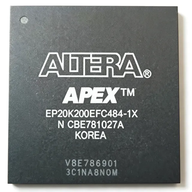
EP20K200EFC484-1X - 200K-Gate APEX 20KE FPGA | 484-FBGA | Intel
部品番号: EP20K200EFC484-1X ✓ 生産中| 数量 | 単価 | 小計 |
|---|---|---|
| 1 | $285 | $285.00 |
| 10 | $245 | $2,450.00 |
| 25 | $215 | $5,375.00 |
| 100 | $185 | $18,500.00 |
| 250 | $165 | $41,250.00 |
EP20K200EFC484-1X 概要
An FPGA is a semiconductor device built around a matrix of configurable logic blocks (CLBs/LABs), programmable interconnect, and I/O cells that can be re-programmed in-system to implement arbitrary digital logic. FPGAs sit between fixed-function ASICs and software-defined processors in the design hierarchy: like an ASIC they implement hardware parallelism at full clock speed, but like a processor they can be re-spin in minutes by changing a bitstream. The APEX 20K family pioneered the MultiCore architecture that combined look-up-table (LUT) logic with embedded dual-port RAM and dedicated carry chains, enabling SOPC (System-On-A-Programmable-Chip) integration in the early 2000s.
The 'E' suffix in APEX 20KE marks the enhanced variant with on-chip PLLs, LVDS I/O support, and a 4× speed-grade bump over the original APEX 20K family. The device integrates 106,496 bits of distributed RAM that can be configured as synchronous dual-port memory, FIFOs, or shift registers - a feature that allowed designers to replace external SRAM in many glue-logic and datapath applications. The 484-FBGA FineLine BGA package (23 × 23 mm) maximizes I/O count for high-pin-count designs while keeping the footprint manageable for four-layer PCB stack-ups.
Typical applications for the EP20K200EFC484-1X include telecommunications line cards, custom datapath accelerators, bus-bridging glue logic, industrial control backplanes, and legacy ASIC prototyping where the design must remain bitstream-portable across Intel/Altera APEX 20K generations. Designers still target this part for long-life-cycle programs in industrial, aerospace, and defense where the APEX 20K bitstream is frozen and certification re-spins are costly.
When designing with this FPGA, pay close attention to the multi-rail power architecture (VCCINT for core, VCCIO banks for I/O, VCC_PLL for PLL, VREF for reference voltages) and use a sequenced power supply to avoid latch-up. Use IBIS models for signal-architecture simulation because the 1.8 V core and LVTTL/LVCMOS I/O standards have very different switching characteristics.
This page synthesizes distributor pricing, drop-in APEX 20K/20KE alternatives in the same 484-FBGA footprint, lifecycle context, and practical design notes not found in any single manufacturer datasheet.
ドロップイン代替品: EP20K200EFC484-1X — 同一パッケージでピン互換。PCBの作り直しが必要な異なるパッケージの部品は除外されています。
このシリーズのバリエーション
同一シリーズでドロップイン互換のモデル: EP20K200EFC484-1X (同一形状・フットプリント) — 相違点: Package, Family, Operating Temperature, Speed Grade, Architecture.
クイック比較ツール — 並列比較する代替部品を選択:
EP20K200EFC484-1
✓ 在庫あり
$68.4 / 個
データシートを見る →EP20K200EFC484-1N
✓ 在庫あり
$290 / 個
データシートを見る →EP20K200EFC484-2X
✓ 在庫あり
$54.4 / 個
データシートを見る →EP20K200EFI484-2X
✓ 在庫あり
$215 / 個
データシートを見る →EP20K200EFC484-1X 最大定格&電気的特性
| Family | APEX 20KE |
| Logic Elements | 8,320 |
| Logic Array Blocks (LABs) | 832 |
| Total RAM Bits | 106,496 |
| Maximum User I/O | 376 |
| Maximum System Gates | 200,000 |
| Process Technology | 0.22 µm CMOS |
| Core Supply Voltage (VCCINT) | 1.71 V to 1.89 V (1.8 V nominal) |
| Propagation Delay | 2.5 ns |
| 動作温度 | 0 °C to +85 °C (Commercial) |
| パッケージ | 484-FBGA (23 × 23 mm, 1.0 mm pitch) |
| 実装タイプ | Surface Mount |
| Architecture | MultiCore (LUT + embedded dual-port RAM) |
| On-chip PLLs | Yes (APEX 20KE enhancement) |
EP20K200EFC484-1X 484-fbga (23 × 23 mm, 1.0 mm pitch) ピン配置ガイド
EP20K200EFC484-1X (484-fbga (23 × 23 mm, 1.0 mm pitch) パッケージ) のピン配置。 このデジタルICには、GPIO、通信インターフェース (UART、SPI、I2C)、および電源ピンが含まれています。代替ピン機能と設定オプションについては、メーカーのデータシートを参照してください。組み込みシステム設計とPCBレイアウトに不可欠です。

詳細なピン配置データはありません: EP20K200EFC484-1X.
詳細は データシート をご参照ください。
主な用途
EP20K200EFC484-1X の用途: 6 件s: Telecommunications Line Card Glue Logic, Custom Datapath Accelerator, Industrial Control Backplane, Legacy ASIC Prototyping, Defense Avionics Display Controller, Test & Measurement Front-End.
Telecommunications Line Card Glue Logic
The EP20K200EFC484-1X's 200K gates, 106 Kbits of embedded dual-port RAM, and 376 user I/O pins make it well suited to telecom line-card glue logic, where the FPGA bridges legacy parallel buses to TDM/E1 framers and protocol controllers. The APEX 20KE MultiCore architecture integrates lookup-table logic with on-chip dual-port RAM blocks, replacing several discrete FIFOs and bus-transceiver CPLDs on a single 23 × 23 mm FBGA. With eight I/O banks supporting mixed LVTTL/LVCMOS/PCI standards, designers can connect 5 V tolerant legacy devices alongside 3.3 V framers on the same die. Compared with modern 7-series FPGAs, the EP20K200EFC484-1X is selected for long-life telecom programs that require bitstream portability and a frozen supply chain across decades of field deployment.
おすすめ
Custom Datapath Accelerator
With 832 LABs and 106,496 embedded RAM bits, the EP20K200EFC484-1X supports custom datapath acceleration tasks such as CRC/checksum engines, packet-parsing pipelines, and Reed-Solomon codecs for storage and networking equipment. The dedicated carry chain in each LAB gives the device sub-2.5 ns adder propagation, while the dual-port RAM blocks enable parallel look-up-table-based packet classification. The -1 commercial speed grade is adequate for 66 MHz PCI and 100 MHz Utopia-style bus interfaces common in 1990s-2000s infrastructure designs. Engineers retrofitting APEX 20KE-based accelerators can drop the EP20K200EFC484-2X for ~20% timing margin when migrating from older APEX 20K (non-E) silicon.
おすすめ
Industrial Control Backplane
Industrial backplanes in PLCs, CNC controllers, and SCADA I/O modules benefit from the EP20K200EFC484-1X's 376 user I/O pins, which can fan out to dozens of optocoupler-isolated 24 V field devices while also providing LVDS links to higher-level controllers. The on-chip PLLs in the APEX 20KE 'E' variant allow multiple clock domains synchronized to a single 50 ppm backplane reference, simplifying board layout compared with external PLL buffers. Industrial programs typically pair this part with the EP20K200EFI484-2X industrial-temperature variant (-40 °C to +100 °C) when the cabinet environment demands extended thermal range. The 484-FBGA FineLine BGA package handles moderate vibration when assembled with underfill and proper corner staking.
おすすめ
Legacy ASIC Prototyping
The EP20K200EFC484-1X serves as a hardware verification platform for legacy ASICs that were originally designed in the early 2000s against the APEX 20KE MultiCore architecture. Engineers porting RTL between silicon revisions can drop new logic into the same 484-FBGA footprint while iterating on micro-architecture, eliminating costly mask set re-spins. The 8,320 logic elements are sufficient for medium-complexity SoC glue logic, memory controllers, and PCI bridge functions. Quartus II's APEX 20KE library provides timing-driven place-and-route with back-annotation support, and the JTAG configuration port allows in-system bitstream updates in minutes. For designs that exceed 200K gates, the EP20K400CB652C7 (400K gates, 652-BGA) provides a denser prototyping target on a Quartus II-compatible flow.
おすすめ
Defense Avionics Display Controller
Defense avionics display controllers rely on the EP20K200EFC484-1X for raster-to-buffer scan conversion, ARINC 429 bus bridging, and MIL-STD-1553 protocol termination because of its long-term availability across multi-decade airframe programs. The commercial 0-85 °C temperature grade is suitable for cockpit electronics with controlled cabin environments, while the EP20K200EFI484-2X industrial variant supports avionics LRUs with extended thermal envelopes. The 1.0 mm FBGA pitch survives high-vibration environments when assembled with corner staking and polymer underfill. APEX 20KE bitstream portability allows DO-254 certification evidence to be reused across hardware revisions, dramatically reducing re-qualification cost on long-life defense programs.
おすすめ
Test & Measurement Front-End
ATE and bench-top test instruments use the EP20K200EFC484-1X to implement custom pattern generation, parallel bus capture, and protocol-aware triggering. The 106,496 bits of dual-port RAM serve as deep FIFO storage for captured waveforms, while the 376 I/Os can fan out to dozens of instrument channels in parallel. LVDS-capable I/O banks allow direct connection to high-speed ADC/DAC front-ends without external buffers. Engineers value the part for its deterministic timing and the maturity of the Quartus II toolchain, which remains in use at many test-equipment OEMs because bit-for-bit compatibility with deployed test programs is mandatory. The 484-FBGA footprint also supports controlled-impedance signal routing for sub-ns edge rates required by modern gigasample ADCs.
おすすめ
おすすめ製品の概要
エンジニアリング参考データ: EP20K200EFC484-1X — 比較、設計ガイダンス、コンプライアンス情報。
選定ガイド
代替品との比較
| パラメータ | この製品 | EP20K200EFC484-1 | EP20K200EFC484-1N | EP20K200EFC484-2X | EP20K200EFI484-2X |
|---|---|---|---|---|---|
| Package | 484-FBGA (23 × 23 mm) | 484-FBGA (23 × 23 mm) - same | 484-FBGA (23 × 23 mm) - same | 484-FBGA (23 × 23 mm) - same | 484-FBGA (23 × 23 mm) - same |
| Brand | Intel (Altera) | Intel (Altera) | Intel (Altera) | Intel (Altera) | Intel (Altera) |
| Speed Grade | -1 (slower) | -1 (same) | -1 (same) | -2 (faster, ~20%) | -2 (faster, ~20%) |
| Operating Temperature | 0 to 85 °C (Commercial) | 0 to 85 °C (Commercial) | 0 to 85 °C (Commercial) | 0 to 85 °C (Commercial) | -40 to 100 °C (Industrial) |
| Ball Finish | Lead-free (SnAgCu) | Lead-bearing (SnPb) | Lead-free (SnAgCu) | Lead-free (SnAgCu) | Lead-free (SnAgCu) |
| System Gates | 200,000 | 200,000 | 200,000 | 200,000 | 200,000 |
| Logic Elements | 8,320 | 8,320 | 8,320 | 8,320 | 8,320 |
| Embedded RAM Bits | 106,496 | 106,496 | 106,496 | 106,496 | 106,496 |
| User I/O Pins | 376 | 376 | 376 | 376 | 376 |
| Lifecycle Status | Obsolete | Obsolete | Obsolete | Obsolete | Obsolete |
主な差別化要因
- Lead-free RoHS-compliant ball finish with identical silicon to legacy variants (vs EP20K200EFC484-1)
- Faster -2 speed grade available in identical 484-FBGA footprint (vs EP20K200EFC484-1X)
- Industrial temperature range option for harsh-environment drop-in (vs EP20K200EFC484-2X)
- 200K-gate APEX 20KE density with MultiCore LUT+RAM architecture (vs EP20K100FC324-1 (smaller APEX 20K))
設計ノート
The APEX 20KE requires three independent supplies: VCCINT (1.71-1.89 V, ~1 A full-load), VCCIO per bank (1.8 V / 2.5 V / 3.3 V depending on I/O standard, ~0.5 A peak per bank), and VCC_PLL (1.8 V analog, low-noise). Use a sequenced power controller such as the LTC2955 to ramp VCCINT before VCCIO to avoid CMOS latch-up; the EP20K200EFC484-1X core can draw 200 mA in-rush during configuration. Decouple every VCCINT pin with a 0.1 µF X7R ceramic plus a 10 µF bulk tantalum placed within 5 mm of the BGA footprint.
The 484-FBGA uses a 1.0 mm ball pitch and 23 × 23 mm body, requiring a 6-layer PCB stack-up with 0.5 oz copper and a low-CTE (Tg ≥ 150 °C) substrate. Use 0.5 mm NSMD pads with 0.6 mm solder-mask openings, and route signal escape on the top layer only via micro-vias (0.1 mm). For controlled-impedance LVDS pairs, target 100 Ω differential with 0.2 mm-wide traces, length-matched within 0.5 mm. Apply corner staking or underfill (Loctite 3563) to improve thermal-cycle reliability in vibration-prone enclosures.
On-chip PLLs in the APEX 20KE require a quiet 1.8 V VCC_PLL supply - place an LC pi-filter (ferrite bead + 10 µF + 0.1 µF) within 5 mm of the PLL power pin and isolate the PLL ground from the digital ground with a split plane that joins only at the PCB ground star. Reference clock lines to the PLL should be routed over a continuous ground plane and length-matched to within 2 mm. For LVDS outputs above 200 Mbps, source-terminate (100 Ω across the LVDS pair) at the FPGA end and verify eye opening with an IBIS model simulation in Quartus II SignalTap.
Do not mix 5V signals on I/O banks powered at 3.3 V or lower - APEX 20KE I/O tolerance is strictly VCCIO + 0.3 V, and 5V inputs will forward-bias the I/O ESD diodes. When migrating from APEX 20K (non-E) to APEX 20KE, recompile with the Quartus II 4.2 or later library because the E variant adds LVDS I/O and PLL primitives that do not exist in the original APEX 20K architecture. Finally, do not program the device with a Quartus Prime bitstream - the toolchain recognizes only Quartus II 4.x through 13.0sp1 SOF/POF files for APEX 20KE.
コンプライアンス情報
The '-X' suffix denotes lead-free (SnAgCu) ball finish, which is RoHS-compliant per Altera/Intel PCN documentation. REACH, halogen-free, and conflict-minerals compliance were not specified in the verified web data and are marked unknown. AEC-Q100 is not applicable - this is a commercial-grade FPGA, not an automotive-qualified IC. Industrial-temperature (-40 to +100 C) operation requires the EP20K200EFI484-2X variant.







